1. WORKSHEET – How PV Solar Works
How Solar Cells Turn Sunlight into Electricity
Solar cells are materials that turn sunlight into electricity. This effect was first recorded by E.
Becquerel, in 1839. The first solid state device was recorded to show such an effect in 1877.
However, it was in 1954 at Bell Labs when the solar electric effect was demonstrated in silicon
(Si) that the idea of producing useable amounts of electricity from solar cells began.
The question is, how do solar cells produce electricity?
Two facts are important to the understanding of how solar cells work.
• First, sunlight is composed of photons of various energies.
• Second, photons can interact with atoms, and if a photon has sufficient energy, it can break
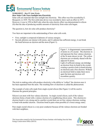
the bond between an electron and the atom (Figure 1).
Figure 1. A diagrammatic representation
of atoms in a Si crystal. The electrons in
red represent the four valence electrons
of the Si atom shown in red. The yellow
electrons are covalently shared with the
adjacent Si atoms.
Light of sufficient energy can dislodge
an electron from its bond in the crystal,
creating a positive hole (a bond missing
an electron) and a free electron. Without
an electrical field to make them move
apart the hole and electron will
recombine quickly.
The trick to making solar cells produce electricity is the ability to “collect” the electron once it
has been separated from the atom. The resulting flow of electrons is called the photocurrent.
The example of solar cells made from single crystal silicon (like Figure 1) will be used to
illustrate the general principles.
Silicon is an atom with four valence electrons. In single crystal silicon, each of the valence
electrons forms a bond with a valence electron of a neighboring silicon atom. This electron-to-
electron bond is very strong and in a perfect crystal there are no free valence electrons waiting
to bond with another electron. Electrons bond in pairs when possible (it’s lower energy state).
Pure single crystal silicon is a very poor conductor because all the valence electrons are bonded
with their neighbors.
This lesson plan created by the Environmental Science Institute with funding from the State
Energy Conservation Office (SECO)
2. To collect the photocurrent, solar cells are constructed like a battery. This is done by taking two
semiconductors of opposite charge and putting them together (Figure 2).
To make Figure 2. A diagrammatic
solar cell representation of a simple solar
cell. When n- (doped with P)
and p-type (doped with B)
silicon come into contact,
electrons move from the n-side
to the p-side. This causes a
positive charge to build on the
n-side of the interface (or p-n
junction) and a negative charge
to form on the p-side.
semiconductor material
from silicon approximately 2x10¹⁶/cm3 acceptor atoms (atoms with three valence electrons such
as boron, B) or approximately 1019/cm3 donor atoms (atoms with five valence electrons such as
phosphorous, P) are substituted for the silicon atoms with four valence electrons.
When phosphorous is substituted for a silicon atom, four of the five valence electrons form
strong bonds with the nearest silicon electrons and the remaining electron is very loosely bound
by the slightly more positive charge of the nucleus of the phosphorous atom. However, this
electron travels easily around the crystal lattice in the area of the phosphorous atom. Silicon
that contains atoms with an extra valence electron is called n-type silicon (n is for negative).
The process of substituting boron or phosphorous atoms for silicon atoms is called doping.
This is often done by thermal diffusion.
If a boron atom is substituted for a silicon atom, the three valence electrons form strong bonds
with the nearest silicon electrons, but there is one silicon electron that is left looking for a
partner to bond with. This missing electron that is being sought for bonding, is called a hole.
Because the hole is a missing electron, it can be treated mathematically like the free electron
when phosphorous is substituted, but it effectively has a positive charge (the absence of an
negative electron). Silicon that contains atoms with one less valence electron is called p-type
silicon (p is for positive).
A solar battery is created when n and p type silicon are placed next to each other. The extra
electrons from the phosphorous are attracted to the holes created by the doping of the silicon
with boron (Figure3). This occurs because binding of the electron pairs is much stronger than
the electromagnetic attraction between the outer electrons and the nucleus of the atoms that is
masked by the electrons that are surrounding each atom in the crystal structure.
Near the junction of the n and p type material, holes on the p-side are filled with the free
electrons from the n-side forming strong, stable electron pair bonds (Figure 3). This results in a
shift in charge that creates an electric field in the material. When the free valence electron from
the n-side combines with the single bound valence electron on the p-side, the phosphorus atom
This lesson plan created by the Environmental Science Institute with funding from the State
Energy Conservation Office (SECO)
3. is surrounded by one less electron than there are positive protons in the phosphorus nucleus.
Similarly, the boron atom is surrounded by one more electron than there are positive protons in
the boron nucleus. While this n-p ‘junction’ is only a few atoms thick, the resulting electric
field creates a barrier that prevents additional crossover of holes from the p-side and electrons
from the n-side. This electric field (resulting in an electromotive force, EMF, of approximately
0.5 volts) makes it possible to create the photocurrent when light breaks the electron-electron
pair bond. All that is need now is light energy to make electricity.
n-Side p-Side Figure 3. The buildup of excess
_ positive and negative charges
Phosphorous + Boron on either side of the junction
_ creates an electric field across
_ +
_ the interface; the strength of this
Junction
+ field depends on the amount of
_ dopant in the silicon. At
+ equilibrium, the electric field
_
+ +
repels any additional crossover
of holes from the p-side or
electrons from the n-side.
Now, when the photon enters the material and breaks apart an electron pair (Figure 4), a
negative electron and a positive hole are created. If it weren’t for the electric field, the electron
and the hole would attract and recombine. With the electric field, the negative electron goes
one direction and the positive hole goes the other direction. The electric field acts as a diode,
allowing electrons to flow only from the p side to the n side, but not the other way. This is the
source of the electricity of a solar cell. The movement of electrons in one direction (and positive
holes in the other) is the definition of electrical current. Solar cells have grids of conductive
wire near the surface (not shown in the diagrams) to lead this current to the electrical system to
be powered or to charge batteries.
n-Side p-Side Figure 4. When sunlight
striking a cell creates
Phosphorous Boron charge carriers (electrons
+
_ and holes), the electric
field pushes new electrons
Junction
to one side of the junction
+ and new holes to the
other. This sorting-out
process is what drives the
_ charge carriers in an
electric circuit.
This lesson plan created by the Environmental Science Institute with funding from the State
Energy Conservation Office (SECO)
4. The minimum energy that it takes to break up the electron-electron bond is called the band gap.
Photons with energy less than the band gap won’t separate the electron pairs. Photons with
more energy than necessary to separate the electron pairs result in electrons and holes with more
kinetic energy. The term band gap refers to the energy necessary to separate the electron pair. It
can also be thought of as the energy necessary to make an electron in the valence band jump
into the conduction band. The valence band is where the electrons are bonded and the
conduction band is where the electrons are free to flow as a current. When the electron pairs are
separated by a photon, any energy of the photon above the band gap energy goes into the kinetic
energy of the electron.
When solar cells get hot, the electrons and atoms are vibrating faster and the effectiveness of the
electric field to separate the electrons and holes is diminished. The randomly directed kinetic
energy becomes the dominant factor governing the motion of the electrons and holes. Typical
loss in efficiency is about 0.1%/degree C measured solar cell temperature. (A solar cell that is
16% efficient at 25º C will be 9% efficient at 100º C)
[Figures based on slides from the National Renewable Energy Laboratory]
Questions for group or individual consideration:
1) What atomic property makes Si a useful material for making solar cells? Is there
another element that might be used for the same reasons?
2) Similarly, what atomic properties of B and P are exploited when they are added in small
amounts to Si photovoltaic cell materials?
3) What is p-type Si ? n-type? What do the p and n stand for?
4) What is a “hole” in a Si crystal?
5) Describe the movement of electrons and holes when p-type and n-type Si are joined
together. Do all the electrons and holes travel across the p-n junction to balance charges?
Why or why not?
6) What happens when energetic light photons interact with the Si in a p and n type solar
cell? What “sorts out” or drives the electrons away from the holes so they don’t re-
combine?
7) Is the current from a solar cell AC or DC?
8) Let’s consider some real-world data. Go to the website
http://www.soltrex.com/index.cfm. Get you teacher’s permission first (she may have
already registered) then register to use the system (bottom of the orange box on the
right). When you have logged in, click on EXPLORE SYSTEMS on the upper black
banner. Type in Bryker to get to the solar data being collected by Bryker Woods
Elementary School’s solar power system. On the page that comes up click on the blue
Bryker Woods link. A graph of power output will be displayed for the PV system. You
can roll over the other types of graphs to get an idea of what current conditions are like.
Next, click on the “Custom” button to the right of the graph. In the Graph Controls
orange box on the right enter the date range 01/01/2008 to 12/31/2008 (or any year
period you like), set the Interval to “Day” and the Data Set to “Energy Production
(kWh)”.
a. What times of the year have the highest daily energy outputs?
b. What times of the year have the most day-to-day-variability? Why?
This lesson plan created by the Environmental Science Institute with funding from the State
Energy Conservation Office (SECO)
5. c. It was noted above that solar cells become less efficient as temperature rises. Is
the summer to winter temperature difference (approximately 30°C) enough to
account for the monthly difference in energy production?
d. Consider where the sun is in the sky in summer versus winter. How would you
align and tilt a solar panel to get the most power over the whole year? This is not
a simple question! Change the Interval on the graph to month or quarter and
you’ll see that this solar power system has been set up to even out much of the
variation in power production over a year, but to get a little more in the summer.
When in the year do you think energy demand is highest in Austin Texas?
Further resources and follow up: There are numerous websites with information on this topic.
The University of Oregon's Solar Radiation Monitoring Lab maintains a site at
http://solardat.uoregon.edu/ that has solar data, information about solar monitoring, and lists and
links to many other sites. A nice supplement to the teaching
Useful Web Sites:
http://science.howstuffworks.com/solar-cell.htm
http://www.soltrex.com/index.cfm.
http://www.nrel.gov/ncpv/
http://www.ascensiontech.com/RTD/ashlandrtd.html
http://www.ascensiontech.com/RTD/pge.html
http://www.ases.org/
http://www.seia.org/main.htm
http://www.pvwatts.org/
For further reading:
The Solar Electric House by Steven J. Strong with William G. Scheller, Sustainability Press,
Still River, Massachusetts 01467-0143, 1987.
From Space to Earth – The Story of Solar Electricity, John Perlin, aatec publications, Ann
Arbor, MI 48107, 1999.
The Solar Electricity Handbook 2009: A Simple, Practical Guide to Using Electric Solar Panels
and Designing and Installing Photovoltaic Solar PV Systems by Michael Boxwell: CodeGreen
Publishing, Ryton on Dunsmore, UK,.
This lesson plan created by the Environmental Science Institute with funding from the State
Energy Conservation Office (SECO)