SlideShare a Scribd company logo
1 of 65
Now we have understood,
 For any signal to be considered as logic ‘0’ and logic ‘1’, it should be in the NML and
 NMH ranges, respectively


3/2/2013                                                                                   1
Now we have understood,
 For any signal to be considered as logic ‘0’ and logic ‘1’, it should be in the
 NML and NMH ranges, respectively


  Now, let us understand the factors affecting the voltage levels to vary from this range
3/2/2013                                                                              2
Ideal
                                                                       Switching
                                                                        Activity


                                                                              Actual
                                                                             Switching
                                                                              Activity


Switching Activity of a Device is one of the factors which affects the voltage levels of
Input/Output signals
Vdd


                          Poly Gate
                                             PMOS – P Diff

                     In                            Out

                                              NMOS – N Diff


                                          Vss


Lets understand the internal process while Switching Activity happens in a Device
Vdd


                         Poly Gate
                                            PMOS – P Diff

                    In                           Out

                                            NMOS – N Diff


                                         Vss


               PMOS                                          NMOS
Consider the MOS device, to understand the actual scenario
PMOS                                         NMOS


   Let’s revise MOS device characteristics
MOS device characteristics


                                                             G

                                                     Vgs


                                                 S                D
                                                           NMOS


                    Vgs is the Voltage between gate and source
MOS device characteristics


            G

    Vgs


S                     D
          NMOS
MOS device characteristics


            G

    Vgs
                                    Vgs < VT (Threshold Voltage)
                                                                   S                  D

S                     D
          NMOS


                      If Vgs   is   less then VT , the NMOS will act as Open Switch
MOS device characteristics


            G

    Vgs
                                    Vgs > VT (Threshold Voltage)
                                                                   S                   D

S                     D
          NMOS


                      If Vgs   is   greater then VT , the NMOS will act as Closed Switch
MOS device characteristics


            G

    Vgs                              Vgs > VT

                                 S              D

S                     D
          NMOS
MOS device characteristics


               G

    Vgs                                                                 Vgs > VT

                                               S                                   D

S                        D
             NMOS

          When MOSFET is ‘ON’, it can be modeled as a ‘Resistor’ with switch closed

          When MOSFET is ‘OFF’, it can be modeled as an ‘open switch’
When MOSFET is ‘ON’, it can be modeled as a ‘Resistor’ with closed switch
When MOSFET is ‘ON’, it can be modeled as a ‘Resistor’ with switch closed


PMOS acts as Logic ‘0’                        NMOS acts as Logic ‘1’
When MOSFET is ‘ON’, it can be modeled as a ‘Resistor’ with switch closed


PMOS acts as Logic ‘0’                        NMOS acts as Logic ‘1’
When MOSFET is ‘OFF’, it can be modeled as an ‘open switch’
When MOSFET is ‘ON’, it can be modeled as a ‘Resistor’ with switch closed


 PMOS acts as Logic ‘0’                        NMOS acts as Logic ‘1’
 When MOSFET is ‘OFF’, it can be modeled as an ‘open switch’


       PMOS                                          NMOS

PMOS acts as Logic ‘1’                        NMOS acts as Logic ‘0’
Vdd


In                      Out


               Vss


     Input Switching from logic ‘1’ to logic ‘0’
Vdd


In                      Out


               Vss


     Input Switching from logic ‘1’ to logic ‘0’

     NMOS is turning ‘OFF’
Vdd


In                      Out


               Vss


     Input Switching from logic ‘1’ to logic ‘0’

     NMOS is turning ‘OFF’

     PMOS is turning ‘ON’
Input Switching from logic ‘1’ to logic ‘0’

NMOS is turning ‘OFF’
Input Switching from logic ‘1’ to logic ‘0’

NMOS is turning ‘OFF’

PMOS is turning ‘ON’
Input Switching from logic ‘1’ to logic ‘0’

            NMOS is turning ‘OFF’

            PMOS is turning ‘ON’


     Vdd


In         Out


     Vss
Input Switching from logic ‘1’ to logic ‘0’

                              NMOS is turning ‘OFF’

                              PMOS is turning ‘ON’


                    Vdd                                   Vdd


                                                      R

In                          Out                                   Out


                    Vss                                   Vss


     Replace PMOS as resistor and NMOS by open switch.
Input Switching from logic ‘1’ to logic ‘0’

                         NMOS is turning ‘OFF’

                         PMOS is turning ‘ON’


                 Vdd                                   Vdd


             R                                     R

                       Out                                             Out

                                                                 CL


                 Vss                                   Vss


Connect Capacitor on output end.
Input Switching from logic ‘1’ to logic ‘0’

                             NMOS is turning ‘OFF’

                             PMOS is turning ‘ON’


              Vdd


          R

                             Out

                        CL


              Vss


Consider Capacitor is charged when Vdd is applied.
Input Switching from logic ‘1’ to logic ‘0’

                            NMOS is turning ‘OFF’

                            PMOS is turning ‘ON’


              Vdd


          R

                            Out

                       CL


              Vss


Consider Capacitor is charged up to Vdd
Input Switching from logic ‘1’ to logic ‘0’

               NMOS is turning ‘OFF’

               PMOS is turning ‘ON’


    Vdd


R

               Out

          CL


    Vss
Summary


     Vdd                 Vdd


                     R

In         Out                      Out

                               CL


     Vss                 Vss
Summary


                                                    Vdd


                                                R

                                                                   Out

                                                              CL


                                                    Vss


Lets convert the area within dotted lines into closed loop circuit.
Summary


                                                   Vdd


       R                                       R

                                                              Out
Vdd                   CL
                                                         CL


                                                   Vss


      Lets convert into closed loop circuit.
Summary


                         Capacitor Models


      R


Vdd       CL
Summary


                                  Capacitor Models


      R            Uncharged Cap           +
                                             0V             short
                                           -

Vdd       CL
                                           +                +
                    Charged Cap              V                VO
                                           - O              -


                                           +
                  Fully Charged Cap          Open circuit
                                           -
Summary


                         Waveforms


      R


Vdd       CL
Summary


                               Waveforms


                         Vdd

      R


Vdd       CL
Summary


                               Waveforms


                         Vdd

      R

                         VCL
Vdd       CL
Summary


                               Waveforms


                         Vdd

      R

                         VCL
Vdd       CL

                         VR
Summary


                               Waveforms


                         Vdd

      R

                         VCL
Vdd       CL

                         VR


                                  I = V/R
Summary


                               Waveforms


                         Vdd

      R

                         VCL
Vdd       CL

                         VR


                                  I = V/R

                         IR
Summary


                                 Waveforms


                           Vdd

      R

                           VCL
Vdd       CL

                           VR


                                    I = V/R
                   Ipeak
                           IR
So what can we conclude!!!


A capacitor needs at least Ipeak amount of current
So what can we conclude!!!


A capacitor needs at least Ipeak amount of current


Ipeak
        IR
So what can we conclude!!!


A capacitor needs at least Ipeak amount of current


Ipeak
        IR


               To get charged upto Vdd voltage
So what can we conclude!!!


A capacitor needs at least Ipeak amount of current


Ipeak
        IR


               To get charged upto Vdd voltage


             VCL
So what can we conclude!!!


A capacitor needs at least Ipeak amount of current


Ipeak
        IR


               To get charged upto Vdd voltage


             VCL


And, the output of inverter, is recognized as logic ‘1’
So what can we conclude!!!


A capacitor needs at least Ipeak amount of current


Ipeak
        IR


               To get charged upto Vdd voltage


             VCL


And, the output of inverter, is recognized as logic ‘1’
And, the output of inverter, is recognised as logic ‘1’


             What does this mean????
And, the output of inverter, is recognised as logic ‘1’


                   What does this mean????


     It means that the voltage across capacitor

     Vpeak
             VCL
And, the output of inverter, is recognised as logic ‘1’


                   What does this mean????


     It means that the voltage across capacitor

     Vpeak
             VCL


        Lies in NMH level of noise margin graph
Vdd
VOH
            NMH
VIH         Noise Margin High


                                NMH = VOH - VIH

                                NML = VIL - VOL

VIL         NML
            Noise Margin High
VOL

      0
Why to do?


3/2/2013                65

More Related Content

What's hot (20)

Low power vlsi design
Low power vlsi designLow power vlsi design
Low power vlsi design
 
Vlsi design and fabrication ppt
Vlsi design and fabrication  pptVlsi design and fabrication  ppt
Vlsi design and fabrication ppt
 
Michael john sebastian smith application-specific integrated circuits-addison...
Michael john sebastian smith application-specific integrated circuits-addison...Michael john sebastian smith application-specific integrated circuits-addison...
Michael john sebastian smith application-specific integrated circuits-addison...
 
CMOS LOGIC STRUCTURES
CMOS LOGIC STRUCTURESCMOS LOGIC STRUCTURES
CMOS LOGIC STRUCTURES
 
Rc delay modelling in vlsi
Rc delay modelling in vlsiRc delay modelling in vlsi
Rc delay modelling in vlsi
 
BGR
BGRBGR
BGR
 
Physical Verification Design.pdf
Physical Verification Design.pdfPhysical Verification Design.pdf
Physical Verification Design.pdf
 
Cmos fabrication
Cmos fabricationCmos fabrication
Cmos fabrication
 
Synchronous and asynchronous clock
Synchronous and asynchronous clockSynchronous and asynchronous clock
Synchronous and asynchronous clock
 
Low Power VLSI Design
Low Power VLSI DesignLow Power VLSI Design
Low Power VLSI Design
 
Design and development of carry select adder
Design and development of carry select adderDesign and development of carry select adder
Design and development of carry select adder
 
Actel fpga
Actel fpgaActel fpga
Actel fpga
 
minimisation of crosstalk in VLSI routing
minimisation of crosstalk in VLSI routingminimisation of crosstalk in VLSI routing
minimisation of crosstalk in VLSI routing
 
MULTI Threshold
MULTI ThresholdMULTI Threshold
MULTI Threshold
 
Study of vlsi design methodologies and limitations using cad tools for cmos t...
Study of vlsi design methodologies and limitations using cad tools for cmos t...Study of vlsi design methodologies and limitations using cad tools for cmos t...
Study of vlsi design methodologies and limitations using cad tools for cmos t...
 
CMOS TG
CMOS TGCMOS TG
CMOS TG
 
Cmos logic
Cmos logicCmos logic
Cmos logic
 
Vlsi testing
Vlsi testingVlsi testing
Vlsi testing
 
Mos transistor
Mos transistorMos transistor
Mos transistor
 
Ppt career
Ppt careerPpt career
Ppt career
 

Viewers also liked

Floorplan (http://www.vlsisystemdesign.com/PD-Flow.php)
Floorplan (http://www.vlsisystemdesign.com/PD-Flow.php)Floorplan (http://www.vlsisystemdesign.com/PD-Flow.php)
Floorplan (http://www.vlsisystemdesign.com/PD-Flow.php)VLSI SYSTEM Design
 
Define location of Preplaced cells(http://www.vlsisystemdesign.com/PD-Flow.php)
Define location of Preplaced cells(http://www.vlsisystemdesign.com/PD-Flow.php)Define location of Preplaced cells(http://www.vlsisystemdesign.com/PD-Flow.php)
Define location of Preplaced cells(http://www.vlsisystemdesign.com/PD-Flow.php)VLSI SYSTEM Design
 
Define Width and Height of Core and Die (http://www.vlsisystemdesign.com/PD-F...
Define Width and Height of Core and Die (http://www.vlsisystemdesign.com/PD-F...Define Width and Height of Core and Die (http://www.vlsisystemdesign.com/PD-F...
Define Width and Height of Core and Die (http://www.vlsisystemdesign.com/PD-F...VLSI SYSTEM Design
 
Time saver project template
Time saver project templateTime saver project template
Time saver project templateKim Cao
 
E sky2u.com marketing plan v3.0
E sky2u.com marketing plan v3.0E sky2u.com marketing plan v3.0
E sky2u.com marketing plan v3.0e-sky, Inc
 
BÍ QUYẾT QUẢN LÝ HIỆU QUẢ CÂU LẠC BỘ CHA MẸ VÀ VỊ THÀNH NIÊN, THANH NIÊN
BÍ QUYẾT QUẢN LÝ HIỆU QUẢ CÂU LẠC BỘ CHA MẸ VÀ VỊ THÀNH NIÊN, THANH NIÊNBÍ QUYẾT QUẢN LÝ HIỆU QUẢ CÂU LẠC BỘ CHA MẸ VÀ VỊ THÀNH NIÊN, THANH NIÊN
BÍ QUYẾT QUẢN LÝ HIỆU QUẢ CÂU LẠC BỘ CHA MẸ VÀ VỊ THÀNH NIÊN, THANH NIÊNCGFED
 
Financial aid assistance
Financial aid assistanceFinancial aid assistance
Financial aid assistancelupitacm
 
CCP's Mishu System Tsai and Dean
CCP's Mishu System Tsai and DeanCCP's Mishu System Tsai and Dean
CCP's Mishu System Tsai and DeanSAINBAYAR Beejin
 
Comment Letter on New Regulations Addressing BDPOs -- Letter dated January 3,...
Comment Letter on New Regulations Addressing BDPOs -- Letter dated January 3,...Comment Letter on New Regulations Addressing BDPOs -- Letter dated January 3,...
Comment Letter on New Regulations Addressing BDPOs -- Letter dated January 3,...Samuel Grilli
 
Show me your hands
Show me your handsShow me your hands
Show me your handsTerry Penney
 
Case study: #GoogleMoLang
Case study: #GoogleMoLangCase study: #GoogleMoLang
Case study: #GoogleMoLangnoreensayoc
 
International trade course 3
International trade course 3International trade course 3
International trade course 3Yudy Yunardy
 

Viewers also liked (20)

Floorplan (http://www.vlsisystemdesign.com/PD-Flow.php)
Floorplan (http://www.vlsisystemdesign.com/PD-Flow.php)Floorplan (http://www.vlsisystemdesign.com/PD-Flow.php)
Floorplan (http://www.vlsisystemdesign.com/PD-Flow.php)
 
Place decap
Place decapPlace decap
Place decap
 
Need of Decoupling Capacitor
Need of Decoupling CapacitorNeed of Decoupling Capacitor
Need of Decoupling Capacitor
 
Define location of Preplaced cells(http://www.vlsisystemdesign.com/PD-Flow.php)
Define location of Preplaced cells(http://www.vlsisystemdesign.com/PD-Flow.php)Define location of Preplaced cells(http://www.vlsisystemdesign.com/PD-Flow.php)
Define location of Preplaced cells(http://www.vlsisystemdesign.com/PD-Flow.php)
 
Define Width and Height of Core and Die (http://www.vlsisystemdesign.com/PD-F...
Define Width and Height of Core and Die (http://www.vlsisystemdesign.com/PD-F...Define Width and Height of Core and Die (http://www.vlsisystemdesign.com/PD-F...
Define Width and Height of Core and Die (http://www.vlsisystemdesign.com/PD-F...
 
Time saver project template
Time saver project templateTime saver project template
Time saver project template
 
E sky2u.com marketing plan v3.0
E sky2u.com marketing plan v3.0E sky2u.com marketing plan v3.0
E sky2u.com marketing plan v3.0
 
BÍ QUYẾT QUẢN LÝ HIỆU QUẢ CÂU LẠC BỘ CHA MẸ VÀ VỊ THÀNH NIÊN, THANH NIÊN
BÍ QUYẾT QUẢN LÝ HIỆU QUẢ CÂU LẠC BỘ CHA MẸ VÀ VỊ THÀNH NIÊN, THANH NIÊNBÍ QUYẾT QUẢN LÝ HIỆU QUẢ CÂU LẠC BỘ CHA MẸ VÀ VỊ THÀNH NIÊN, THANH NIÊN
BÍ QUYẾT QUẢN LÝ HIỆU QUẢ CÂU LẠC BỘ CHA MẸ VÀ VỊ THÀNH NIÊN, THANH NIÊN
 
Financial aid assistance
Financial aid assistanceFinancial aid assistance
Financial aid assistance
 
Historia del computador
Historia del computadorHistoria del computador
Historia del computador
 
Transformator
TransformatorTransformator
Transformator
 
CCP's Mishu System Tsai and Dean
CCP's Mishu System Tsai and DeanCCP's Mishu System Tsai and Dean
CCP's Mishu System Tsai and Dean
 
How To Promote Your Business On Pinterest
How To Promote Your Business On PinterestHow To Promote Your Business On Pinterest
How To Promote Your Business On Pinterest
 
Primary EFL Reading Competition
Primary EFL Reading CompetitionPrimary EFL Reading Competition
Primary EFL Reading Competition
 
Comment Letter on New Regulations Addressing BDPOs -- Letter dated January 3,...
Comment Letter on New Regulations Addressing BDPOs -- Letter dated January 3,...Comment Letter on New Regulations Addressing BDPOs -- Letter dated January 3,...
Comment Letter on New Regulations Addressing BDPOs -- Letter dated January 3,...
 
NASA RFP
NASA RFPNASA RFP
NASA RFP
 
Show me your hands
Show me your handsShow me your hands
Show me your hands
 
Opjo
OpjoOpjo
Opjo
 
Case study: #GoogleMoLang
Case study: #GoogleMoLangCase study: #GoogleMoLang
Case study: #GoogleMoLang
 
International trade course 3
International trade course 3International trade course 3
International trade course 3
 

Similar to Switching activity

MOS as Diode, Switch and Active Resistor
MOS as Diode, Switch and Active ResistorMOS as Diode, Switch and Active Resistor
MOS as Diode, Switch and Active ResistorSudhanshu Janwadkar
 
Digital ic ajal crc
Digital ic ajal crcDigital ic ajal crc
Digital ic ajal crcAJAL A J
 
Power mosfet characteristics
Power mosfet characteristicsPower mosfet characteristics
Power mosfet characteristicssanu singh
 
CMOS Topic 5 -_cmos_inverter
CMOS Topic 5 -_cmos_inverterCMOS Topic 5 -_cmos_inverter
CMOS Topic 5 -_cmos_inverterIkhwan_Fakrudin
 

Similar to Switching activity (7)

MOS as Diode, Switch and Active Resistor
MOS as Diode, Switch and Active ResistorMOS as Diode, Switch and Active Resistor
MOS as Diode, Switch and Active Resistor
 
Transistor
TransistorTransistor
Transistor
 
IC_Lectures_Updated.pdf
IC_Lectures_Updated.pdfIC_Lectures_Updated.pdf
IC_Lectures_Updated.pdf
 
Digital ic ajal crc
Digital ic ajal crcDigital ic ajal crc
Digital ic ajal crc
 
Power mosfet characteristics
Power mosfet characteristicsPower mosfet characteristics
Power mosfet characteristics
 
Low Power Techniques
Low Power TechniquesLow Power Techniques
Low Power Techniques
 
CMOS Topic 5 -_cmos_inverter
CMOS Topic 5 -_cmos_inverterCMOS Topic 5 -_cmos_inverter
CMOS Topic 5 -_cmos_inverter
 

Recently uploaded

How to Manage Global Discount in Odoo 17 POS
How to Manage Global Discount in Odoo 17 POSHow to Manage Global Discount in Odoo 17 POS
How to Manage Global Discount in Odoo 17 POSCeline George
 
This PowerPoint helps students to consider the concept of infinity.
This PowerPoint helps students to consider the concept of infinity.This PowerPoint helps students to consider the concept of infinity.
This PowerPoint helps students to consider the concept of infinity.christianmathematics
 
The basics of sentences session 3pptx.pptx
The basics of sentences session 3pptx.pptxThe basics of sentences session 3pptx.pptx
The basics of sentences session 3pptx.pptxheathfieldcps1
 
Graduate Outcomes Presentation Slides - English
Graduate Outcomes Presentation Slides - EnglishGraduate Outcomes Presentation Slides - English
Graduate Outcomes Presentation Slides - Englishneillewis46
 
Google Gemini An AI Revolution in Education.pptx
Google Gemini An AI Revolution in Education.pptxGoogle Gemini An AI Revolution in Education.pptx
Google Gemini An AI Revolution in Education.pptxDr. Sarita Anand
 
Accessible Digital Futures project (20/03/2024)
Accessible Digital Futures project (20/03/2024)Accessible Digital Futures project (20/03/2024)
Accessible Digital Futures project (20/03/2024)Jisc
 
UGC NET Paper 1 Mathematical Reasoning & Aptitude.pdf
UGC NET Paper 1 Mathematical Reasoning & Aptitude.pdfUGC NET Paper 1 Mathematical Reasoning & Aptitude.pdf
UGC NET Paper 1 Mathematical Reasoning & Aptitude.pdfNirmal Dwivedi
 
Unit-V; Pricing (Pharma Marketing Management).pptx
Unit-V; Pricing (Pharma Marketing Management).pptxUnit-V; Pricing (Pharma Marketing Management).pptx
Unit-V; Pricing (Pharma Marketing Management).pptxVishalSingh1417
 
Jamworks pilot and AI at Jisc (20/03/2024)
Jamworks pilot and AI at Jisc (20/03/2024)Jamworks pilot and AI at Jisc (20/03/2024)
Jamworks pilot and AI at Jisc (20/03/2024)Jisc
 
REMIFENTANIL: An Ultra short acting opioid.pptx
REMIFENTANIL: An Ultra short acting opioid.pptxREMIFENTANIL: An Ultra short acting opioid.pptx
REMIFENTANIL: An Ultra short acting opioid.pptxDr. Ravikiran H M Gowda
 
FSB Advising Checklist - Orientation 2024
FSB Advising Checklist - Orientation 2024FSB Advising Checklist - Orientation 2024
FSB Advising Checklist - Orientation 2024Elizabeth Walsh
 
Kodo Millet PPT made by Ghanshyam bairwa college of Agriculture kumher bhara...
Kodo Millet  PPT made by Ghanshyam bairwa college of Agriculture kumher bhara...Kodo Millet  PPT made by Ghanshyam bairwa college of Agriculture kumher bhara...
Kodo Millet PPT made by Ghanshyam bairwa college of Agriculture kumher bhara...pradhanghanshyam7136
 
Jual Obat Aborsi Hongkong ( Asli No.1 ) 085657271886 Obat Penggugur Kandungan...
Jual Obat Aborsi Hongkong ( Asli No.1 ) 085657271886 Obat Penggugur Kandungan...Jual Obat Aborsi Hongkong ( Asli No.1 ) 085657271886 Obat Penggugur Kandungan...
Jual Obat Aborsi Hongkong ( Asli No.1 ) 085657271886 Obat Penggugur Kandungan...ZurliaSoop
 
Micro-Scholarship, What it is, How can it help me.pdf
Micro-Scholarship, What it is, How can it help me.pdfMicro-Scholarship, What it is, How can it help me.pdf
Micro-Scholarship, What it is, How can it help me.pdfPoh-Sun Goh
 
Spellings Wk 3 English CAPS CARES Please Practise
Spellings Wk 3 English CAPS CARES Please PractiseSpellings Wk 3 English CAPS CARES Please Practise
Spellings Wk 3 English CAPS CARES Please PractiseAnaAcapella
 
Fostering Friendships - Enhancing Social Bonds in the Classroom
Fostering Friendships - Enhancing Social Bonds  in the ClassroomFostering Friendships - Enhancing Social Bonds  in the Classroom
Fostering Friendships - Enhancing Social Bonds in the ClassroomPooky Knightsmith
 
Holdier Curriculum Vitae (April 2024).pdf
Holdier Curriculum Vitae (April 2024).pdfHoldier Curriculum Vitae (April 2024).pdf
Holdier Curriculum Vitae (April 2024).pdfagholdier
 
Understanding Accommodations and Modifications
Understanding  Accommodations and ModificationsUnderstanding  Accommodations and Modifications
Understanding Accommodations and ModificationsMJDuyan
 
Beyond_Borders_Understanding_Anime_and_Manga_Fandom_A_Comprehensive_Audience_...
Beyond_Borders_Understanding_Anime_and_Manga_Fandom_A_Comprehensive_Audience_...Beyond_Borders_Understanding_Anime_and_Manga_Fandom_A_Comprehensive_Audience_...
Beyond_Borders_Understanding_Anime_and_Manga_Fandom_A_Comprehensive_Audience_...Pooja Bhuva
 

Recently uploaded (20)

How to Manage Global Discount in Odoo 17 POS
How to Manage Global Discount in Odoo 17 POSHow to Manage Global Discount in Odoo 17 POS
How to Manage Global Discount in Odoo 17 POS
 
This PowerPoint helps students to consider the concept of infinity.
This PowerPoint helps students to consider the concept of infinity.This PowerPoint helps students to consider the concept of infinity.
This PowerPoint helps students to consider the concept of infinity.
 
The basics of sentences session 3pptx.pptx
The basics of sentences session 3pptx.pptxThe basics of sentences session 3pptx.pptx
The basics of sentences session 3pptx.pptx
 
Graduate Outcomes Presentation Slides - English
Graduate Outcomes Presentation Slides - EnglishGraduate Outcomes Presentation Slides - English
Graduate Outcomes Presentation Slides - English
 
Google Gemini An AI Revolution in Education.pptx
Google Gemini An AI Revolution in Education.pptxGoogle Gemini An AI Revolution in Education.pptx
Google Gemini An AI Revolution in Education.pptx
 
Accessible Digital Futures project (20/03/2024)
Accessible Digital Futures project (20/03/2024)Accessible Digital Futures project (20/03/2024)
Accessible Digital Futures project (20/03/2024)
 
UGC NET Paper 1 Mathematical Reasoning & Aptitude.pdf
UGC NET Paper 1 Mathematical Reasoning & Aptitude.pdfUGC NET Paper 1 Mathematical Reasoning & Aptitude.pdf
UGC NET Paper 1 Mathematical Reasoning & Aptitude.pdf
 
Unit-V; Pricing (Pharma Marketing Management).pptx
Unit-V; Pricing (Pharma Marketing Management).pptxUnit-V; Pricing (Pharma Marketing Management).pptx
Unit-V; Pricing (Pharma Marketing Management).pptx
 
Jamworks pilot and AI at Jisc (20/03/2024)
Jamworks pilot and AI at Jisc (20/03/2024)Jamworks pilot and AI at Jisc (20/03/2024)
Jamworks pilot and AI at Jisc (20/03/2024)
 
REMIFENTANIL: An Ultra short acting opioid.pptx
REMIFENTANIL: An Ultra short acting opioid.pptxREMIFENTANIL: An Ultra short acting opioid.pptx
REMIFENTANIL: An Ultra short acting opioid.pptx
 
FSB Advising Checklist - Orientation 2024
FSB Advising Checklist - Orientation 2024FSB Advising Checklist - Orientation 2024
FSB Advising Checklist - Orientation 2024
 
Kodo Millet PPT made by Ghanshyam bairwa college of Agriculture kumher bhara...
Kodo Millet  PPT made by Ghanshyam bairwa college of Agriculture kumher bhara...Kodo Millet  PPT made by Ghanshyam bairwa college of Agriculture kumher bhara...
Kodo Millet PPT made by Ghanshyam bairwa college of Agriculture kumher bhara...
 
Jual Obat Aborsi Hongkong ( Asli No.1 ) 085657271886 Obat Penggugur Kandungan...
Jual Obat Aborsi Hongkong ( Asli No.1 ) 085657271886 Obat Penggugur Kandungan...Jual Obat Aborsi Hongkong ( Asli No.1 ) 085657271886 Obat Penggugur Kandungan...
Jual Obat Aborsi Hongkong ( Asli No.1 ) 085657271886 Obat Penggugur Kandungan...
 
Micro-Scholarship, What it is, How can it help me.pdf
Micro-Scholarship, What it is, How can it help me.pdfMicro-Scholarship, What it is, How can it help me.pdf
Micro-Scholarship, What it is, How can it help me.pdf
 
Spellings Wk 3 English CAPS CARES Please Practise
Spellings Wk 3 English CAPS CARES Please PractiseSpellings Wk 3 English CAPS CARES Please Practise
Spellings Wk 3 English CAPS CARES Please Practise
 
Fostering Friendships - Enhancing Social Bonds in the Classroom
Fostering Friendships - Enhancing Social Bonds  in the ClassroomFostering Friendships - Enhancing Social Bonds  in the Classroom
Fostering Friendships - Enhancing Social Bonds in the Classroom
 
Holdier Curriculum Vitae (April 2024).pdf
Holdier Curriculum Vitae (April 2024).pdfHoldier Curriculum Vitae (April 2024).pdf
Holdier Curriculum Vitae (April 2024).pdf
 
Mehran University Newsletter Vol-X, Issue-I, 2024
Mehran University Newsletter Vol-X, Issue-I, 2024Mehran University Newsletter Vol-X, Issue-I, 2024
Mehran University Newsletter Vol-X, Issue-I, 2024
 
Understanding Accommodations and Modifications
Understanding  Accommodations and ModificationsUnderstanding  Accommodations and Modifications
Understanding Accommodations and Modifications
 
Beyond_Borders_Understanding_Anime_and_Manga_Fandom_A_Comprehensive_Audience_...
Beyond_Borders_Understanding_Anime_and_Manga_Fandom_A_Comprehensive_Audience_...Beyond_Borders_Understanding_Anime_and_Manga_Fandom_A_Comprehensive_Audience_...
Beyond_Borders_Understanding_Anime_and_Manga_Fandom_A_Comprehensive_Audience_...
 

Switching activity

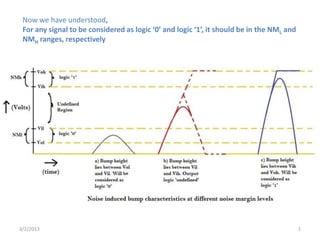
  • 1. Now we have understood, For any signal to be considered as logic ‘0’ and logic ‘1’, it should be in the NML and NMH ranges, respectively 3/2/2013 1
  • 2. Now we have understood, For any signal to be considered as logic ‘0’ and logic ‘1’, it should be in the NML and NMH ranges, respectively Now, let us understand the factors affecting the voltage levels to vary from this range 3/2/2013 2
  • 3. Ideal Switching Activity Actual Switching Activity Switching Activity of a Device is one of the factors which affects the voltage levels of Input/Output signals
  • 4. Vdd Poly Gate PMOS – P Diff In Out NMOS – N Diff Vss Lets understand the internal process while Switching Activity happens in a Device
  • 5. Vdd Poly Gate PMOS – P Diff In Out NMOS – N Diff Vss PMOS NMOS Consider the MOS device, to understand the actual scenario
  • 6. PMOS NMOS Let’s revise MOS device characteristics
  • 17. MOS device characteristics G Vgs S D NMOS Vgs is the Voltage between gate and source
  • 18. MOS device characteristics G Vgs S D NMOS
  • 19. MOS device characteristics G Vgs Vgs < VT (Threshold Voltage) S D S D NMOS If Vgs is less then VT , the NMOS will act as Open Switch
  • 20. MOS device characteristics G Vgs Vgs > VT (Threshold Voltage) S D S D NMOS If Vgs is greater then VT , the NMOS will act as Closed Switch
  • 21. MOS device characteristics G Vgs Vgs > VT S D S D NMOS
  • 22. MOS device characteristics G Vgs Vgs > VT S D S D NMOS When MOSFET is ‘ON’, it can be modeled as a ‘Resistor’ with switch closed
  • 23. MOS device characteristics G Vgs Vgs > VT S D S D NMOS When MOSFET is ‘ON’, it can be modeled as a ‘Resistor’ with switch closed When MOSFET is ‘OFF’, it can be modeled as an ‘open switch’
  • 24. When MOSFET is ‘ON’, it can be modeled as a ‘Resistor’ with closed switch
  • 25. When MOSFET is ‘ON’, it can be modeled as a ‘Resistor’ with switch closed PMOS acts as Logic ‘0’ NMOS acts as Logic ‘1’
  • 26. When MOSFET is ‘ON’, it can be modeled as a ‘Resistor’ with switch closed PMOS acts as Logic ‘0’ NMOS acts as Logic ‘1’ When MOSFET is ‘OFF’, it can be modeled as an ‘open switch’
  • 27. When MOSFET is ‘ON’, it can be modeled as a ‘Resistor’ with switch closed PMOS acts as Logic ‘0’ NMOS acts as Logic ‘1’ When MOSFET is ‘OFF’, it can be modeled as an ‘open switch’ PMOS NMOS PMOS acts as Logic ‘1’ NMOS acts as Logic ‘0’
  • 28. Vdd In Out Vss Input Switching from logic ‘1’ to logic ‘0’
  • 29. Vdd In Out Vss Input Switching from logic ‘1’ to logic ‘0’ NMOS is turning ‘OFF’
  • 30. Vdd In Out Vss Input Switching from logic ‘1’ to logic ‘0’ NMOS is turning ‘OFF’ PMOS is turning ‘ON’
  • 31. Input Switching from logic ‘1’ to logic ‘0’
  • 32. Input Switching from logic ‘1’ to logic ‘0’ NMOS is turning ‘OFF’
  • 33. Input Switching from logic ‘1’ to logic ‘0’ NMOS is turning ‘OFF’ PMOS is turning ‘ON’
  • 34. Input Switching from logic ‘1’ to logic ‘0’ NMOS is turning ‘OFF’ PMOS is turning ‘ON’ Vdd In Out Vss
  • 35. Input Switching from logic ‘1’ to logic ‘0’ NMOS is turning ‘OFF’ PMOS is turning ‘ON’ Vdd Vdd R In Out Out Vss Vss Replace PMOS as resistor and NMOS by open switch.
  • 36. Input Switching from logic ‘1’ to logic ‘0’ NMOS is turning ‘OFF’ PMOS is turning ‘ON’ Vdd Vdd R R Out Out CL Vss Vss Connect Capacitor on output end.
  • 37. Input Switching from logic ‘1’ to logic ‘0’ NMOS is turning ‘OFF’ PMOS is turning ‘ON’ Vdd R Out CL Vss Consider Capacitor is charged when Vdd is applied.
  • 38. Input Switching from logic ‘1’ to logic ‘0’ NMOS is turning ‘OFF’ PMOS is turning ‘ON’ Vdd R Out CL Vss Consider Capacitor is charged up to Vdd
  • 39. Input Switching from logic ‘1’ to logic ‘0’ NMOS is turning ‘OFF’ PMOS is turning ‘ON’ Vdd R Out CL Vss
  • 40. Summary Vdd Vdd R In Out Out CL Vss Vss
  • 41. Summary Vdd R Out CL Vss Lets convert the area within dotted lines into closed loop circuit.
  • 42. Summary Vdd R R Out Vdd CL CL Vss Lets convert into closed loop circuit.
  • 43. Summary Vdd R R Out Vdd CL CL Vss Lets convert into closed loop circuit.
  • 44. Summary Capacitor Models R Vdd CL
  • 45. Summary Capacitor Models R Uncharged Cap + 0V short - Vdd CL + + Charged Cap V VO - O - + Fully Charged Cap Open circuit -
  • 46. Summary Waveforms R Vdd CL
  • 47. Summary Waveforms Vdd R Vdd CL
  • 48. Summary Waveforms Vdd R VCL Vdd CL
  • 49. Summary Waveforms Vdd R VCL Vdd CL VR
  • 50. Summary Waveforms Vdd R VCL Vdd CL VR I = V/R
  • 51. Summary Waveforms Vdd R VCL Vdd CL VR I = V/R IR
  • 52. Summary Waveforms Vdd R VCL Vdd CL VR I = V/R Ipeak IR
  • 53. So what can we conclude!!!
  • 54. So what can we conclude!!! A capacitor needs at least Ipeak amount of current
  • 55. So what can we conclude!!! A capacitor needs at least Ipeak amount of current Ipeak IR
  • 56. So what can we conclude!!! A capacitor needs at least Ipeak amount of current Ipeak IR To get charged upto Vdd voltage
  • 57. So what can we conclude!!! A capacitor needs at least Ipeak amount of current Ipeak IR To get charged upto Vdd voltage VCL
  • 58. So what can we conclude!!! A capacitor needs at least Ipeak amount of current Ipeak IR To get charged upto Vdd voltage VCL And, the output of inverter, is recognized as logic ‘1’
  • 59. So what can we conclude!!! A capacitor needs at least Ipeak amount of current Ipeak IR To get charged upto Vdd voltage VCL And, the output of inverter, is recognized as logic ‘1’
  • 60. And, the output of inverter, is recognized as logic ‘1’
  • 61. And, the output of inverter, is recognised as logic ‘1’ What does this mean????
  • 62. And, the output of inverter, is recognised as logic ‘1’ What does this mean???? It means that the voltage across capacitor Vpeak VCL
  • 63. And, the output of inverter, is recognised as logic ‘1’ What does this mean???? It means that the voltage across capacitor Vpeak VCL Lies in NMH level of noise margin graph
  • 64. Vdd VOH NMH VIH Noise Margin High NMH = VOH - VIH NML = VIL - VOL VIL NML Noise Margin High VOL 0