
Recommended
More Related Content
Similar to Microwave PPT.ppt
Similar to Microwave PPT.ppt (20)
Recently uploaded
Recently uploaded (20)
Microwave PPT.ppt
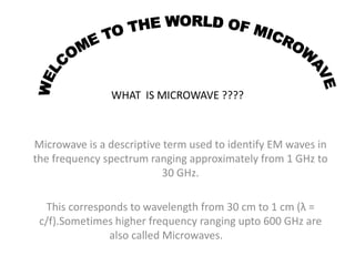
- 1. WHAT IS MICROWAVE ???? Microwave is a descriptive term used to identify EM waves in the frequency spectrum ranging approximately from 1 GHz to 30 GHz. This corresponds to wavelength from 30 cm to 1 cm (λ = c/f).Sometimes higher frequency ranging upto 600 GHz are also called Microwaves.
- 2. APPLICATION Communication • UHF TV • Microwave Relay • Satt. Comm • Tropo Sctter Comm • Mobile Radio • Telemetry RADAR • Search • ATC • Navigation • Radar Altimeter • Velocity Measurements EWS ECM ESM ECCM Microwave Heating • Industrial Heating • Microwave oven Industrial,Scientific,Medical • Linear Acclerators • Plasma Containment • Radio Astronomy • Whole body cancer theraphy
- 3. MAXWELL EQUATION • Ampere’s Law ∫H.dl= I I is the surface Integral of Conduction current density JT over the bounded area by the path of Integration The Total current Density JT = J + ∂[D]/∂t ∫ H. dl = ∫s (J + ∂/∂t[D]) . ds By applying Strokes Theorem ∫ H. dl = ∫s (Δ X H).ds Hence Δ X H = J + ∂/∂t[D]
- 4. MAXWELL EQUATION Faraday’ Law • V= - = ∫E.dl Φ= • ∫E.dl = - ∂/∂t ∫s B.ds By applying Strokes Theorem ∫ E. dl = - ∂/∂t ∫s (Δ X E).ds (Δ X E) = - ∂/∂t [B] ∫s B.ds
- 5. Gauss’s Law • In Its Basic form • ∫D.ds = ∫v ρdv • Lt ∫ (D.ds)/dv = Δ.D dv 0 • Δ.D= ρ • In case of magnetic field the surface integral over of B over a closed surface is zero. This is because a magnetic field has neither a source nor a sink. • Therefore Δ.B = 0
- 6. Wave Equation We assume here the field vector vary with respect to time t in a sinusoidal manner Then we have E = E0 exp (jωt) Therefore we have ∂E/ ∂t = jωE Therefore we have ∂/∂t = jω Similar way ∂2/∂t2 = -ω2 Now consider a medium which does not contain any free charges and is also non conducting, for example free space or air.Then we have ρ = 0 , σ=0 Therefore maxwell ‘s 1st & 2nd Eqns give the following form Hence Δ X H = J + ∂/∂t[D] = σ E + ∂/∂t (εE) = jωεE Δ X E = - ∂/∂t [B] = - jωμH Taking the curl of 2nd Eqn We have Δ X Δ X E = ω2 μεE From Maxwell 3 rd Eqn We have Δ.D= ρ = 0 We know from vector Analysis Δ X Δ X E = ∆ . (∆.E) - ∆2E Therefore ∆ . (∆.E) - ∆2E = ω2μεE Therefore ∆.E = 0 So ∆2E = -ω2μεE Similar way ∆2H = - ω2 μεH
- 7. Wave Equation Therefore maxwell ′s 1st & 2nd Eqns give the following form Hence Δ X H = J + ∂/∂t[D] = σ E + ∂/∂t (εE) = jωεE ..(1) Δ X E = - ∂/∂t [B] = - jωμH…….(2) Taking the curl of 2nd Eqn We have Δ X Δ X E = ω2 μεE From Maxwell 3 rd Eqn We have Δ.D= ρ = 0 We know from vector Analysis Δ X Δ X E = ∆ . (∆.E) - ∆2E Therefore ∆ . (∆.E) - ∆2E = ω2μεE Therefore ∆.E = 0 So ∆2E = -ω2μεE Similar way ∆2H = - ω2 μεH
- 8. Wave Equation in other form • ∆2E = 1/c2 ∂2E/∂t2 • ∆2H = 1/c2 ∂2H/∂t2 • Where c is velocity of light in vaccum. • These two Eqns represents wave propagating through free space with a velocity equal to that of light and are also known as HELMHOLTZ Equation.
- 9. TEM/ TE/ TM/ HE Modes EZ,HZ E y , H y When Ez = 0 =Hz, mode is called TEM, When only Ez = 0 it is called TE, When only Hz=0 It is called TM, When Ez≠0,Hz≠ 0 , It is called HE/EH Mode.
- 10. Relationship • In rectangular co- ordinate system • ∆2E = ∂2E/∂x2 + ∂2E/∂y2 + ∂2E/∂z2 • In Cylindrical co ordinate system ∆2E = ∂2E/∂ρ2 +(1/ρ) ∂E/∂ρ +(1/ρ2) ∂2E/∂φ2 + ∂2E/∂z2 Δ X E can be written as Δ X E can be written as In rectangular Co-ordinate In Cylindrical Co-ordinate i j k ∂/∂x ∂/∂y ∂/∂z Ex Ey Ez (1/ρ) uρ uɸ (1/ρ) uz ∂/∂ρ ∂/∂ɸ ∂/∂z Eρ Eɸ Ez
- 11. A conclusion • If a wave travelling along positive z direction then the wave Eqn can be represented as • ∆2Ez = - ω2μεEz ∆2Hz = - ω2 μεHz Then its components that is plane wave is represented by Ez= Eoz exp (-γz) Where γ =α+jβ Therefore ∂/∂z = - γ ∂2/∂z2 = γ2
- 12. Some basic definition of Tx Lines • Characteristics Impedance = Zo =[(R+jωL)/ (G + jωC)]½ • The Reflection Coefficient ρ = (ZL-Zo)/(ZL+Zo) • VSWR S = (1+ I ρI)/(1- IρI) • Attn Loss = 10 log10 [(Ei-Er)/Ei] • Reflection Loss = 10 log10 [Ei/(Ei-Er)] • Transmission Loss = 10 log10(Ei/Er) • Return Loss = 10 log10 Ei/Er= -20 log10 IρI • Insertion Loss = 10 log10E1/E2
- 13. Waveguide • A waveguide consists of hollow metallic tube of rectangular or circular shape used to guide an EM wave. • In waveguides the E- fields & H- fields are confined to a space within the guide. Thus no power is lost through radiation and even the Dielectric Loss is negligible, since the guide are normally air-filled. • It is possible to propagate several modes within the waveguide. • Dominant Mode :- The dominant mode in particular waveguide is the mode having the lowest cutoff frequency. • It is advisable to choose the dimension of a guide in such a way that, for a given input signal only the energy of dominant mode can be transmitted through the guide.
- 15. Soln to the waveguide Equation The process of solving waveguide Eqn may involve three steps: • The desired wave equation are written in the form of either rectangular or cylindrical co-ordinate. • The boundary condition are then applied to the wave equation set up in the above. • The resultant eqn usually are in the form of partial differential eqn in either freq. or time domain.
- 16. Solution of wave Equation in Rectangular co-ordinates The E Field and H field in frequency domain are given by ∆2Ez = - ω2μεEz = γ2 Ez ∆2Hz = - ω2 μεHz = γ2 Hz Where γ2= [jωμ(σ+ jωε)] The Rectangular components of E & H satisfy the complex scalar wave Eqn or Helmhotz Equation. i.e. ∆2 ϕ = - ω2με ϕ= γ2 ϕ This can be written as ∂2ɸ/∂x2 + ∂2ɸ/∂y2 + ∂2ɸ/∂z2 = γ2 ϕ. This is PDE of ϕ in 3D Soln By the use of Separation of variables
- 17. Solution of wave Equation in Rectangular co-ordinates • ϕ = X(x) Y(y) Z(z) • Then We have • (1/X)d2X/dx2 + (1/Y)d2Y/dy2+ (1/Z)d2Z/dz2 = γ2 • Since the sum of three terms on LHS is a constant and each term is independently variable, It follows that each term must be equal to constant • Let us take -κ2 x -κ2 y -κ2 z = γ2 • d2X/dx2 = -κ2 xX • d2Y/dy2 = -κ2 y Y • d2Z/dz2 = -κ2 z Z
- 18. Solution of wave Equation in Rectangular co-ordinates • The solution of the above three Equations • X = A sin(κxx ) + B cos(κxx ) • Y = C sin(κyy) + D cos(κyy) • Z = E sin(κzz) + F cos(κzz) • The total Solution of the Helmhotz Eqn in Rec. Co- ordinate Φ = [ A sin(κxx ) + B cos(κxx )]. [C sin(κyy) + D cos(κyy)][E sin(κzz) + F cos(κzz)]
- 19. Soln of wave Eqn • The propagation of wave in the guide is conventionally assumed in the +ve direction. It should be noted that the propagation constant γg in the guide differs from the intrinsic prop. constant γ of the dielectric. Let γg 2 = γ2+ κ2 x+ κ2 y = κ2 c+ γ2 κc = (κ2 x+ κ2 y) ½ κc Called cut off wave number. For a lossless dielectric γ2 = - ω2 με Then γg 2 = κ2 c+ γ2 γg 2 = - ω2 με + κ2 c γg=√(ω2 με - κ2 c) There are three cases for the propagation constant in the guide------ I : There will be no wave propagation in the guide if ωc 2 με = κ2 c, This is the critical condition for cut off propagation. Therefore the cut- off frequency is given by fc = (1/2π √εμ) κc
- 20. Solution of wave Equation in Rectangular co-ordinates Case II : The wave will be propagating in the guide if ωc 2 με ˃ κ2 c, and γg = (+-) jβg = (+-) jω √εμ √[1-(fc/f)2] This means that the operating freq.must be above the cut- off freq. in order to propagate in the guide. CaseIII. The wave will be atteneuted if ωc 2 με ˂ κ2 c and γg = α g = (+-) ω √εμ √[(f/fc)2-1] This means that if the operating is below the cut-off freq, the wave will decay exponentially wr t a factor of -α gz and there will be no wave propagation becoz the constant is a real quantity. Therefore the soln of the Helmhotz Eqn in Rec. co-ordinate Φ = [ A sin(κxx ) + B cos(κxx )]. [C sin(κyy) + D cos(κyy)].[E sin(κzz) + F cos(κzz)] exp (- jβgz)
- 21. RWG Transmission
- 22. RWG Transmission • Typically the di-electric is air. • We have • ∂2E/∂x2 +∂2E/∂y2 + ∂2E/∂z2 = γ2 E. • ∂2E/∂x2 +∂2E/∂y2 + ∂2E/∂z2 = - ω2 με E • ∂2E/∂x2 +∂2E/∂y2 + ∂2E/∂z2 + ω2 με E=0 • For lossless propagation in the +ve z direction all the three components must have an exp (- jβgz) functional dependence. Therefore • ∂2E/∂x2 +∂2E/∂y2 +(ω2 με - βg 2 ) E=0 • ∂2E/∂x2 +∂2E/∂y2 + κ2 c E=0 as ω2 με - βg 2 = κ2 c • Similarly • ∂2H/∂x2 +∂2H/∂y2 + κ2 c H=0 • Hence We will have total six components in x, y, z direction.
- 27. TE Mode solution • The above condition require that B= 0, κx= mπ/a, D=0 and κy=nπ/b Where m & n are the +ve integer. Hence We have Hz = AC exp (- jβgz) cos (nπ/b)x cos (mπ/a)y = H0 exp (- jβgz) cos (nπ/b)y cos (mπ/a)x This eqn represents all possible solutions of Hz for TE modes in RWG. The other components can be obtained from the original curl eqn. For TE waves (Ez=0) the phasor form of these equation reduces to (i) βgEy = ωμHx (ii) ∂Hz/∂y+jβHy= jωεEx (iii) βgEx = ωμHy (iv) jβgHx + ∂Hz/∂x = - jωεEy (v) ∂Ey/∂x - ∂Ex/∂y = - jωμHz (vi) ∂Hy/∂x- ∂Hx/∂y = 0
- 28. RWG • With some algebraic manipulation, all field components can be expressed in terms of Hz • Ex = - (jωμ/ κ2 c) ∂Hz/∂y Ey = (jωμ/ κ2 c) ∂Hz/∂x Ez= 0 Hx = - (jβg/ κ2 c)∂Hz/∂x Hy= - (jβg/ κ2 c)∂Hz/∂y Hz= = H0 exp (- jβgz) cos (nπ/b)y cos (mπ/a)x Substituting the value of Hz in the above Equation, We have, Ex = - (jωμ/ κ2 c) H0(nπ/b) exp (- jβgz) sin (nπ/b)y cos (mπ/a)x = E0x sin (nπ/b)y cos (mπ/a)x exp (- jβgz) Similar way Ey =Eoy cos (nπ/b)y sin (mπ/a)x exp (- jβgz) Ez=0 Hx = Hxo cos (nπ/b)y sin (mπ/a)x exp (- jβgz) Hy = Hoy sin (nπ/b)y cos (mπ/a)x exp (- jβgz) Hz= = H0 exp (- jβgz) cos (nπ/b)y cos (mπ/a)x
- 29. Cut off Frequency ( Wave as High pass Filter) • We know that • κ2 c = γg 2 + ω2 με = (κ2 x+ κ2 y) =( mπ/a)2 +(nπ/b)2 • γg 2 = ( mπ/a)2 +(nπ/b)2 - ω2 με • γg = √([( mπ/a)2 +(nπ/b)2 - ω2 με] • At lower freq. ( mπ/a)2 +(nπ/b)2 ˃ ω2 με • γg becomes real and +ve and the wave is completely attenuated and there is no phase change. Hence the wave can not propagate. • However at higher freq, ( mπ/a)2 +(nπ/b)2 ˂ ω2 με, γg becomes imaginary and propagation constant β changesand wave propagates. • At the transition, γg becomes Zero and the propagation just starts. • The frequency at which the γg just becomes zero is defined as Cut-off freq.( Threshold Freq.) fc.
- 30. RWG • However at higher freq, ( mπ/a)2 +(nπ/b)2 ˂ ω2 με, γg becomes imaginary and propagation constant β changes and wave propagates. • At the transition, γg becomes Zero and the propagation just starts. • The frequency at which the γg just becomes zero is defined as Cut-off freq. ( Threshold Freq.) fc.
- 31. Cut off Frequency ( Wave Guide as High pass Filter) • γg = √([( mπ/a)2 +(nπ/b)2 - ω2 με] • 0 = √([( mπ/a)2 +(nπ/b)2 - ωc 2 με] • From this it can be written as • fc= (c/2) √([( m/a)2 +(n/b)2 ] as c= 1/√(εμ) • Cut off wave length = λc = c/ fc= c/(c/2) √([( m/a)2 +(n/b)2 ] • = 2/ √([( m/a)2 +(n/b)2 ] • All wavelength greater than λc are atteneuated and less than will be propagated
- 34. • Guided WavelengtSome important definition • h: (λg) : It is defined as the distance travelled by the wave in order to undergo a phase shift of 2π It is related by the Radians.It is related to the phase constant by the relation λg=2π/ βg Phase Velocity: (vp): In a waveguide vp the velocity of propagation is the product of λg and f. But the speed of light is equal to the product of λo and f. This Vp is greater than than the speed of light since λg ˃ λo. This is contradicting since no signal can travel faster than light. However the wavelength in the guide is the length of the cycle and vp represents the velocity of phase. In fact it is defined as the rate at which the wave chages its phase in terms of guided wavelength. i.e. vp= λg . f = (2πf . λ g)/2π = (2πf .)/2π/ λ g = ω/ βg Since no intelligence or modulation travel at this velocity ‘ this velocity is known as Phase Velocity.
- 35. Some important definition • Group Velocity (vg): If there is modulation in the carrier, the modulated envelope actually travels at velocity slower than that of carrier alone and of course slower than speed of light. The velocity of modulation envelope is called the Gp. Velocity. This happens when a modulated signal travels in a waveguide, the modulation goes on slipping backward w r t the carrier. It is defined as the rate at which the wave propagates through the waveguide and is given as vg= dω/dβ
- 36. Expression for the Phase Velocity • As we know vp= ω/ βg • We also know κ2 c = γg 2 + ω2 με = (κ2 x+ κ2 y) =( mπ/a)2 +(nπ/b)2 γg = α g +jβg For the wave to propagate γg = (+-)jβg γg 2 = [(+-)jβg]2 = -β2 g = ( mπ/a)2 +(nπ/b)2 - ω2 με At f= fc, ω = ωc, γg = 0 There fore ωc 2 με = ( mπ/a)2 +(nπ/b)2 Therefore γg 2 = [(+-)jβg]2 = -β2 g = ωc 2 με - ω2 με β2 g = ω2 με -ωc 2 με βg =√( ωc 2 με - ω2 με) = √( με) √(ω2 -ωc 2 ) Therefore vp= ω/ βg = ω/ [√( με) √(ω2 -ωc 2)] = c/ (√[1-(fc/f)2]) = c/(√[1-(λ0 / λc)2]
- 37. Expression for the Gp Velocity • vg= dω/dβg • As we know βg = √( με) (ω2 -ωc 2 ) then differentiating dβg/ dω = 1/[2(√( με) (ω2 -ωc 2 )] . 2 ωμε = √( με) / √[1-(fc/f)2] • Therefore vg= dω/dβ = √[1-(fc/f)2]/ √( με) = c √[1-(fc/f)2] = c √[1-(λ0/ λc)2 • Therefore we can conclude that vg vp = c2
- 38. Relation between λ0, λc, λg • vp= λg. f = (λg / λ0) . c • vp = c/(√[1-(λ0 / λc)2] From this two equation we have (λg / λ0) . c = c/(√[1-(λ0 / λc)2] After some manipulation We can write 1/ λ2 0 = (1/λ2 c)+ (1/λ2 g) From this We can write λg = (λ0)/(√[1-(λ0 / λc)2] For the case of wave guide with constant εr, λg = (λ0)/(√[εr -(λ0 / λc)2] and λg dielectric = (λg air)/√(εr) Since εr is always greater than 1 and εr˃ εdielectric hence frequency less than cut-off frequency can pass through the wave guide
- 40. TM modes solution • From the boundary condition require that B= 0, κx= mπ/a, D=0 and κy=nπ/b Where m & n are the +ve integer. Hence We have Ez = E0z sin (nπ/b)y sin (mπ/a)x exp (- jβgz) This eqn represents all possible solutions of Hz for TE modes in RWG. The other components can be obtained from the original curl eqn. For TM waves (Ez=0) the phasor form of these equation reduces to (i) ∂Ez/∂y+jβgEy=- jωμ Hx (ii) jβgEx + ∂Ez/∂x = jωμHy (iii) ∂Ey/∂x - ∂Ex/∂y =0 (iv) βgHy = ωεEx (v) -βgHx + ∂Hz/∂x = ωεEy (vi) ∂Hy/∂x - ∂Hx/∂y = - jωεEz
- 41. TM modes solution • These equation can be solved simultaneously for Ex, Ey, Hx, Hy in Terms of Ez and Hz • Ex = - (jβg/ κ2 c)∂Ez/∂x • Ey = - (jβg/ κ2 c) ∂Ez/∂y • Ez= = E0z exp (- jβgz) sin(nπ/b)y sin (mπ/a)x • • Hx = (jωε/ κ2 c) ∂Ez/∂y Hy = - ((jωε/ κ2 c))∂Ez/∂x • Hz= 0
- 42. Ex = E0x sin (nπ/b)y cos (mπ/a)x exp (- jβgz) Ey =Eoy cos (nπ/b)y sin (mπ/a)x exp (- jβgz) Ez= E0z sin (nπ/b)y sin (mπ/a)x exp (- jβgz) Hx = Hox cos (nπ/b)y sin (mπ/a)x exp (- jβgz) Hy = Hoy sin (nπ/b)y cos (mπ/a)x exp (- jβgz) Hz= = 0
- 43. TM & TE modes in RWG Various TMmn modes: • (i) TM00 Modes : If m=0 n=0 , We see all the components are vanishing , Hence We will have trival solution. • (ii) TM01 Modes: Again all the field components vanish • (iii) TM10 Modes: Even now all are vanishing • (iv) TM11 Modes: Now all the components Exist and for all other values of m,n , the components exists. Various TEmn Modes: Similarway (i) TE00 Modes: TE00 does not exist. • (ii) TE01 Modes : Ex Hy Exist, Hx=Ey=0 • (iii) TE10 Modes: Ex = Hy =0, Hx&Ey Exist • (iv) TE11 Modes: All the components Exist •
- 44. Dominant & degenerate Modes • Dominant mode is that mode for which the cut off wavelength assumes a max value. • Cut off wave length = λcm,n = c/ fc= c/(c/2) √([( m/a)2 +(n/b)2 ] • = 2/ √([( m/a)2 +(n/b)2 ] • For (i) TE01 Modes : λc0,1 = 2b • (ii) TE10 Modes: λc1,0 = 2a • (iii) TE11 Modes: λc1,1 = 2ab/√(a2 +b2) • Of these λc1,0 has max. value since a is the largest. Hence TE10 Mode is the dominant mode for RWG. • Degenerate modes : Whenever two or more modes have the same cut-off freq, they are said to be degenerate modes. • In a particular waveguide the corresponding TEmn & TMmn modes are always degenerate. In square guide the TEmn, TEnm, TMmn, TMnm modes form a foursome of degeneracy.
- 45. Wave Impedance Zz in TM and TE Waves. • Wave Impedance is defined as the ratio of the strength of electric field in one transverse direction to the strength of the magnetic field along the other transverse direction. • Wave Impedance for a TM wave in RWG For a TM wave Hz = 0 and γg =jβg Zz ™ = Ex / Hy = [- (jβg/ κ2 c)∂Ez/∂x]/[- ((jωε/ κ2 c))∂Ez/∂x] = βg/ ωε = √(ω2 με -ωc 2 με)/ ωε = √(μ/ε) √ [1-(λ0 / λc)2] For air, √(μ/ε) = 377 Ω = η Therefore Zz ™ = η √ [1-(λ0 / λc)2] Similarway Zz TE = η /√ [1-(λ0 / λc)2], This shows that wave impedance for TE mode is always greater than η
- 52. Poynting Theorem • At what rate will electromagnetic energy be transmitted through free space or any medium, be stored in the E field or M field, and be dissipated as heat? • From the standpoint of complex power in terms of complex field vectors, the time average of any two complex vectors is equal to the real part of the product of one complex vector multiplied by the complex conjugate of the other vectors. Hence • < P> = <ExH> = (½) Re (ExH*)
- 53. Poynting Theorem • It is neceessary to define a complex poynting vector as P => = (½) Re (ExH*) • Maxwell Equation in frequency domain • ∆XE = -jωμH • ∆XH = J+jωεE • (∆XE).H* = -jωμH. H* • (∆XH*).E = (J*-jωεE*).E • Substracting
- 54. Poynting Theorem • E.(∆XH*)- H*.(∆XE) =E.J* -jω[ε|E|2-.μ|H|2] • -∆.(ExH*) = E.J* -jω[ε|E|2-.μ|H|2] • (½)∆.(ExH*) = -(½)E.J* +(½) jω[ε|E|2-.μ|H|2] • After putting J= (Jo*+σE) and P=(½) (ExH*) Manipulating We have -(½)E.Jo*= (½) σE. E*+(½) jω[(½)μH.H*-(½)εE.E*] + ∆.P Integrating over a volume and application of Gauss’s theorem We have ∫(½)E.Jo*= ∫(½) σE. E*+∫(½) jω[(½)μH.H*-(½)εE.E*] +∫ ∆.P
- 55. Poynting theorem • ½ σ║E2║ = σ˂║E2║˃ is the time average dissipated power. • ¼ μH.H* = ½ μ ˂║H2║˃ = wm is the time average magnetic stored energy • ¼ εE.E* = ½ ε ˂║E2║˃ = we is the time average electric stored energy • - ½ E.J0* = The complex power impressed by the source Jo in the field • Pin = - ʃv ½ (E.J0*)dv =The total complex power impressed by the source J0 within the region.
- 56. Poynting theorem • ˂Pd˃ = ʃv ½ σ║E2║dv be the time average dissipated as heat inside the region. • Wm-We = ʃv (wm -we ) dv be the difference between time av. Mag. And elec field stored within the region. • Ptr = ∫ P.ds be the transmitted power from the region. • The complex poynting theorem can be written as • Pin= ˂Pd˃ +j2ω ˂ Wm-We ˃ + Ptr
- 57. Power transmission through RWG • The power transmitted a RWG (assuming the waveguide is infinitely long and no reflection are coming from load end) Ptr = ∫ P.ds = ∫ (E X H*).ds For a lossless dielectric, the time av. Power flow through a RWG is given by Ptr = 1/(2Zz) ʃa║E2║da = (Zz)/2 ʃa║H2║da Where Zz= Ex / Hy = -Ey/ Hx Where ║E║2 = ║Ex║2+ ║Ey║2 and ║H║2= ║Hx║2 + ║Hy║2 For the TEmn the av power transmitted through a RWG is Ptr = [√ [1-(λ0 / λc)2] / (2η)] x [ʃ0 a ʃ0 b[║Ex║2+ ║Ey║2]dx dy] For the TMmn the av power transmitted through a RWG is Ptr = 1/ [√ [1-(λ0 / λc)2] / (2η)] x [[ʃ0 a ʃ0 b ║Ex║2+ ʃa║Ey║2]dx dy]
- 58. Power Losses in RWG • Losses in Dielectric • Losses in the guided wall • Power loss in Dielectric For low loss dielectric (σ ˂˂με), The propagation constant for a plane wave travelling in unbounded lossy dielectric is given by α = (σ/2) √(μ/ε) =ησ/2 The attn caused by the low loss dielectric in RWG is given by αg =[ησ/2]/ [√ [1-(λ0 / λc)2] for TE modes αg =[ησ/2]x [√ [1-(λ0 / λc)2] for TM modes
- 59. Power Loss es in the guide wall • The E & H field propagate through a lossy waveguide, their magnitudes • ║E║ = ║Eoz║ exp ( - αgz) • ║H║ = ║Hoz║ exp ( - αgz) • It is interesting to note that, for a low loss guide, the time av. Power flow decreases proportionally to exp(( - 2αgz) • Hence Ptr = (Ptr + Ploss) exp(( - 2αgz) • For Ptr ˂˂ Ploss and 2αgz ˂˂1, • • (Ploss/ Ptr) + 1 = 1+ 2αgz • Finally αg= PL/ 2Ptr PL is the loss per unit length
- 60. Power Losses in the guide wall • Since the E field and H field established at the surface of low loss guide wall decay exponencially wrt the skin depth while the waves progress in the wall, it is better to define a surface resistance of the guide wall as • Rs = ρ/δ = 1/(σδ) = (αg)/σ = √ (πfμ)/σ Ω/Square • The power loss/ lentgh of guide • PL = (Rs/2) ʃ ║Ht║2 ds Ht is the tangential components of the H field • αg= [ Rs ʃs ║Ht║2 ds]/[2Zz ʃa║H║2da] Where ║H║2 = ║Hz║2+ ║Ey║2 and ║Ht║2= ║Htx║2 + ║Hty║2
- 61. TE10 mode in RWG • An air field waveguide with a cross section 2x1 cms transport energy in the TE10 mode at the rate of 0.5 hp. The impressed frequency is 30 GHz. What is the peak value of the E- Field occuring in the guide? • SOLUTION • (1)Find the βg • (2) The power delivered in the z direction by the guide is P = Ptr =Re [1/2 ʃ0 b ʃ0 a (E X H*)]dx.dy uz • Put the value of Ey & Hx and get the answer.
- 62. Characterisrics of standard Waveguide • The side dimension of RWG designated as EIA WR (90) by Electronic Industry association • For Example The X band frequencies the outside dimension of a RWG is 2.54 cm wide and 1.27 cm high and its inside dimension are 2.286 and 1.016 cms respectively
- 64. CWG
- 65. CWG x r a f z
- 66. CWG • In cylindrical co-ordinate system, the Helmhothz Eqn can be written as • (1/r) ∂/∂r(r ∂Ez/∂r) + (1/r2) ∂2Ez /∂Φ2 = -κ2 c Ez • (1/r) ∂/∂r(r ∂Hz/∂r) + (1/r2) ∂2Hz /∂Φ2 = -κ2 c Hz
- 67. CWG TE modes In this case Ez = 0 and Hz not equal to 0. For Propagation in + ve z direction We have Hz = Hz* exp (-jβz) Hz* is the fn of r and Φ only. There the Equation becomes • (1/r) ∂/∂r(r ∂ Hz* /∂r) + (1/r2) ∂2 Hz* /∂Φ2 = -κ2 c Hz* Again use the separation of variable…….. i.e. Hz* = R Ψ Then the Equation becomes d2R/dr2 + (1/r) dR/dr +[κ2 c- (n2/r2)] R = 0 And d2 Ψ /dΦ2 + n2 Ψ =0 n2 is a constant
- 68. CWG • The solution of the Equation R= A Jn(κcr) + B Nn (κcr) Ψ = C cos (n Φ) +D sin (n Φ) Since the field must remain finite at r=0, the Nn term must be excluded and therefore B=0. Since the field, and Hence Ψ must be single valued, n is restricted to integer value. Finally, one of the two Ψ terms can be eliminated as both of this leads to same field pattern except that one is rotatiing 90o in Φ direction. Setting D=0 yields Hz* = Ho Jn(κcr) cos (n Φ) Where Ho = AC is an arbitary amplitude.
- 69. CWG • At r= a, the boundary condition requires that ∂Hz/∂r= 0, which means J'n(κca) =0 The m th root of this equation is designated by q'nm and thus q'nm = κca several roots value are available The right hand side table gives the different value of q'mn in TEmn modes. m n 1 2 0 3.832 7.016 1 1.841 5.331 2 3.054 6.706
- 70. CWG • Now The Equation for Hz may be written as Hz= Hz* exp (-jβz) = Ho Jn(κcr) cos (n Φ) exp (-jβz) Where κc= q'mn/a The remaining field equation can be obtained from original curl Equation. For TE waves The phasor form of the equation are (1) βgEΦ= -ωμHr (2) (1/r) (∂Hz/∂Φ) + jβgHΦ=jωεEr (3) βgEr = ωμ HΦ (4) jβgHr +∂Hz/∂r= - jωεEΦ (5) (1/r) {∂ (rEΦ)/∂r - ∂(Er)/∂Φ}= -jωμHz (6) (1/r) {∂ (rHΦ)/∂r - ∂(Hr)/∂Φ}= 0 These equation can be solved for EΦ ,Hr ,HΦ,Er in terms of Hz and Ez.
- 71. CWG (1) EΦ= =(-jωμ)/ -κ2 cr ∂(Hz)/∂r (2) HΦ= (-+) EΦ/ ZTE (2) Er =(-jωμ)/ -κ2 cr ∂(Hz)/∂Φ (4) Hr = (+-) HΦ / ZTE By substituting the Hz in the above Equation We have the different field components. Er =(-jωμ)/ -κ2 cr ∂(Hz)/∂Φ = jHo (nωμ)/ (κ2 cr) Jn(κcr) sin (n Φ) X exp (-jβz) EΦ=jHo (ωμ)/ (κc) J'n(κcr) cos (n Φ) X exp (-jβz) Er = (+-) HΦ / ZTE HΦ= (-+) EΦ/ ZTE Where κc= q'mn/ a and Zz TE = η /√ [1-(λ0 / λc)2
- 72. CWG • As we know β2 g =(ω2 με - κ2 c) • βg =√(ω2 με - κ2 c) • As we know κc= q‘nm/ a • Therefore , The cut-off wave number of a mode is that mode for which the mode propagation constant vanishes. • Hence 0=β2 g =(ω2 με - κ2 c) κc = ωc √ με = q‘nm/ a The cut off frequency for TE mode in CWG is fc = (1/2π √εμ) κc = (q'mn /2π a √εμ) Therefore λc = 2π a / q‘nm
- 73. CWG • Λc will be maximum if q‘nm • is minimum. • Therefore the value of q‘nm is found to be minimum i.e. 1.841 for n =1, m=1 Hence TE11 is called dominant mode in CWG i.e. λc = 2π a / q‘nm = 2π a / 1.841 m n 1 2 0 3.832 7.016 1 1.841 5.331 2 3.054 6.706
- 74. CWG TM modes qnm for TM modes m n 1 2 0 2.405 5.520 1 3.832 7.016 2 5.135 8.417
- 75. • Q1 Define the Degenerate Modes in CWG `with Example. • Q2 An air field CWG has a radius of 2 cms and is to carry energy at a frequency of 10 GHz. Find all the TEmn and TMmn modes for which energy transmission is possible.
- 76. Ad, Disad, of CWG • It is easier to manufacture • Easier to join • TM01 & TE01 are symmetrical,Hence rotation of polarization can be overcome • TE01 mode in CWG has the lowest attn /unit length of waveguide, Hence suitable for long distance tx. • DISAD……………………………. • Occupy more space • Plane of polarization rotates • Very difficult to separate dominant modes from infinite no. of modes available.
- 77. Application • As a rotating joints in Radars • TE01 mode in CWG has the lowest attn /unit length of waveguide, Hence suitable for long distance tx. • Short and Medium distance broadband comm.( could replace /share coaxial and microwave links)
- 78. Characteristics of Standard CWG • The inner diameter of a CWG is regulated by the freq. of the signal being transmitted. • For example : at X band freq., the inner diameter of a CWG designated as EIA WC (94) by the Electronic Industry Association is 2.383 cm.
- 79. Microwaves Cavities • Cavities, or resonators, are used for storing energy • Used in klystron tubes, band-pass filters and frequency meters • It’s equivalent to a RLC circuit at high frequency • Their shape is that of a cavity, either cylindrical or cubical or Rectangular They serve as key elements in osc,,tuned amplifiers, frequency meters, phase equalizers as well as BPF
- 80. CR • It is a metallic enclosure that confines the EM energy. • The stored E & M energies inside the cavity determine its equivalent inductance and capacitance. • The energy dissipated by the finite conductivity of the cavity walls determine its equivalent resistance. • Example RCR, CCR, Re-Entrant Cavity • A given resonator has a infinite no of modes and each modes corresponds to a definite resonant frequency. • When the frequency of an impressed waveform is equal to a resonant freq, a max amplitude of the standing waves occurs, and the peak energy stored in the E & M Fields are equal. • The mode having the lowest resonant freq. is known as dominant mode.
- 81. CR Its Q is very very high. Q= 2π (energy stored)/(energy Loss per cycle) Unloaded Qu =ωr (energy stored in the resonant circuit)/(Power Loss in the resonant circuit)| at ωr External QE =ωr (energy stored the resonant circuit)/(power Loss in the external circuit)|at ωr Loaded QL =ωr (energy stored in the resonant circuit)/(Total Power Loss)|at ωr
- 82. CR • It can easily proved that (1/ QL) = (1/ QE) + (1/Qu) Therefore We can say QL is a function of the degree of coupling between the resonant circuit and external circuit.
- 83. CR • Hollow metallic enclosure exhibit resonance behavior when excited by an EM field. These enclosures are known as CR and are widely used above 3 GHz. • Typical value of Q ranging from 5000 to 50000 • CR has a infinite no of modes and each modes corresponds to a definite resonant frequency • These can be determined by Maxwell Equation.
- 84. RCR
- 85. RCR
- 86. RCR • The cavity is resonant at freq. where length I is multiple of λg/2 , λg is guided wavelength along Z- axis. • • At certain freq, an E- Field null occur at z=0
- 87. The resonant condition is given by l = p λg/2 • For βl =pπ, the waves adds constructively thus producing the resonant condition
- 88. The resonant condition is given by l = p λg/2 For βl =pπ, the waves adds constructively thus producing the resonant condition
- 89. Field Analysis in TE modes: ∂2Hz/∂x2 +∂2Hz/∂y2 + κ2 c Hz=0 : obtain we where from ) ( ) ( ) ( ) , , ( : Variables of Separation by Solving z Z y Y x X z y x H z z k c z k c z Z y k c y k c Y(y) x k c x k c X(x) z z y y x x sin cos ) ( sin cos sin cos 6 5 4 3 2 1 2 2 2 2 z y x k k k k where Cavity TE Mode to z
- 90. Rectangular CR • TEmnp Boundary Conditions ,b y E ,a x E ,c z H x y z 0 at , 0 0 at 0 0 at 0 From these, we conclude: kx=mπ/a ky=nπ/b kz=pπ/c where c is the dimension in z-axis c y p b y n a x m H H o z sin cos cos
- 91. RCR In TE modes • Substituting the value of kx ky and kz in the first equation we have • [(mπ/a)2 + (nπ/b)2 +(pπ/c)2 - ω2 με] Hz=0 If Hz = 0, all the filed components will vanish and the solution is trival. In order for the field to be non- zero the following condition must hold (mπ/a)2 + (nπ/b)2 +(pπ/c)2 = ωr 2 με fr = [1/(2 √ με)][(m/a)2 + (n/b)2 +(p/c)2]
- 92. Cavity TM Mode to z : obtain we where from ) ( ) ( ) ( ) , , ( : Variables of Separation by Solving z Z y Y x X z y x Ez z k c z k c z Z y k c y k c Y(y) x k c x k c X(x) z z y y x x sin cos ) ( sin cos sin cos 6 5 4 3 2 1 2 2 2 2 z y x k k k k where
- 93. TMmnp Boundary Conditions • From these, we conclude: • kx=mπ/a • ky=n π /b • kz=p π /c • where c is the dimension in z-axis ,c z E E ,a x E ,b y E x y z z 0 at , 0 0 at 0 0 at 0
- 94. Cavity TM Mode to z 2 2 2 2 2 cos sin sin c p b n a m k where c z p b y n a x m E E o z
- 95. Resonant frequency • The resonant frequency is the same for TM or TE modes, except that the lowest-order TM is TM110 and the lowest-order in TE is TE101. 2 2 2 2 c p b n a m c fr
- 96. CCR • CCR
- 97. CCR TE modes In this case Ez = 0 and Hz not equal to 0. For Propagation in + ve z direction We have Hz = Hz* exp (-jβz) Hz* is the fn of r and Φ only. There the Equation becomes • (1/r) ∂/∂r(r ∂ Hz /∂r) + (1/r2) ∂2 Hz /∂Φ2 + ∂2 Hz /∂z2 = -ω2 με Hz Again using the separation of variable.. i.e. Hz = R Ψ Z Then the Equation becomes (1/rR) ∂/∂r(r ∂ R /∂r) + (1/r2 Ψ) ∂2 Ψ/∂Φ2 +(1/Z) ∂2 Z /∂z2 = -ω2 με
- 98. CCR • Let (1/rR) ∂/∂r(r ∂ R /∂r) + (1/r2 Ψ) ∂2 Ψ /∂Φ2 = - κ2 c and (1/Z) ∂2 Z /∂z2 = - κ2 z Therefore (r/R) ∂/∂r(r ∂ R /∂r) + κ2 c r2 = -(1/Ψ) ∂2 Ψ /∂Φ2 …………(1) (1/Z) d2 Z /dz2 = - κ2 z …………………………………(2) Where κ2 c + κ2 z = ω2 με
- 99. CCR • Let RHS of Equation (1) = n2 Therefore -(1/Ψ) ∂2 Ψ /∂Φ2 = n2 d2 Ψ/dΦ2 + n2 Ψ = 0…………………(3) Therefore Eqn (1) reduces to (r/R) d2/dr2+(1/r) dR/dr) + (κ2 c - n2 /r2)R =0………………(4)
- 100. CCR The soln of these Eqn (2)(3)(4) Z = A sin(κzz) + B cos(κzz) Ψ = C cos (n Φ) +D sin (n Φ) R= E Jn(κcr) + F Nn (κcr) Since the field must remain finite at r=0, the Nn term must be excluded and therefore F=0. Since the field, and Hence Ψ must be single valued, n is restricted to integer value. Finally, one of the two Ψ terms can be eliminated as both of this leads to same field pattern except that one is rotatiing 90o in Φ direction. Setting D=0 yields
- 101. CCR • Then the total solution • Hz = (CE) Jn(κcr) cos (n Φ)[A sin(κzz) + B cos(κzz) ] • ………….(5) • Using boundary condition i.e. at z=0 and z=d require that Hz =0. Therefore B= 0 and kz=pπ/d Now Eqn (5) reduces to • Hz = Ho Jn(κcr) cos (n Φ)[ sin(κzz) ] ………….(6)
- 102. CCR • Again boundary condition at r=a, require that dHz/dr = 0 Which means J'n(κcr) =0 . The m th root of this Equation is designated by q'mn and thus q'mn = κca Several roots are given below in the Table. m n 1 2 0 3.832 7.016 1 1.841 5.331 2 3.054 6.706
- 103. CCR • The resonance condition is obtained by substituting Eqn (6) in the equation below • Then we have κ2 c + κ2 z = ωr 2 με = (q'mn /a)2 +(pπ/d)2 fr = (c/2π) [(q'mn /a)2 +(pπ/d)2]1/2 (1/r) ∂/∂r(r ∂Hz /∂r) + (1/r2) ∂2 Hz /∂Φ2 + ∂2 Hz /∂z2 = -ω2 με Hz
- 104. CCR • So We have the field components as below Er =(-jωμ)/ -κ2 cr ∂(Hz)/∂Φ = jHo (nωμ)/ (κ2 cr) Jn(κcr) sin (n Φ) X exp (- jβz) EΦ=jHo (ωμ)/ (κc) J'n(κcr) cos (n Φ) X exp (-jβz) Hr = (+-) HΦ / ZTE HΦ= (-+) EΦ/ ZTE Where κc= q'mn/ a
- 105. CCR Hence the field components can be derived using the above equation. Er =(-jωrμ Ho)/ (-κ2 cr) (n/r)/ Jn(κcr) sin (n Φ) X sin(κzz) EΦ=(-jωrμ Ho)/ (-κ2 cr) J'n(κcr) cos (n Φ) X cos(κzz) Hr = ( κz/κc) HoJ'n(κcr) cos (n Φ) HΦ= (- κz/ κ2 c) (n/r) Ho Jn(κcr) sin (n Φ)Xcos (κzz) Where κc= q'mn/ a
- 106. Microwave Hybrid Junction • A microwave ckt ordinarily consists of several microwave devices connected in some way to achieve the desired transmission of a microwave signal. • The interconnection of two or more microwave devices may be regarded as microwave junction.
- 107. E Plane & H plane TEE
- 109. DC
- 110. S parameter • A two port device can be described by a no. of parameter like H Parameter Where V1 = h11 I1 + h12 V2 I2 = h21 I1 + h22 V2
- 111. S parameter • Y parameter Where I1 = y11 V1 + y12 V2 I2 = y21 V1 + y22 V2
- 112. S parameter Z Parameter: Where V1 = z11 I1 + z12 I2 V2 = y21 I1 + y22 I2
- 113. S parameter All these N/W parameters relate total voltage and total current at each of the two port. For instant h11= V1 / I1 At V2= 0 i.e . O/p is short h12= V1 / V2 At I1= 0 i.e . i/p is open
- 114. S parameter Now the Question is , If the freq. is microwave range, Are these Parameters useful ? Answer is Y/N The reason behind this is (1)Eqpt is not ready available to measure the total voltage and current at the poet of N/W (2) Sh and Open are dificult to obtain over a broadband of freq. (3) Active devices such as power transistor, tunnel diodes, etc will not have stability for sh. and open ckt.
- 116. S Parameter A “black box” or network may have any number of ports. This diagram shows a simple network with just 2 ports. S parameter
- 117. S Parameter • S Parameter S-parameters are measured by sending a single frequency signal into the network or “black box” and detecting what waves exit from each port. Power, voltage and current can be considered to be in the form of waves travelling in both directions.
- 118. S Parameter Power, voltage and current can be considered to be in the form of waves travelling in both directions. For a wave incident on Port 1, some part of this signal reflects back out of that port and some portion of the signal exits other ports. S-parameters are measured by sending a single frequency signal into the network or “black box” and detecting what waves exit from each port.
- 119. S Parameter • First lets look at S11. • S11 refers to the signal reflected at Port 1 for the signal incident at Port Scattering parameter S11 is the ratio of the two waves b1/a1.
- 120. S Parameter • Now lets look at S21. • S21 refers to the signal exiting at Port 2 for the signal incident at Port 1. Scattering parameter S21 is the ratio of the two waves b2/a1.
- 121. S Parameter • S Parameter Now lets look at S21. S21 refers to the signal exiting at Port 2 for the signal incident at Port 1. Scattering parameter S21 is the ratio of the two waves b2/a1. S21? Surely that should be S12??
- 122. S Parameter
- 123. S Parameter • A linear network can be characterised by a set of simultaneous equations describing the exiting waves from each port in terms of incident waves. • • • S11 = b1 / a1 • • S12 = b1 / a2 • • S21 = b2 / a1 • • S22 = b2 / a2 • • • Note again how the subscript follows the parameters in the ratio (S11=b1/a1, etc...)
- 124. S parameters
- 125. S Parameter • S-parameters are complex (i.e. they have magnitude and angle) because both the magnitude and phase of the input signal are changed by the network. (This is why they are sometimes referred to as complex scattering parameters).
- 126. S Parameter • What do S-parameters depend on? S-parameters depend upon the network and the characteristic impedances of the source and load used to measure it, and the frequency measured at. i.e. if the network is changed, the S-parameters change. if the frequency is changed, the S-parameters change. if the load impedance is changed, the S-parameters change. if the source impedance is changed, the S-parameters change.
- 127. S Parameter • A little math This is the matrix algebraic representation of 2 port S-parameters: S matrices are symmetrical.
- 128. • A little math……………. A little math… This is the matrix algebraic representation of 2 port S-parameters: Some matrices are symmetrical. In the case of a 2-port network, that means that S21 = S12 and interchanging the input and output ports does not change the transmission properties. A transmission line is an example of a symmetrical 2-port network.
- 129. • A little math… Parameters along the leading diagonal, S11 & S22, of the S-matrix are referred to as reflection coefficients because they refer to the reflection occurring at one port only.
- 130. Larger networks: A Network may have any number of ports. The S-matrix for an n-port network contains n2 coefficients (S-parameters), each one representing a possible input-output path. The number of rows and columns in an S-parameters matrix is equal to the number of ports. For the S-parameter subscripts “ij”, “j” is the port that is excited (the input port) and “i” is the output port.
- 131. Larger N/W
- 132. S Parameter • This S parameter can be represented by b1 = S11a1 + S12 a2 b2 = S21 a1 + S22 a2 In General We Have [b] = [S] [a]
- 133. Properties of the S Matrix 1. [S] is always a square Matrix of order of (nxn) 1. [S] is a symmetric Matrix i.e. Sij = Sji 1. [S] is a unitary Matrix i.e. [S][S*] = [I] 1. The sum of the products of Each term of any row ( or column) multiplied by the complex conjugate of the corresponding terms of any other row (column) is ZERO i.e. Σ Sik S*ij = 0 1. In any of the terminal or reference plane ( say Kth port) are moved away from the junction by an Electric distance βk lk, Each of the co-efficient Sij involving k will be multiplied by factor exp (-j βk lk)
- 134. WG TEEs • TEEs In Microwave ckt a waveguide or co-ax line junction with three independent port is commonly referred as TEE Junction. So it should have the matrix of 9 Elements (3x3).
- 135. E Plane TEEs • In Microwave ckt a waveguide or co-ax line junction with three independent port is commonly referred as TEE Junction. • So it should have the matrix of 9 Elements (3x3). Main Guide
- 136. S Parameter for E plane TEE • S= • S parameter S11, S22, S33 will be Zero as Plane is perfectly matched. • S13 = - S23 (?)
- 137. S Parameter for E plane TEE • From the sym. Property of S Matrix We can have • S12 = S21, S13 = S31, S23 = S32………(1) From the Zero Property of S Matrix S11 S12* + S21 S22* + S31 S32* = 0 …………(2) Hence S13 S23* = 0 Hence Either S13 = 0 or S23* =0 From the Unity Property of S Matrix, We have S21 S21* + S31 S31* = 1…….(3) S12 S12* + S32 S32* = 1……..(4) S13 S13* + S23 S23*= 1……….(5)
- 138. S Parameter for E plane TEE By some manipulation we have |S12|2 = 1- |S13|2 = 1- |S23|2 This inconsistency proves that The TEE junction cannot be matched to three arms. In other words the diagonal elements of S matrix of a TEE junction are not all ZEROS.
- 139. S Parameter for E plane TEE • Hence the S matrix of E plane TEE is • S =
- 140. S Parameter for E plane TEE So the diagonal elements of S matrix of a TEE junction are not all ZEROS. But If one port for e.g. is zero i.e S33 = 0 Then what happen?????????????? • S=
- 141. S Parameter for E plane TEE • The S matrix will be • S=
- 142. S Parameter for E plane TEE • From unitary property [S][S*] = [I] Therefore
- 143. S Parameter for E plane TEE R1 C1 |S11|2 + |S12|2 + |S13|2 = 1 R2 C2 |S12|2 + |S22|2 + |S13|2 = 1 R3 C2 |S13|2 + |S13|2 = 1 R3 C1 S13 S11*- S13 S12* = 0 AS S11 = S22 From Above Equation We have S13 = 1/(√2) S13( S11*-S12*) = 0 Therefore S11 = S12 = S22
- 144. S Parameter for E plane TEE • Using these values, We have S11 = ½ Substituting the all value of S Matrix Elements We have S =
- 145. S Parameter for E plane TEE As We know [b] = [S] [a] Hence We have
- 146. S Parameter for E plane TEE b1 = ½ a1 + ½ a2 + 1/(√2) a3 b2 = ½ a1 + ½ a2 - 1/(√2) a3 b3 = 1/(√2) a1 - 1/(√2) a2 Case I : a1= a2 = 0 but a3 ≠ 0 Therefore b1 = 1/(√2) a3 b2 = -1/(√2) a3 b3 = 0
- 147. S Parameter for E plane TEE • At input at port 3 equally divides between port 1 and 2 but introduces a phase shift of 1800 . HenceE plane TEE is also working as a 3 dB splitter. Case II : a1= a2 = a but a3 = 0 Therefore b1 = a, b2 = a b3 = 0 i.e. Equal i/p at the port
- 150. Q factor of a cavity Resonator • It is a measure of the freq. selectivity of a resonant and anti resonant circuit • Q= 2π x( max. Energy stored)/ Energy dissipated per cycle • Q = ω W / P ……………………….(1) • We = ʃv ½ ε║E2║dv = wm = ʃv½ μ ║H2║ = W…..(2)
- 151. Q factor of a cavity Resonator • P = ½ Rs ʃ |Ht | 2da ( It is over the surface of the resonator) …………..(3) Putting the value of P and W of Equation 2 and 3 in Eqn (1) We have Q = [ω μ ʃv½ ║H2║dv] / [Rs ʃ |Ht | 2da ] Since the the peak value of magnetic intensity is related to its tangential and normal components by ║H║2= ║Ht║2 + ║Hn║2 The value of ║Ht║2 at the resonator wall is approx. twice the value of ║H║2 averaged over the volume. Hence Q = ω μ(volume)/ 2 Rs
- 154. DC The Spacing b/w the centre of two holes must be L = (2n+1) λg/4
- 155. DC
- 156. DC • S Matrix • In DC, All ports are perfectly matched. Hence S11 = S22= S33 =S44 = 0 There is no coupling in P1 & P3 and P2 & P4 Thus S13 = S31 = 0 S24 = S42 = 0
- 157. DC
- 158. DC • With the help of Zero Property S12 S14* + S32 S34* = 0 ………….(1) ІS12 І ІS14 І = ІS32 І ІS34 І S21 S23* + S41 S43* = 0 ІS21І ІS23І = ІS41І ІS43 І From Unitary property S12 S12* + S14 S14* = 1 ………………….(2) As We have symmetric property S12= S21, S14= S41, S23=S32, S34=S43 then We Have
- 159. DC • ІS12 І =ІS34 І • ІS14 І = ІS32 І = ІS23 І Let ІS12 І =ІS34 І = p p is a positive and real Then From (1) p(S23* + S41) = 0 Let S23 = S41=S14= jq q is +ve and Real Then from (2) p2+ q2 = 1…………………………. THEN…………………….
- 160. DC
- 161. Ferrites • Ferrite are non-metallic substance with resistivity nearly equal to times greater than Metals & μr of the order of 1000 and Dielectric constant 10- 15 times. They have magnetic properties similar to that of ferrous metal They are oxide based compound……..a mixture of metallic oxide and ferric oxide having general formula Meo.Fe2o3
- 162. Ferrites • Because of their spinning Properties, It finds application to reduce the reflected power, modulation purposes, and switching circuits. • It can be used up to 100 GHz. • It is having the non- reciprocal properties. • Another Property: When two CP waves, one rotating clockwise and another rotating anti-clockwise are made to propagate through a ferrite, the material react differently to the two rotating fields, thereby presenting different charac. (like ε μ ρ ) to both the waves.
- 163. Ferrites • FARADAY ROTATION IN FERRITES Consider an infinite lossless medium . A satic B0 is applied along the z direction. A plane TEM waves that is linearly polarised along the X axis is made to propagate through the ferrite in the z direction. THE PLANE OF POLARISATION OF THIS WAVE WILL ROTATE WITH DISTANCE
- 164. Ferrites
- 165. Ferrites
- 166. Ferrites • E = axEo = (ax+jay) Eo/2 + (ax-jay) Eo/2 at z=0 At z= l E = (ax+jay) Eo/2 exp(jβ-l) + (ax-jay) Eo/2 exp(jβ+l) = (ax) Eo/2 [exp(jβ-l) + exp(jβ+l)]+( jay) Eo/2 [exp(jβ-l) - + exp(jβ+l )] = Eo/2 [exp(-j(β-+β+)l/2 [ax exp(-j(β--β+)l/2 +exp (j(β-- β+)l/2 )(jβ+l)] + (jay) ( exp(-j(β--β+)l/2 - exp (-j(β-β+)l/2 )] = Eo/2 [exp(-j(β-+β+)l/2[ax cos (β+-β-)l/2 – aysin (β+-β-)l/2 ]
- 168. Isolator
- 169. Isolator
- 170. CIRCULATOR
- 171. APPLICATION
- 172. Application
- 173. Design of Circulator using two Magic TEE
- 174. CIRCULATOR
- 176. Microwave Tubes 1 MW 1 KW 1W 1mW 0.3 1 3 10 30 100 Frequency (GHz) Average power Microwave tubes Microwave semiconductor devices • Lower weight • Smaller size • Longer life time
- 177. Two possible methods of achieving high output power in microwave system Low power semiconductor oscillator High power tube amplifier High power tube oscillator
- 178. Important Parameters • Peak power • Average power • Efficiency • Gain • Bandwidth • Frequency • Harmonic and spurious power • Intermodulation products • Manufacturability at low cost Relative operating voltage Gain (dB) (%) Relative BW (%) Type Low 6-15 20-50 1-10 Gridded tube High 40-60 30-70 1-5 Klystron High 30-50 20-40 30-120 Helix tube High 30-50 20-40 5-40 Coupled cavity tube
- 179. 10 MW 1 MW 100 KW 10 KW 1 KW 100 W 0.3 1 3 10 30 100 300 Frequency (GHz) Average power Klystron Coupled cavity TWT Helix TWT Gridde d tube 1000 MW 100 MW 10 MW 1 MW 100 KW 10 K W 0.3 1 3 10 30 100 300 Frequency (GHz) Peak power Coupled cavity TWT Klystron Gridde d tube Helix TWT
- 180. Conventional Vaccum Tubes The Limitation of conventional Low frequency Vacuum Tubes are: • Lead Inductance and inter- electrode Capacitance: • Transit Time Effects • Gain BW products: • • Effects due to RF Losses: Dielectric Loss & Skin Effect Loss • Radiation Losses:
- 184. Conventional Vaccum Tubes • The i/p impedance of the tube is given by Zin = 1/( ω2Lk Cgk gm) - j [1 /( ω3L2 k Cgk g2 m) ]
- 185. Lead Inductance Effect • As the freq. increases, the reactance increases and hence the voltage s appearing at the active Electrode are less than the voltage set the base pins. • This results in reduced the gain for the tube amplifier • This effect can be minimized by decreasing L
- 186. The Transit Time Effect • Transit Time is the time taken for the electron to travel from cathode to Anode
- 187. The Transit Time Effect
- 188. The Transit Time Effect • StaticEnergy of the Electron = eV • Kinetic Energy of the electron = ½ m V2 o • Under Equilibrium Condition • e V = ½ m V2 o From Which Velocity Vo = (2 e V/ m)1/2 Then we have Transit Time τ = d/ [(2 e V/ m)1/2]
- 189. The Transit Time Effect
- 190. The Transit Time Effect
- 191. The Transit Time Effect Remedy d to be minimized V to be increased Trade off B/W IEC and τ
- 192. Gain BW product
- 193. Gain BW product • Maximum gain is achieved when the tuned ckt is at Resonance. For the above ckt BW can be calculated by BW = G/C The max gain at resonance is A max = gm /G The gain BW product = (gm / C) Thus it is independent of frequency
- 194. Gain BW product • As gm and C are fixed for a particular Tube / ckt , Higher gain can be achieved at the cost of BW. • In mW ckt , this restriction can be overcome by use of (i) Re- entrant cavities (ii) Slow wave structure for a greater gain over a larger BW
- 195. Skin Effect Losses and Dielectric Loss • Skin Effect Losses and Dielectric Loss will be discussed at home by YOU ( Repeat) by YOU Only.
- 196. Velocity Modulation
- 197. Velocity Modulation
- 198. O type Tubes
- 199. O type Tubes • Accelerating E field is in the same direction as that of Static Magnetic Field used to focus the Electron beams. • The Magnetic field whose axis coincides with that of the electron beam is used to hold the beam together as it travels the length of the tube.
- 200. O type Tubes • The Electron receives the potential energy from the DC beam voltage before they arrive the microwave interaction Region, and this energy is converted in Kinetic Energy . • In the Microwave interaction region , the electron are either accelerated or decelerated by the microwave field and then bunched as they drift down the tube.
- 201. O type Tubes • The bunched Electrons , in turn, induce current in the o/p structure. • Then the electron give up their kinetic energy to the microwave field and are collected by collector. • Example : Klystron, TWT
- 202. Velocity Modulation
- 203. Reflex Klystron : Mechanism of OSC
- 204. Reflex Klystron : Power and Efficiency • Transit Time : The round up transit time in the repeller space is given by tr = 2 x [Velocity (u)/ Accln] A we know accln a = (e E/m) = (e/m) (V0 +VR + V1 sinωt) /L = (e/m) (V0 +VR )/L
- 205. Reflex Klystron : Power and Efficiency
- 206. Reflex Klystron : Power and Efficiency • Since the reference does not undergo any velocity modulation, its transit time in repeller space to = 2 uo /a = 2 uo mL /e (V0 +VR ) = NT = 2 πN/ω ……..(2) Combining 1 & 2, We have
- 207. Reflex Klystron : Power and Efficiency
- 208. Reflex Klystron : Power and Efficiency Density Modulation: The time of arrival of electron to the cavity gap tb = tr + tg = tg + to [ {1+(β1 V1)/(2Vo)} sin (ωtg –θg/2) ] = tg + 2 πN/ω + (πN/ω)(β1 V1)/(Vo) sin (ωtg –θg/2) ] = tg + 2 πN/ω + X/ω sin (ωtg –θg/2)…………..(3) Where X= Bunching parameter= (πNβ1 V1)/Vo
- 209. Reflex Klystron : Power and Efficiency • From the Eqn (3) We have dtb/dtg = 1+ X cos (ωtg –θg/2)…………(4) The bunched electron on return constitute the bunched beam current ib such that the conservation of charges gives Io |dtg | = ib | dtb |……………(5) Io is the dc beam current
- 210. Reflex Klystron : Power and Efficiency From the Equation (4) and (5), we have ib = Io /(dtb/dtg ) = Io [ 1+ X cos (ωtg –θg/2)]-1 Since V1<<< Vo, X<<1 and tb = tg + 2 πN/ω so that ib = Io [ 1+ X cos {(ω tb –(2 πN/ω )- θg/2)}]-1 ……………………(6)
- 211. Reflex Klystron : Power and Efficiency After manipulating by using fourier Expansion We have the fundamental component of the induced RF current in the cavity i. e. iRF (tb) = β1 2 Io J1 (X) cos (ωtb –2 πN) The magnitude of fundamental RF current is: iRF (tb) = β1 2 Io J1 (X)
- 212. Reflex Klystron : Power and Efficiency Power o/p : The rms RF power delivered to the cavity PRF = (V1 x iRF) /2 = V1 β1 2 Io J1 (X) = [Vo Io X J1 (X)]/(πN)
- 213. Reflex Klystron : Power and Efficiency From to = 2 uo /a = 2 uo mL /e (V0 +VR ) = NT = 2 πN/ω And uo = (2eVo/m )1/2. We Have πN = (2eVo/m )1/2 ω L/ (V0 +VR )
- 214. Reflex Klystron : Power and Efficiency • Therefore PRF = [Vo Io X J1 (X)]/(πN) = [Vo Io X J1 (X) (V0 +VR ) (2eVo/m )1/2]/2 π f L …………………….(7)
- 215. Reflex Klystron : Power and Efficiency • The Power supplied by beam voltage Vo Pdc = VoIo Therefore the Electronic efficiency of reflex Klystron oscillator is η = PRF/ Pdc = X J1 (X) /(πN) Where X= (πNβ1 V1)/Vo N= n+ ¾ the mode number( n= 0 1 2 3 ……..)
- 216. Reflex Klystron : Power and Efficiency • It can be shown from the Bessels function table , X J1 (X) will be max value of 1.252 at X= 2.408 Thus the optimum Value is PRF = [Vo Io X J1 (X)]/(πN) =[ 0.3986 Vo Io]/ N …………………….(8) Therefore η = 0.3986 /N
- 217. Reflex Klystron : Power and Efficiency • Although these Equation shows that the lowest value is N, the highest are PRF and η. It has been observed that it is not possible to get ¾ mode in Reflex Klystron, so that N = 1 ¾ mode leads to max RF power. And Efficiency. Therfore PRF Max = 0.227 Vo Io and η = 22.7 %
- 218. Reflex Klystron : Power and Efficiency
- 219. Reflex Klystron : Power and Efficiency • From Equation (7) & (8) PRF = [0.3986 Vo Io (V0 +VR ) (e/2mVo )1/2]/2 f L Operation Frequency in MHz f = [(V0 +VR ) N]/ [Lcm (Vo)1/2 x 6.74x 10-2] Repeller Voltage = |VR| = [ 6.74375 x 10 -6 x f x (Lm/N) (Vo)1/2 ] - Vo
- 220. VARACTOR DIODE
- 221. VARACTOR DIODE : A Freq. Multiplier