Common emitter amplifier by YEASIN NEWAJYeasinNewaj
This slide has been created for students who are studying electrical engineering and who want to gain knowledge of basic electronics. The topic is COMMON EMITTER AMPLIFIER OF BJT
EC6401 Electronic circuits II anna university question papers regulation 2013 unit wise
EC6401 Electronic circuits II with anna university previous questions regulation 2013 unit wise
for 2nd year ece department
The questions are segregated unit wise, from past 8 university question papers.
Electrical current, voltage, resistance, capacitance, and inductance are a few of the basic elements of electronics and radio. Apart from current, voltage, resistance, capacitance, and inductance, there are many other interesting elements to electronic technology. ... Use Electronics Notes to learn electronics online.
Hybrid pi model of a Transistor. And designing of pi model using transistor with internal capacitances & internal resistance default considerations. along with CE short channel current gain with and without load. and also FET analysis its equivalent circuits.in FET analysis we have common source and common drain type of systems along with their equivalent circuits and analysis. capture these images and findout the solution for your hybid pi model high frequncy nature of a transistor. All the best. keep in contact with my linkedin.
Simulated Analysis of Resonant Frequency Converter Using Different Tank Circu...IJERD Editor
LLC resonant frequency converter is basically a combo of series as well as parallel resonant ckt. For
LCC resonant converter it is associated with a disadvantage that, though it has two resonant frequencies, the
lower resonant frequency is in ZCS region [5]. For this application, we are not able to design the converter
working at this resonant frequency. LLC resonant converter existed for a very long time but because of
unknown characteristic of this converter it was used as a series resonant converter with basically a passive
(resistive) load. . Here, it was designed to operate in switching frequency higher than resonant frequency of the
series resonant tank of Lr and Cr converter acts very similar to Series Resonant Converter. The benefit of LLC
resonant converter is narrow switching frequency range with light load[6] . Basically, the control ckt plays a
very imp. role and hence 555 Timer used here provides a perfect square wave as the control ckt provides no
slew rate which makes the square wave really strong and impenetrable. The dead band circuit provides the
exclusive dead band in micro seconds so as to avoid the simultaneous firing of two pairs of IGBT’s where one
pair switches off and the other on for a slightest period of time. Hence, the isolator ckt here is associated with
each and every ckt used because it acts as a driver and an isolation to each of the IGBT is provided with one
exclusive transformer supply[3]. The IGBT’s are fired using the appropriate signal using the previous boards
and hence at last a high frequency rectifier ckt with a filtering capacitor is used to get an exact dc
waveform .The basic goal of this particular analysis is to observe the wave forms and characteristics of
converters with differently positioned passive elements in the form of tank circuits. The supported simulation
is done through PSIM 6.0 software tool
Assignment 1 Description Marks out of Wtg() Due date .docxfredharris32
Assignment 1
Description Marks out of Wtg(%) Due date
Assignment 1 200 20 28 August 2015
Part A: Comparators and Switching (5%)
(1) Signal limit detector
Use a 339 comparator, a single 74LS02 quad NOR gate and a +5V power supply only to
design a circuit which will detect when a voltage goes outside the range +2.5V to +3.5V
and such that an LED lights and stays lit. Provide a manual reset to extinguish the LED.
Design hints
1. The circuit has an analog input and a digital output so some form of comparator circuit
is required. There are two thresholds so two comparators are required, with the analog
input applied to both. This arrangement is sometimes known as a window detector.
2. Arrange the output of the comparators to be +5V logic levels, and combine the two
outputs logically to produce one signal which is for example, high for out-of-range, and
low for within-range.
3. Latch the change from in-range to out-of-range.
Design procedure
1. Start at the output and work backwards.
2. Select a latch circuit (flip-flop) and determine what combinations of inputs are needed to
latch and then reset it, ensuring that the LED is connected correctly with regard to both
logic and current flow.
3. Determine the logic needed to combine two comparator outputs in such a way as to
correctly operate the latch.
4. Choose comparator outputs which will correctly drive the logic. Remember that the
reference voltage at the input of the comparator may be at either the + or – input.
5. Choose resistors to provide the correct reference voltages.
Note: You will need to consult data for both the 74LS02 and the 339 (see data sheets).
Test
It is strongly recommended that you assemble and test your circuit.
(2) MOSFET Switching
Find out information on the operation of, and configuring of, MOSFETs to be used in
switching circuits. In particular note the differences between BJTs and MOSFETs in this
role. Draw up a table to highlight the differences and hence the pros and cons on each
device for particular situations (eg. Switching high-to-low or low-to-high (ie. P or N type),
high or low current switching, low or high voltage switching).
Consider the following BJT switching circuit. Analyse the operation of the circuit to
understand the parameters involved. Choose suitable replacement MOSFETs to be used
ELE2504 – Electronic design and analysis 2
instead of the output switching BJTs in the given circuit. Include any necessary circuit
changes for the new devices to operate so as to maintain the circuit’s required parameters.
Where Vcc = 12V and Relay resistance = 15Ω .
ELE2504 – Electronic design and analysis 3
Part B: Transistor amplifier design (6%)
Design and test a common emitter amplifier using the circuit shown and the selected
specifications.
Specifications
Get your own spec ...
Electrical current, voltage, resistance, capacitance, and inductance are a few of the basic elements of electronics and radio. Apart from current, voltage, resistance, capacitance, and inductance, there are many other interesting elements to electronic technology. ... Use Electronics Notes to learn electronics online.
A novel voltage reference without the operational amplifier and resistorsIJRES Journal
novel voltage reference has been proposed and simulated using a 0.18μm CMOS process in
this paper. A near-zero temperature coefficient voltage is achieved in virtue of the bias voltage subcirciut which
consists of two MOSFETs operating in the saturation region. The kind of bias voltage subcirciut is used to
adjust the output voltage and compensate the curvature. The output voltage is equal to the extrapolated
threshold voltage of a MOSFET at absolute zero temperature, which was about 591.5 mV for the MOSFETs we
used. The power supply rejection ratio (PSRR) is improved with three feedback loops. Although the output
voltage fluctuates with process variation, the circuit can monitor the process variation in MOSFET threshold
voltage. The simulation results show that the line regulation is 0.75 mV/V in a supply voltage range from 1.6 V
to 3.1 V and the temperature coefficient is around 10.8 ppm/℃ to 28.5 ppm/℃ at 9 different corners in a
temperature range from -20℃ to 120 ℃.
The PSRR is -70 dB at 100Hz with a supply voltage at 1.8 V, and the
layout size is 0.012mm2. The results of simulation and post layout simulation are almost the same.
A novel voltage reference without the operational amplifier and resistors
Electronics assignments
1. 1 | P a g e
COLLEGE OF ENGINEERING & TECHNOLOGY
Assignments on Basic Electronic
Chapter-1(Basic concepts)
1.The gain of a certain amplifier is 30dB.Express it numerically.
2.An amplifier has a current gain of 60dB and power gain of 50dB.Find its voltage gain.
3.Give an implementation of logic inverter .why it is called so?
4.Draw the spectrum of a periodic squrewave with proper lebels.
5.What is the a signal and system.Difference between analog signal and digital signal.
6.Find the frequencies f and ῳ of a sine wave signal with period of 1ms.
7.A signal of 100mV is fed to an amplifier which produces output 8.5 volts.Find its voltage gain in dB.
Chapter-2(OPAMP)
1.What is virtual ground concept and write the characteristics of
ideal OPAMP.
2.Draw the equivalent model of an ideal OPAMP.
3.Why feedback is used in case of practical OPAMP.
4.What is an operational amplifier?Explain.
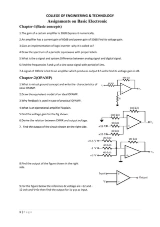
5.Find the voltage gain for the fig shown.
6.Derive the relation between CMRR and output voltage.
7. Find the output of the circuit shown on the right side.
8.Find the output of the figure shown in the right
side.
9.For the figure below the reference dc voltage are +12 and -
12 volt and V=0v then find the output for 1v p-p ac input.
2. 2 | P a g e
10.Find the values of the resistors so the the circuit provies o/p V0=2V1+V2-4V3 for the circuit shown
below.
11.For the circuit below if the gain is -10,then the value of R i
12.For the ckt determine the current through all resistors if input is 1v.
13.What are the advantage of instrumentation amplifier and also derive the o/p expression.
14.What is the o/p of an integrator and differentiator if a Step i/p is given.
3. 3 | P a g e
15.Find the gain for the circuit below.
16.The current i0 is if vi is 1.5v.
Chapter-3(Basics of semiconductor and PN junction diodes)
1.What is the cause and effect of the depletion layer in a pn junction diode?
2.Write down four applications of diode.
3.Compare the PIVs of a halfwave rectifier and full wave rectifier.
4.Explain why an inductor and a capacitor can act as filtering components.
5.Implement 2-i/p NAND gate by diode,transistor and resistors.
6. PN junction made up of which material (Si,Ge,GaAs) will have highest thermal stability and why ?
7. Give atleast two examples of semiconductors which are used for LED. Also express why?
8.What is a clipper circuit explain with an example?
9.Define mobility and conductivity of an intrinsicsemiconductor.
10.A diode has a reverse saturation current of 5µA at 250
c for a reverse voltage of 20v.Calculate the
reverse resistance.
11.An ideal diode acts like a bistable switch,justify.
12.Explain how diodes are useful in Clamping operation.Draw negative clamping circuit.Find the
relation between the time constant of the circuit and time period of the input signal.What should be
the full discharge time,in terms of the time constant of the circuit,for the capacitor you have used.
13.Explain the diode resistances and load line.
4. 4 | P a g e
14.Write the analytic equation for the current which describes both forward and reverse
characterstics of a diode.A silicon diode has a forward voltage drop of 1.2v for a forward dc current
of 100mA.It has a reverse current of 1µA for a reverse voltage of 10v.Claculate the bulk and reverse
resistance of the diode.Find the ac resistance at forward dc current of 25 mA.
15. Find the output.
16.Find the output.
17.Find the output.
18. Find the output.
5. 5 | P a g e
19.Why Si is preffered over Ge and what are the advantage of semiconductor.
20.Find the output.
21. Two junction diodes (identical) are connected as shown in fig. Find current through and voltage
across diode D1 and D2 .Given Is=0.2µA,ȵ=1,VT=25mV,supply voltage=15V
22. Derive all the parameters of rectifiers.
23. A full wave bridge rectifier with a 120V rms sinusoidal input has a load resistor of 1KΩ .
i)If silicon didodes are applied,what is the d.c voltage available at the load ?
ii)Determine the required PIV rating of each diode.
iii)Find maximum current through each diode during conduction.
iv)What is the power rating for each diode.
24.In the voltage regulator circuit find the power dissipation in the Zener diode.
Chapter-4 (Transistor and Its biasing)
1.Why NPN is preferred over PNP.
2.Why transistor is called so.
3.What is an amplifier.
6. 6 | P a g e
4.Why common collector configuration is also called emitter follower. And what is its use.
5.What are the needs of biasing? Write short note on biasing.
6.Define ICBO and ICEO. Derive an expression to find the relation between them.
7.Explain the operation of PNP transistor.
8.Explain base width modulation or Early effect.
9.Derive relation among all the current gains.
10.Draw the characteristics of CB and CE configuration.
11. What is the phase relation between all the three configurations.
12.For the circuit shown below Find IE and Rc.
13.Find IC,RC ? 14.Find Q point and VC?
14.Why CE is widely used.Explain.
15.Tabulate the i/p and o/p impendances of all the configurations.
16.Explain transistor as an Amplifier and Switch/Inverter.
7. 7 | P a g e
17.Given VCEQ and ICQ are 12V and 2A respectively when beta is 60 find the value of base and collector
resistors.
18.For the FIG a and b ,find the Q point. Given beta=100
19.Find the collector if minority current ,current gain and base current in CB configuration are 0.2µA
0.9 and 5µA respectively.
20.Derive the general expression of stability factor and also find the stability factor value of FIG a
and b of Question no.18.
21.Why fixed bias is called so and comment on its stability.
22.What is over drive factor.
23.How can we find in which region transistor is operating.
Prepared by: Mr.Soumya ranjan panda
Email-srpandaie@cet.edu.in