Embedded System Project Report on Bidirectional Visitor Counter
•Download as DOCX, PDF•
4 likes•1,564 views

This document appears to be an industrial training report submitted by Jitendra Dhaka to the National Institute of Technology in Hazratbal, Srinagar, India. The report details Dhaka's winter training on embedded systems conducted at TATA CMC Jaipur. It includes an acknowledgements section thanking various individuals and organizations for their support. It also includes a preface describing the benefits of industrial training for engineering students and an overview of the project Dhaka completed - a bidirectional visitor counter and home automation system.

Recommended
Recommended
More Related Content
What's hot
What's hot (20)
Viewers also liked
Viewers also liked (17)
Similar to Embedded System Project Report on Bidirectional Visitor Counter
Similar to Embedded System Project Report on Bidirectional Visitor Counter (20)
Recently uploaded
Recently uploaded (20)
Embedded System Project Report on Bidirectional Visitor Counter
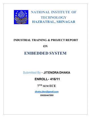
- 1. NATIONAL INSTITUTE OF TECHNOLOGY HAZRATBAL, SRINAGAR INDUSTRIAL TRAINING & PROJECT REPORT ON EMBEDDED SYSTEM Submitted By - JITENDRA DHAKA ENROLL- 416/11 7TH SEM ECE dhaka.jiten@gmail.com 09086447099
- 2. ACKNOWLEDGEMENT I have taken efforts in this training. However, it would not have been possible without the kind support and help of many individuals and organizations. I would like to extend my sincere thanks to all of them. I am highly indebted to TATA CMC JAIPUR for their guidance and constant supervision as well as for providing necessary information regarding the training & also for their support in completing the training. I would like to express my gratitude towards my parents & member of TATA CMC JAIPUR for their kind co-operation and encouragement which help me in completion of this training. I would like to express my special gratitude and thanks to industry persons for giving me such attention and time. My thanks and appreciations also go to my colleague in developing this training and people who have willingly helped me out with their abilities.
- 3. PREFACE Industrial Training is very important for engineering students. This training provides them opportunity to be familiar with the industrial / company environment. During this training they can show and can enhance their practical skills and gain practical knowledge and experience for future. This is best way through which the students can learn the latest technologies being used in the companies. I “JITENDRA KUMAR” have undergone through Winter Training on “Embedded system” from “TATA CMC JAIPUR”. This training helped me a lot in learning the technologies of this particular field. I have also done a project on “Bidirectional Visitor Counter & Home Automation” during the training under the guidance of “Mr. Vishwesh Kumar Sharma”. During the Project development I gained practical knowledge of the subject. Industrial Training & Project work were very challenging but as I proceeded things got easier. Practical Industrial Training was an interesting learning experience for me.
- 4. BIDIRECTIONAL VISITOR COUNTER & HOME AUTOMATION CONTENTS • INTRODUCTION • PROJECT OVERVIEW • PCB LAYOUT • CIRCUIT COMPONENTS • COMPONENTS DESCRIPTION • ABOUT MICROCONTROLLER • POWER SUPPLY • LCD • CIRCUIT DESIGN • OPERATION • SOFTWARE IN MCU 89S52 • ORIGINAL PCB LAYOUT • TRANSMITTER & RECEIVER CIRCUIT • APPLICATION & LIMITATIONS • PHOTOS OF BIDIRECTIONAL VISITOR COUNTER AND HOME AUTOMATION • CONCLUSION
- 5. INTRODUCTION The objective of this project is to make a controller based model to count number of persons visiting particular room and accordingly light up the room. Here we can use sensor and can know present number of persons. In today’s world, there is a continuous need for automatic appliances with the increase in standard of living, there is a sense of urgency for developing circuits that would ease the complexity of life. Also if at all one wants to know the number of people present in room so as not to have congestion. This circuit proves to be helpful.
- 6. PROJECT OVERVIEW This Project “Bi-directional Visitor Counter and Home Automation” using Microcontroller is a reliable circuit that takes over the task of controlling the room lights as well as counting number of persons/ visitors in the room very accurately. When somebody enters into the room then the counter is incremented by one and the light in the room will be switched ON and when any one leaves the room then the counter is decremented by one. The light will be only switched OFF until all the persons in the room go out. The total number of persons inside the room is also displayed on the seven segment displays. The microcontroller does the above job. It receives the signals from the sensors, and this signal is operated under the control of software which is stored in ROM. Microcontroller AT89S52 continuously monitor the Infrared Receivers, When any object pass through the IR Receiver’s then the IR Rays falling on the receiver are obstructed , this obstruction is sensed by the Microcontroller.
- 7. PCB LAYOUT BOTTOM SILK PCB LAYOUT
- 8. TOP SILK PCB LAYOUT
- 9. CIRCUIT COMPONENTS Here is the list of components and their corresponding values used in this circuit. 5 Resistor of 330 ohms 2 Variable Resistor of 20 Kohms 2 Variable Resistor of 50Kohms 2 Electrolytic Capacitor 4 Ceramic Capacitor 104 2 Ceramic Capacitor 33 pF 11.0592 MHz crystal Oscillator AT89S52 7 segment display 7805 7812 3 LED Reset Key 2 Relay ULN2803 Relay Driver IC LM324 IC IR LED IR Phototransistor
- 10. Components Description: LED Light emitting diodes (LEDs) are semiconductor light sources. The light emitted... Infrared LED An IR LED, also known as IR transmitter, is a special purpose LED that transmits infrared rays in the range of 760 nm wavelength. Transistor BC547 BC547 is an NPN bi-polar junction transistor. A transistor, stands for transfer of resistance, is commonly used to amplify current. A small current at its base controls a larger current...
- 11. Seven Segment Display A seven segment display is the most basic electronic display device that can display digits from 0-9. They find wide application in devices that display numeric information like digital clocks, radio, microwave ovens... AT89C51 Microcontroller AT89C51 is an 8-bit microcontroller and belongs to Atmel's 8051 family. ATMEL 89C51 has 4KB of Flash programmable and erasable read only memory (...
- 12. MICROCONTROLLER Various Type Of Microcontrollers: First microcontroller is “8031” It is Intel’s product. Neither a microprocessor nor a microcontroller. It is an 8-bit controller. Internally no ROM is provided i.e. code is outside the chip. Second microcontroller is “8051” It is a first complete 8-bit microcontroller. It is a name of a family. In which the instruction set, pin configuration, architecture are same, only memory storage capacity is different. Internally PROM (programmable read only memory) is provided so it called one time programmable (OTP). Third microcontroller is “AT89C51” It is ATMEL’s product. It is a similar to 8051 microcontroller i.e. having same instruction set, pin configuration, architecture. It is also 8-bit microcontroller. Its cost is only Rs10 more than 8051. It uses EPROM (erasable programmable read only memory) or FLASH memory. It is multiple time programmable (MTP) i.e. 1000 times. So it is better than 8051. In “AT89C51”, C‟ stands for CMOS technology used in the manufacturing of the I.C.
- 13. ATMEL89C52 Description: The AT89C52 is a low-power, high performance CMOS 8-it microcomputer with 8K bytes of Flash programmable and erasable read only memory (PEROM). The device is manufactured using Atmel’s high-density non-volatile memory technology and is compatible with the industry-standard 80C51 and 80C52 instruction set and pinout. The on-chip Flash allows the program memory to be reprogrammed in-system or by a conventional non-volatile memory programmer. By combining a versatile 8-bit CPU with Flash on a monolithic chip, the Atmel AT89C52 is a powerful microcomputer which provides a highly-flexible and cost-effective solution to many embedded control applications.
- 14. The ATMEL89C52 have a total of 40 pins that are dedicated for various functions such as I/O, RD, WR, address and interrupts. Out of 40 pins, a total of 32 pins are set aside for the four ports P0, P1, P2, and P3, where each port takes 8 pins. The rest of the pins are designated as VCC, GND, XTAL1, XTAL, RST, EA, and PSEN. All these pins except PSEN and ALE are used by all members of the 8051
- 15. Vcc: - Pin 40 provides supply voltage to the chip. The voltage source is +5 V. GND: - Pin 20 is the ground. XTAL1 and XTAL2: - The 8051 have an on-chip oscillator but requires external clock to run it. Most often a quartz crystal oscillator is connected to input XTAL1 (pin 19) and XTAL2 (pin 18). The quartz crystal oscillator connected to XTAL1 and XTAL2 also needs two capacitors of 30 pF value. One side of each capacitor is connected to the ground. RST:- Pin 9 is the reset pin. It is an input and is active high (normally low). Upon applying a high pulse to this pin, the microcontroller will reset and terminate all activities. This is
- 16. often referred to as a power –on reset. Activating a power- on reset will cause all values in the registers to be lost. Circuit Connection of Reset Pin PSEN:- This is an output pin. PSEN stands for “program store enable.” It is the read strobe to external program memory. When the microcontroller is executing from external memory, PSEN is activated twice each machine cycle. ALE:- ALE (Address latch enable) is an output pin and is active high. When connecting a microcontroller to external memory, potr 0 provides both address and data. In other words the microcontroller multiplexes address and data through port 0 to save pins. The ALE pin is used for de- multiplexing the address and data by connecting to the G pin of the 74LS373 chip.
- 17. I/O port pins and their functions:- The four ports P0, P1, P2, and P3 each use 8 pins, making them 8-bit ports. All the ports upon RESET are configured as output, ready to be used as output ports. To use any of these as input port, it must be programmed. Port 0:- Port 0 occupies a total of 8 pins (pins 32 to 39). It can be used for input or output. To use the pins of port 0 as both input and output ports, each pin must be connected externally to a 10K-ohm pull-up resistor. This is due to fact that port 0 is an open drain, unlike P1, P2 and P3. With external pull-up resistors connected upon reset, port 0 is configured as output port. In order to make port 0 an input, the port must be programmed by writing 1 to all the bits of it. Port 0 is also designated as AD0-AD7, allowing it to be used for both data and address. When connecting a microcontroller to an external memory, port 0 provides both address and data. The microcontroller multiplexes address and data through port 0 to save pins. ALE indicates if P0 has address or data. When ALE=0, it provides data D0-D7, but when ALE=1 it has address A0-A7. Therefore, ALE is used for de-multiplexing address and data with the help of latch 74LS373.
- 18. Port 1:- Port 1 occupies a total of 8 pins (pins 1 to 8). It can be used as input or output. In contrast to port 0, this port does not require pull-up resistors since it has already pull- up resistors internally. Upon reset, port 1 is configures as an output port. Similar to port 0, port 1 can be used as an input port by writing 1 to all its bits. Port 2:- Port 2 occupies a total of 8 pins (pins 21 to 28). It can be used as input or output. Just like P1, port 2 does not need any pull-up resistors since it has pull-up resistors internally. Upon reset port 2 is configured as output port. To make port 2 input, it must be programmed as such by writing 1s to it. Port 3:- Port 3 occupies a total of 8 pins (pins 10 to 17). It can be used as input or output. P3 does not need any pull- up resistors, the same as P1 and P2 did not. Although port 3 is configured as output port upon reset, this is not the way it is most commonly used. Port 3 has an additional function of providing some extremely important signals such as interrupts. Some of the alternate functions of P3 are listed below: P3.0 RXD (Serial input) P3.1 TXD (Serial output) P3.2 INT0 (External interrupt 0)
- 19. P3.3 INT1 (External interrupt 1) P3.4 T0 (Timer 0 external input) P3.5 T1 (Timer 1 external input) P3.6 WR (External memory write strobe) P3.7 RD (External memory read strobe) MEMORY SPACE ALLOCATION:- The 8051 has three very general types of memory. To effectively program the 8051 it is necessary to have a basic understanding of these memory types. The memory types are illustrated in the following graphic. They are: On-Chip Memory, External Code Memory, and External RAM. On chip ROM:- The 89C51 has a 4K bytes of on-chip ROM. This 4K bytes ROM memory has memory addresses of 0000 to 0FFFh. Program addresses higher than 0FFFh, which exceed the internal ROM capacity will cause the microcontroller to automatically fetch code bytes from external memory. Code bytes can also be fetched exclusively from an external memory, addresses 0000h to FFFFh, by connecting the external access pin to ground. The program counter doesn‟t care where the code is: the circuit designer decides whether the code is found totally in internal ROM,
- 20. totally in external ROM or in a combination of internal and external ROM. On chip RAM:- The 1289 bytes of RAM inside the 8051 are assigned addresses 00 to 7Fh. These 128 bytes can be divided into three different groups as follows: A total of 32 bytes from locations 00 to 1Fh are set aside for register banks and the stack. A total of 16 bytes from locations 20h to 2Fh are set aside for bit addressable read/write memory and instructions.
- 21. ROM & RAM Memory in The 8051 mc External Code Memory External Code Memory is code (or program) memory that resides off-chip. This is often in the form of an external EPROM. External RAM External RAM is RAM memory that resides off-chip. This is often in the form of standard static RAM or flash refers to any memory (Code, RAM, or other) that physically exists on the microcontroller itself. On-chip memory can be of several types, but we'll get into that shortly. Code Memory Code memory is the memory that holds the actual 8051 prk2ogram that is to be run. This memory is limited to 64K and comes in many shapes and sizes: Code memory may be found on-chip, either burned into the microcontroller as ROM or EPROM. Code may also be stored completely off-chip in an external ROM or, more commonly, an external EPROM. Flash RAM is also another popular method of storing a program. Various combinations of these memory types may also be used--that is to say, it is possible to have 4K of code memory on-chip and 64k of code memory offchip in an EPROM.
- 22. Registers In the CPU, registers are used to store information temporarily. That information could be a byte of data to be processed, or an address pointing to the data to be fetched. In the 8051 there is only one data type: 8 bits. With an 8- bit data type, any data larger than 8 bits has to be broken into 8-bit chunks before it is processed. The most commonly used registers of the 8051 are A (accumulator), B, R0, R1, R2, R3, R4, R5, R6, R7, DPTR (data pointer) and PC (program counter). All the above registers are 8-bit registers except DPTR and the program counter. The accumulator A is used for all arithmetic and logic instructions. Some 8051 8-bit registers R7 R6 R5 R4 R3 R2 R1 R0 B A
- 23. Some 8051 16-bit registers PC(program counter) DPL DPH DPTR PC Program Counter and Data Pointer The program counter is a 16- bit register and it points to the address of the next instruction to be executed. As the CPU fetches op-code from the program ROM, the program counter is incremented to point to the next instruction. Since the PC is 16 bit wide, it can access program addresses 0000 to FFFFH, a total of 64K bytes of code. However, not all the members of the 8051 have the entire 64K bytes of on-chip ROM installed. Flag bits and the PSW Register Like any other microprocessor, the 8051 have a flag register to indicate arithmetic conditions such as the carry bit. The flag register in the 8051 is called the program status word (PSW) register. The program status word (PSW) register is an 8-bit register. It is also referred as the flag register. Although the PSW register is 8-bit wide, only 6 bits of it are used by the
- 24. microcontroller. The two unused bits are user definable flags. Four of the flags are conditional flags, meaning they indicate some conditions that resulted after an instruction was executed. These four are CY (carry), AC (auxiliary carry), P (parity), and OV (overflow). The bits of the PSW register are shown below: CY PSW.7 Carry flag AC PSW.6 Auxiliary carry flag PSW.5 Available to the user for general purpose RS1 PSW.6 Register bank selector bit 1 RS0 PSW.3 Register bank selector bit 0 OV PSW.2 Overflow flag F0 PSW.1 User definable bit P PSW.0 Parity flag CY, the carry flag This flag is set whenever there is a carry out from the d7 bit. This flag bit is affected after an 8-bit addition or subtraction. It can also be set to 1 or 0 directly by an instruction such as “SETB C” and “CLR C” where “SETB C” stands for set bit carry and “CLR C” for clear carry.
- 25. AC, the auxiliary carry flag If there is carry from D3 to D4 during an ADD or SUB operation, this bit is set: otherwise cleared. This flag is used by instructions that perform BCD arithmetic. P, the parity flag The parity flag reflects the number of 1s in the accumulator register only. If the register A contains an odd number of 1s, then P=1.Therefore, P=0 if A has an even number of 1s. OV, the overflow flag This flag is set whenever the result of a signed number operation is too large, causing the high order bit to overflow into the sign bit. In general the carry flags is used to detect errors in unsigned arithmetic operations POWER SUPPLY UNIT (+5V) Power supplies are designed to convert high voltage AC mains electricity to a suitable low voltage supply for electronic circuits and other devices. A power supply can by broken down into a series of blocks, each of which performs a particular function.
- 26. Each of the block has its own function as described below Transformer – steps down high voltage AC mains to low voltage AC. Rectifier – converts AC to DC, but the DC output is varying. Smoothing – smooths the DC from varying greatly to a small ripple. Regulator – eliminates ripple by setting DC output to a fixed voltage.
- 27. LIQUID CRYSTAL DISPLAYS (LCD) Liquid crystal displays (LCD) are widely used in recent years as compares to LEDs. This is due to the declining prices of LCD, the ability to display numbers, characters and graphics, incorporation of a refreshing controller into the LCD, their by relieving the CPU of the task of refreshing the LCD and also the ease of programming for characters and graphics. HD 44780 based LCDs are most commonly used. LCD pin description: The LCD discuss in this section has the most common connector used for the Hitachi 44780 based LCD is 14 pins in a row and modes of operation and how to program and interface with microcontroller is describes in this section.
- 28. VCC,VSS,VEE: The voltage VCC and VSS provided by +5V and ground respectively while VEE is used for controlling LCD contrast. Variable voltage between Ground and Vcc is used to specify the contrast (or "darkness") of the characters on the LCD screen. RS (register select): There are two important registers inside the LCD. The RS pin is used for their selection as follows. If RS=0, the instruction command code register is selected, then allowing to user to send a command such as clear display, cursor at home etc.. If RS=1, the data register is selected, allowing the user to send data to be displayed on the LCD. R/W (read/write): The R/W (read/write) input allowing the user to write information from it. R/W=1, when it read and R/W=0, when it writing. EN (enable): The enable pin is used by the LCD to latch information presented to its data pins. When data is supplied to data pins,
- 29. a high power, a high-to-low pulse must be applied to this pin in order to for the LCD to latch in the data presented at the data pins. D0-D7 (data lines): The 8-bit data pins, D0-D7, are used to send information to the LCD or read the contents of the LCD‟s internal registers. To displays the letters and numbers, we send ASCII codes for the letters A-Z, a-z, and numbers 0-9 to these pins while making RS =1. There are also command codes that can be sent to clear the display or force the cursor to the home position or blink the cursor. We also use RS =0 to check the busy flag bit to see if the LCD is ready to receive the information. The busy flag is D7 and can be read when R/W =1 and RS =0, as follows: if R/W =1 and RS =0, when D7 =1(busy flag =1), the LCD is busy taking care of internal operations and will not accept any information. When D7 =0, the LCD is ready to receive new information.
- 30. INTERFACING OF LCD WITH MICROCONTROLLER: An intelligent LCD has two lines with 20 characters each line. The display contains two internal byte wide registers, one for commands and second for characters to be displayed. It also contains a user programmed RAM area that can be programmed to generate any desired character that can be formed using a dot matrix. To distinguish between these two data areas, the hex command byte 80 will be used to signify that the display RAM address 00h is chosen. From diagram Port 1 of microcontroller is used for 8 bit data display on the LCD. Data lines of the LCD Pin no.7 to pin no 14 are connected to the port 1 of the microcontroller. The control pin no.4 register select is connected to P3.5, pin no.5 of LCD for Read/write is connected to P3.6 and the enable pin (6) is connected to microcontroller
- 32. Circuit Design The heart of the circuit design lies in designing the microcontroller interface. Here we use the microcontroller AT89S52. The microcontroller AT89S52 is interfaced to the IR sensor pairs at two ports pins – P1.0 and P1.1 respectively. The 7 segment display is interfaced to the microcontroller at port P2. Another important aspect of the design involves designing the oscillator circuit and the reset circuit. The oscillator circuit is designed by selecting an 11.0592MHz quartz crystal and two ceramic capacitors each 33pF. The reset circuit is designed by selecting an electrolyte capacitor of 10uF to ensure a reset pulse width of 100ms and reset pin voltage drop of 1.2V. The sensor circuit is designed by selecting appropriate value of resistors for both the LED and the phototransistor.
- 33. Operation: When the system is powered, the compiler initially initializes the stack pointer and all other variables. It then scans the input ports (PortP1.0 first). In the meantime, when there is no interruption between the IR LED and the phototransistor of the first sensor pair, the output of the phototransistor is always at low voltage. In other words port P1.0 is at logic low level. Now when a transition takes place, i.e. a logic high level is received at port P1.0, the compiler sees this as an interruption to sense the passage of a person or an object between the IR LED and the phototransistor. As per the program, the count value is increased and this value is displayed on the Counter. Now the compiler starts scanning the other input pin-P1.1. Similar to the first sensor pair, for this sensor pair also the phototransistor conducts in absence of any interruption and P1.1 is at logic low level. In case of an interruption, the pin P1.1 goes high and this interruption is perceived by decreasing the value of cou;8nt. The program ensures that the scanning of both the port pins is done at certain delays so as to avoid confusion of reading. For instance port P1.0 is scanned for two or three interruptions so as to ensure the count value is above 1 or 2.
- 34. SOFTWARE Keil an ARM Company makes C compilers, macro assemblers, real-time kernels, debuggers, simulators, integrated environments, evaluation boards, and emulators for ARM7/ARM9/Cortex-M3, XC16x/C16x/ST10, 251, and 8051 MCU families. Compilers are programs used to convert a High Level Language to object code. Desktop compilers produce an output object code for the underlying microprocessor, but not for other microprocessors PROGRAM #include<reg51.h> sbit s1=P1^0;sbit s2=P1^1; sbit HB=P3^0;sbit LB=P3^1; sbit fan1=P3^7;sbit fan2=P3^6; A[;810]={0xC0,0xF9,0xA4,0x30,0x19,0x12,0x02,0xF8,0x00,0x10}; void show(int,int); void main()
- 35. {int a=0,b=0; while(1) {if(a==10) {b++;a=0;} if(a==-1) {b--;a=9;} if(b==-1 || b==10) {b=0;a=0;} while(s1==1 && s2==1) {show(a,b); if(a<=1) {fan1=1;fan2=1;} if(a==2) {fan1=0;fan2=1;} if(a>=3) {fan1=0;fan2=0;}} if(s1==0 && s2==1) {while(s1==0 && s2==1)show(a,b); while(s1==1 && s2==1)show(a,b); if(s1==1 && s2==0)
- 36. {while(s1==1 && s2==0)show(a,b); a++;}} if(s1==1 && s2==0) {while(s1==1&&s2==0)show(a,b); while(s1==1 && s2==1)show(a,b); if(s1==0 && s2==1) {while(s1==0 && s2==1)show(a,b); a--;}} }} void show(int a,int b) { unsigned int i; HB=1;LB=0;P2=A[b]; //1st seg. for(i=0;i<0x04F;2F;i++); //delay HB=0;LB=1;P2=A[a]; //2nd seg. for(i=0;i<0x04FF;i++); //delay }
- 38. Original PCB Layout for Circuit
- 39. FINAL CIRCUIT
- 40. Applications: 1. This circuit can be used domestically to get an indication of number of persons entering a party 2. It can be used at official meetings. 3. It can be used at homes and other places to keep a check on the number of persons entering a secured place. 4. It can also be used as home automation system to ensure energy saving by switching on the loads and fans only when needed. Limitations: 1. It is a theoretical circuit and may require few changes in practical implementation. 2. It is a low range circuit and cannot be implemented at large areas. 3. With frequent change in the count value, after a certain time the output may look confusing.
- 41. Picture of functional Bidirectional Visitor Counter
- 44. CONCLUSION The training was really very good. I have learned on how to emphasise on important thing which we miss in our daily life. We keep on learning complex thing while ignoring basics butimportantaspect that’swhy we don’t understand everything in good way. From CMC Academy and especially Mr. Vishwesh Sir I have learnt thebasics which I hopewill be very beneficial for me in coming future. Once again I thank everybody of CMC Family for such a good training program.
- 45. BIBILOGRAPHY home-automation.org/ “The 8051 Microcontroller and Embedded systems” by Muhammad Ali Mazidi and Janice Gillispie Mazidi , Pearson Education. smart-home-automation-guide.com www.atmel.com/atmel/acrobat/doc0265.pdf ATMEL 89S51 Data Sheets. www.atmel.com