Orlando’s Arnold Palmer Hospital Layout Strategy-1.pptx
Transmission and reception of data through usb using
1. IJRET: International Journal of Research in Engineering and Technology eISSN: 2319-1163 | pISSN: 2321-7308
_______________________________________________________________________________________
Volume: 03 Special Issue: 01 | NC-WiCOMET-2014 | Mar-2014, Available @ http://www.ijret.org 110
TRANSMISSION AND RECEPTION OF DATA THROUGH USB USING
FPGA
Dinah Ann Varughese1
1
Assistant Professor, ECE Department, St. Thomas College Of Engineering & Technology, Kerala, India.
Abstract
The Universal Serial Bus (USB) replaces different communication interfaces with high speed of data transfer rate. To enable high
speed data transfer, I proposed FPGA based controller for the transmission and reception of data. This FPGA based controller
should be designed in such a way that it must be able to detect and communicate with USB port and must be able to transmit large
amounts of data between a personal computer and a memory storage device.
----------------------------------------------------------------------***----------------------------------------------------------------------
1. INTRODUCTION
The universal serial bus (USB) is an I/O interface standard. It
is a connection between a host computer and a number of
peripheral devices. And it was originally created to replace a
wide range of slow and different buses-the parallel and the
serial. USB has grown beyond these slow connections and
supports almost every type of device that can be connected to
a PC. Features of USB are high-bandwidth, easiness of use,
hotplug capability. Besides, the driver is one of the important
technological aspects in the development of USB device,
which directly affects the system performance of entire
equipment, so the writing of driver is necessary inorder to
realize the software’s access to hardware.
In this project paper it is proposed to implement an USB
controller which provides data transfer between an USB
device and PC. It is implemented using FPGA integrated
circuit- Xilinx Spartan 3E.
2. SYSTEM ARCHITECTURE
2.1 Architecture Overview
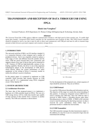
The basic idea of this proposed project is to implement a
hardware of a USB controller based on FPGA. The core of a
USB storage device will be a bulk data transfer type capable
of large amount of data transfer from a memory to another
memory. The USB core schematic is shown below:
For the development of this proposed core, certain sequence of
steps should be carried out. They are as follows:
2.1.1 USB Protocol
It is used for USB protocol decoding and information read out.
The objective of this stage is to assure the correct decoding of
data packets. A transceiver integrated circuit USB1T11A is
used to interface the USB lines. Once the USB bus data is
received in NRZI format, a decoding process takes place.
Decoding process is done in VHDL. A NRZI to RZ converter
circuit is used for detecting the data being received. As data is
received the cyclic redundancy check (CRC) logic is
performed inorder to validate the received data.
2.1.2 USB Transmitter
The USB transmitter manages the data transmission output i.e.
the addition of a zero bit in case six consecutive logic ones are
transmitted (bit stuffing).
2. IJRET: International Journal of Research in Engineering and Technology eISSN: 2319-1163 | pISSN: 2321-7308
_______________________________________________________________________________________
Volume: 03 Special Issue: 01 | NC-WiCOMET-2014 | Mar-2014, Available @ http://www.ijret.org 111
2.1.3 External Interface
External interface can be made through a PicoBlaze
microcontroller.
2.2 Objective
The main objective of this paper is to implement a FPGA
based core in order to receive and transmit the data from a
host device (PC) to USB device or vice-versa.
3. SYSTEM DESIGN REQUIREMENTS
3.1 Functional Requirement Specification
• Since this project deals with the data transferring
between two memory storage devices using bulk
transfer type, the input and output of the proposed core
must be data in the form of packets whose size cannot
be exceed than the allowable size which is 512 bytes.
• Shift register is used for the serial to parallel logic. Out
of the four shift registers, SIPO shift register is taken.
• Clock to the core is provided by the internal clock of
the hardware tool used.
3.2. Hardware and Software Realization
The proposed design is planned to be described using
VHDL(VHSIC Hardware Description Language) and
simulated by ModelSim and can be implemented on Xilinx
Spartan 3E FPGA(Field Programmable Gate Array).
3.3 Hardware Implementation
Fig 2 Hardware Model
This represents the actual transfer of data across the USB
cable between the host system (PC) and the USB devices. The
host side consists of the USB host controller, while the USB
side contains the USB interface within the device. All
communication on USB originates at the host under software
control. The host hardware contains the USB host controller,
which initiates transactions over the USB system.
4. IMPLEMENTATION METHODOLOGY &
SIMULATION
4.1 Introduction
This chapter describes the implementation of the proposed
controller. It consists of transmitter section, receiver section
and a controller section. The controller section controls the
transmission and reception of the data. The controller section
does the NRZI encoding, bit stuffing for the transmitter
section only when the control transmits signal is high. The
controller section does the NRZI decoding, bit unstuffing,
CRC generation, CRC checking for the receiver section only
when the control receive signal is high. The controller section
extracts the required data from a continuous serial data stream
and stores it in a buffer which is placed in a receiver section.
The proposed core is successfully simulated in ModelSim.
4.2 Implementation of Receiver Section
4.2.1 NRZI Decoder
The USB devices employ NRZI data encoding for
transmission of data. In NRZI encoding, logic 1 is represented
by no change in level and logic 0 is represented by a change in
level. So there is need for conversion of NRZI to RZ.
4.2.2 Bit Unstuffer
In order to ensure adequate signal transitions, bit stuffing is
employed by the transmitting device when sending a packet on
USB. A zero is inserted after every six consecutive ones in the
data stream before the data is NRZI encoded, to force a
transition in the NRZI data stream.
4.2.3 Byte Counter
It counts the number of bit received which helps to identify the
amount of data.
4.2.4 CRC Checker
The Cyclic Redundancy Checksums (CRC) is used to protect
all non-PID fields in token and data packets from errors.
4.3 Implementation of Transmitter Section
4.3.1 NRZI Encoder
The USB devices employ NRZI data encoding for
transmission of data packet. In NRZI encoding, logic 1 is
represented by no change in level and logic 0 is represented by
a change in level.
4.3.2 Bit Stuffer
It is employed by the transmitting device when sending a
packet on USB. A zero is inserted after every six consecutive
ones in the data stream before the data is NRZI encoded, to
3. IJRET: International Journal of Research in Engineering and Technology eISSN: 2319-1163 | pISSN: 2321-7308
_______________________________________________________________________________________
Volume: 03 Special Issue: 01 | NC-WiCOMET-2014 | Mar-2014, Available @ http://www.ijret.org 112
force a transition in the NRZI data stream. This bit stuffer
adds the stuff bit if six consecutive ones are found.
4.3.3 Serial Shifter
It is a serial shift register. It converts the parallel data to serial
data stream.
4.3.4 Byte Counter
This byte counter counts the number of bytes that are
transmitted.
4.4 Functional Requirements
The proposed core needs software and hardware requirements.
The core is simulated using ModelSim and written in VHDL
code. The core is implemented on Xilinx FPGA.
4.5 Simulation Results
4.5.1 Transmitter Section
Fig 3. Simulation Results of Transmitter Section
4. IJRET: International Journal of Research in Engineering and Technology eISSN: 2319-1163 | pISSN: 2321-7308
_______________________________________________________________________________________
Volume: 03 Special Issue: 01 | NC-WiCOMET-2014 | Mar-2014, Available @ http://www.ijret.org 113
4.5.2 Receiver Section
5. IJRET: International Journal of Research in Engineering and Technology eISSN: 2319-1163 | pISSN: 2321-7308
_______________________________________________________________________________________
Volume: 03 Special Issue: 01 | NC-WiCOMET-2014 | Mar-2014, Available @ http://www.ijret.org 114
Fig 4 Simulation Results of Receiver Section
4.6 Design Summary
Table 1. Device Utilization Summary
5. CONCLUSIONS
This paper is an approach for the implementation of the USB
device core on FPGA. The proposed core can also be used in a
memory storage device using bulk data transfer type. The
currently available memory storage device contains a flash
memory and a controller part. It requires both hardware and
software. Hence the memory for a given specification of a
storage device is less compared to the proposed core. Since the
proposed core is implemented using hardware, more memory
is available and increases the speed of the data transfer.
To conclude the proposed core has a number of important
advantages as the small space it requires from the FPGA
circuit, low cost and the advantage of using internal resources
included in the selected FPGA, as Pico Blaze microcontroller,
included in Xilinx Spartan III series and that is part of the
USB core.
REFERENCES
[1]. Universal Serial Bus Specification. September 1998.
www.usb.org
[2]. USB IT1 1A Universal Serial Bus Transceiver data Sheet.
Fairchild Corp. March 2005.
[3]. Fairchild Corp. Application Note 5015 - USB Transceiver
and Specification Compliance.
[4]. Penny Orwick - Guy Smith. "Developing Drivers with the
Windows Driver Foundation." Microsoft Press. April 2007.
ISBN-13: 978-0735623743
[5]. Walter Oney. "Programming the Microsoft Windows
Driver Model", Second Edition. Microsoft Press, December
2002. ISBN-13: 978-0735618039
[6]. Don Anderson, "Universal Serial Bus System
Architecture", 2nd. edition, MindShare Inc. 2001. ISBN-13:
978-0201309751
[7]. Jan Axelson, “USB Complete-The Developer’s Guide”,
4th.edition, Lakeview Research LLC, 5310 Chinook Ln.,
Madison WI 53704. ISBN-13 978-1-931448-08-6
BIOGRAPHIE:
Dinah Ann Varughese was born in
Chengannur,India in 1987.She received the
BTech degree in Electronics and
communication Engineering from Mahatma
Gandhi University, India in 2009,and the
MTech in VLSI and Embedded Systems from
Cochin University of Science and Technology, Cochin in
2011. In 2011, she joined the department of Electronics and
Communication Engineering, St.Thomas College of
Engineering and Technology Chengannur as Assistant
Professor. Her research interest is centered mainly in
designing of controller part using FPGA, Microcontroller
based system design.