PERFORMANCE EVALUATION OF LOW POWER CARRY SAVE ADDER FOR VLSI APPLICATIONS
Fd3110361040
1. Dakupati.Ravi Sankar, Shaik Ashraf Ali / International Journal of Engineering Research and
Applications (IJERA) ISSN: 2248-9622 www.ijera.com
Vol. 3, Issue 1, January -February 2013, pp.1036-1040
Design of Wallace Tree Multiplier by Sklansky Adder.
Dakupati.Ravi Sankar1, Shaik Ashraf Ali2.
NRI Institute of Technology, Pothavarrapadu, Agiripalli (M),
Vijayawada –522212, Andhra Pradesh, India
Abstract—
Power consumption has become a critical array for computing the partial products, a carry save
concern in today’s VLSI system design. The adder for adding the partial products so obtained and
growing market for fast floating-point co- a carry propagate adder in the final stage of addition.
processors, digital signal processing chips, and In the proposed architecture, partial product reduction
graphics processors has created a demand for is accomplished by the use of 4:2, 5:2 compressor
high speed, area-efficient multipliers .A Wallace structures and the final stage of addition is performed
tree multiplier is an improved version of tree by a Sklansky adder.
based multiplier architecture. It uses carry save
addition algorithm to reduce the latency. This II. PARTIAL PRODUCT REDUCTION
paper aims at additional reduction of latency and The multiplier architecture comprises of a
power consumption of the Wallace tree multiplier. partial product generation stage, partial product
This is accomplished by the use of 3:2,4:2, 5:2 reduction stage and the final addition stage. In the
compressors and by the use divide and conquer proposed architecture, multi bit compressors are used
tree adder (Sklansky adder). The result shows for realizing the reduction in the number of partial
that the proposed architecture is 3.46% decrease product addition stages. The combined factors of low
in delay than the conventional CMOS power, low transistor count and minimum delay
architecture, along with 11.6% of reduced power makes the 3:2,4:2 and 5:2 compressors, the
consumption realization at 50MHz. The appropriate choice. In these compressors, the outputs
simulations have been carried out using the Xilinx generated at each stage are efficiently used by
ISE tool. replacing the XOR blocks with multiplexer blocks
.The select bits to the multiplexers are available much
Keywords- Wallace tree, Sklansky adder, ahead of the inputs so that the critical path delay is
Compressors, adder, multiplier. minimized.
I. INTRODUCTION
The multiplier is one of the key hardware
blocks in most of the digital and high performance
systems such as digital signal processors and
microprocessors. With the recent advances in
technology, many researchers have worked on
the design of increasingly more efficient multipliers.
They aim at offering higher speed and lower power
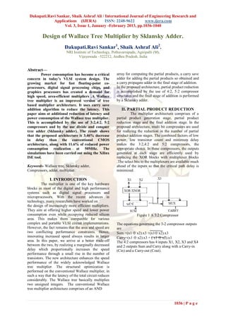
consumption even while occupying reduced silicon Figure 1 A 3:2 Compressor
area. This makes them compatible for various
complex and portable VLSI circuit implementations. The equations governing the 3-2 compressor outputs
However, the fact remains that the area and speed are are
two conflicting performance constraints. Hence, Sum =(x1 x2).x3 +(x1 x2).x3
innovating increased speed always results in larger Carry=(x1 x2).x3 + ( x1 x2).x1
area. In this paper, we arrive at a better trade-off The 4:2 compressors has 4 inputs X1, X2, X3 and X4
between the two, by realizing a marginally decreased and 2 outputs Sum and Carry along with a Carry-in
delay which proportionally increases the speed (Cin) and a Carry-out (Cout).
performance through a small rise in the number of
transistors. The new architecture enhances the speed
performance of the widely acknowledged Wallace
tree multiplier. The structural optimization is
performed on the conventional Wallace multiplier, in
such a way that the latency of the total circuit reduces
considerably. The Wallace tree basically multiplies
two unsigned integers. The conventional Wallace
tree multiplier architecture comprises of an AND
1036 | P a g e
2. Dakupati.Ravi Sankar, Shaik Ashraf Ali / International Journal of Engineering Research and
Applications (IJERA) ISSN: 2248-9622 www.ijera.com
Vol. 3, Issue 1, January -February 2013, pp.1036-1040
Figure 4 A 5:2 Compressor
Table I presents the latency comparison of 4:2 and
5:2 compressors with conventional CMOS structures.
Figure 2 A 4:2 Compressor (DPL logic)
Figure 3 A 4:2 Compressor
Figure 4. Carry generation module (C GEN)
Double pass transistor logic (DPL) implementation of
the gate logic structure shown above has been shown TABLE I. LATENCY COMPARISON OF
to exhibit lower power consumption and higher speed COMPRESSORS WITH CONVENTIONAL
performance compared to earlier designs due to its STRUCTURES
reduction of the internal load capacitances in the
critical path. The use of transmission gate multiplexer Circuit Structure Latency Comparison
in the construction of compressors further reduces the 4:2 5:2
number of transistors to 8 which would have been 12 Conventional CMOS 4 6
in the case of conventional CMOS multiplexer. On Compressor 3 4
the other hand, the use of a 4:2 compressor reduces
the latency to 3. Hence, two full adders can be The logic equation for the 5:2 compressors can be
replaced by a single 4:2 compressor. The equations written as
governing the outputs of the 4:2 compressor
Sum=x1 x2 x3 x4 x5 Cin1Cin2
architecture is shown below.
Cout1=(x1+x2). x3+x1.x2
Cout2=(x4 x5).Cin1+(x4 x5).x4
Sum=(x1 x2). (x3 x4)+ (x1 x2). (x3 x4).
Carry=((x1 x2 x3) (x4 x5 Cin1)).Cin2+
Cin+ (x1 x2). x3 x4+ (x1 x2). (x3 x4). Cin
(( x1 x2 x3 ) (x4 x5 Cin1)).
Cout=(x1 x2). x3+(x1 x2).x1
(x1 x2 x3)
Carry=(x1 x2 x3 x4.Cin1)+
III. TREE ADDERS FOR CARRY PROPAGATION
( x1 x2 x3 x4).x4 The final stage in the Wallace tree multiplier for
Similarly, when three full adders are used for the addition of partial products can be further reduced by
computation of sum and the resulting carry bit, it the use of tree adders. Binary addition is one of the
incurs a latency of 6. However, the use of a 5:2 most primitive and most commonly used applications
compressor in its place reduces the latency to 4. in computer arithmetic. The requirements of the
Hence, in this modified structure, a 5:2 compressor adder are that it should be primarily fast and
replaces three full adders. secondarily efficient in terms of power consumption
and chip area. Parallel-prefix adders are suitable for
VLSI implementation since they rely on the use of
simple cells and maintain regular connections
between them. Here, the Sklansky type of tree adder
is preferred due to its lower power consumption than
that incurred by other tree adder structures.
1037 | P a g e
3. Dakupati.Ravi Sankar, Shaik Ashraf Ali / International Journal of Engineering Research and
Applications (IJERA) ISSN: 2248-9622 www.ijera.com
Vol. 3, Issue 1, January -February 2013, pp.1036-1040
Furthermore, the latency of Sklansky adder is operations is required. Using the carry save adder,
reduced to 6, which is less than that realized by Brent three partial product terms can be added at a time to
Kung, Han Carlson and Ladner-Fischer tree adder form the carry and sum. The sum signal is used by
circuit. the full adder of next level. The carry signal is used
by the adder involved in the generation of the next
output bit, with a resulting overall delay proportional
to log3/2n, for n number of rows. In the first and
second stages of the Wallace structure, the partial
products do not depend upon any other values other
than the inputs obtained from the AND array.
However, for the immediate higher stages, the final
value (PP3) depends on the carry out value of
previous stage. This operation is repeated for the
consecutive stages. Hence, the major cause of delay
Figure 5. Skalansky Tree adder structure
is the propagation of the carry out from the previous
stage to the next stage. In conventional Wallace tree
structure, the total number of stages in the critical
path sums up to 13. Each full adder accounts for a
latency of 2. Therefore, the total latency of the given
structure when calculated is 26. The latency count
gets added by one, when considering the AND array,
thus resulting in a total latency.
Figure 6. Black Cell.
Figure 7. Grey Cell
In the Sklansky adder, the binary trees of cells first
Generate all the carry input bits simultaneously. This Figure 8 Schematic of Wallace tree multiplier
architecture follows a regular pattern. The Sklansky depicting critical path
adder ultimately reduces the delay to log2N by B. Proposed architecture
computing intermediate prefixes along with the large Our proposed architecture aims to reduce the
group prefixes. Here, N represents the number of bits. overall latency. This leads to increased speed and
This also results in an increased number of fan-outs reduced power consumption. The design makes use
at each level. In Fig. 5, the black squares correspond of compressors in place of full adders, and the final
to AND-OR-AND logic and grey squares correspond carry propagate stage is replaced by a Sklansky tree
to AND-OR logic. The triangular box represents adder. Figure 9 depicts the first stage consisting of a
buffers. full adder. In the second stage, two full adders have
been grouped and implemented using a4:2
IV. CONVENTIONAL AND PROPOSED compressors. Similarly, the third stage consists of a
WALLACE TREE MULTIPLIERS 5:2 compressor, which is a combination of 3 full
A. Conventional Wallace tree multiplier adders and so on. In this manner, the individual full
In the conventional 8 bit Wallace tree adder blocks in the original structure are grouped and
multiplier design, more number of addition
1038 | P a g e
4. Dakupati.Ravi Sankar, Shaik Ashraf Ali / International Journal of Engineering Research and
Applications (IJERA) ISSN: 2248-9622 www.ijera.com
Vol. 3, Issue 1, January -February 2013, pp.1036-1040
implemented using compressors. The number of
interconnections is taken care of, since they play a
vital role in the flow of carry from one stage to the
next in the tree. From Fig. 9, we can see that the
longest delay path of our design is the one consisting
of two 5:2 compressors, which produces a reduced
latency of 8 (four per compressor) only. The use of
the Sklansky adder in the structure further results in a
reduced latency of 6 with a latency of 1 for the AND
array. Hence, this novel structure brings down the
overall latency count to 15. Thus, a significant
latency reduction of 44.4% than the conventional
counterpart is realized. The symbolic arrangement of
the proposed structure is depicted in Fig. 10 for
Figure 10 Proposed Wallace tree multiplier
elaboration.
Comparison, the latency comparison and total
memory usage are shown in Table II. The latency
defines the number of total phases required to
compute the output and is found to be 44.4% less
than the latency of the conventional Wallace tree
multiplier.
Table III shows the delay comparison in nano
seconds.
Table IV shows the power consumption of the
conventional and proposed multipliers operated at
50MHz for various supply voltage levels.
Table II
Circuit Structure Wallace Tree Multiplier
No of Latency Total
Devices Memory
Usage(KB)
Conventional 2748 27 67840
Proposed 2998 15 54844
Table III
Circuit Structure Delay(ns)
Figure 9 Schematic of Proposed Wallace tree
multiplier Logic Route Total
Level Delay
Conventional 14.346 8.141 22.487
Proposed 13.580 8.131 21.711
V RESULT AND DISCUSSION
In this section, the proposed and the
conventional architectures have been compared. The Table IV
transistor count Circuit Structure Power in mW at frequency 50MHz
1.14V 1.18V 1.20V 1.24V
Conventional 167.87 171.73 173.75 177.98
Proposed 147.66 151.47 153.47 157.65
VI CONCLUSION
In this paper, the implementation and
analysis of a novel Wallace tree architecture is
proposed. The latency of existing Wallace tree
multiplier which is found to be 27 has been reduced
to 15.The comparison result also shows that a
1039 | P a g e
5. Dakupati.Ravi Sankar, Shaik Ashraf Ali / International Journal of Engineering Research and
Applications (IJERA) ISSN: 2248-9622 www.ijera.com
Vol. 3, Issue 1, January -February 2013, pp.1036-1040
significant reduction of power is achieved. At an
operating frequency of 50 MHz at 1.2V, the power is
found to be 153.47mW. It is a realization of 11.6% of
power reduction than the conventional Wallace tree
multiplier. At 1.14V,the power consumed is found to
be 147.66mW, which is a 12.03% reduction of that
obtained from the existing architecture. The results
prove that the proposed architecture is more efficient
than the conventional one in terms of
Power consumption and latency.
REFERENCES
[1] A. P. Chandrakasan and R. W. Brodersen, Low
Power Digital CMOS Design. Norwell.
MA:Kluwer.
[2] C. H. Chang, J. Gu, M. Zhang, “Ultra low-
voltage low power CMOS 4-2 and 5-2
compressorsfor fast arithmetic circuits” IEEE
Transactions on Circuits and Systems .
[3] H. Neil. Weste and Kamran Eshraghian,
“Principles of CMOS VLSI design-A Systems
Perspective,” Pearson Edition Pvt Ltd. 3rd
edition, 2005.
[4] J. M. Rabaey, A. Chandrakasan , and B.
Nikolic, Digital“IntegratedCircuits(Adesign
perspective)”.
[5] List I. Abdellatif, E. Mohamed, “Low-Power
Digital VLSI Design,Circuits and Systems,”
Kluwer Academic Publishers.
[6] Milos Ercegovac, Tomas Lang, "Digital
Arithmetic",Morgan Kaufman,.
[7] R. Zimmermann and W.Fichtner, “Low-power
logic styles: CMOS versus pass-transistor
logic,” IEEE J. Solid- State Circuits.
[8] S. F. Hsiao, M. R. Jiang, and J. S. Yeh ,
“Design of high speed low-power 3-2 counter
and 4-2 compressor for fast multipliers,”.
[9] Z. Wang, G. A. Jullien, and W. C. Miller, “A
new design technique for column compression
multipliers,”.
.
.
1040 | P a g e