1. LF153
LF253 - LF353
®
WIDE BANDWIDTH
DUAL J-FET OPERATIONAL AMPLIFIERS
.
.
.
.
.
.
.
.
LOW POWER CONSUMPTION
WIDE COMMON-MODE (UP TO VCC+) AND
DIFFERENTIAL VOLTAGE RANGE
LOW INPUT BIAS AND OFFSET CURRENT
OUTPUT SHORT-CIRCUIT PROTECTION
HIGH INPUT IMPEDANCE J–FET INPUT
STAGE
INTERNAL FREQUENCY COMPENSATION
LATCH UP FREE OPERATION
HIGH SLEW RATE : 16V/µs (typ)
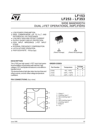
N
DIP8
(Plastic Package)
D
SO8
(Plastic Micropackage)
DESCRIPTION
The LF353 are high speed J–FET input dual operational amplifiers incorporating well matched, high
voltageJ–FET andbipolartransistorsin a monolithicintegrated circuit.
The devicesfeaturehigh slew rates, low input bias and
offset currents, and low offset voltage temperature
coefficient.
ORDER CODES
Part Number
Temperature
Package
N
D
LF353
0 C, +70 C
•
•
LF253
–40oC, +105oC
•
•
LF153
–55 C, +125 C
•
•
o
o
o
o
PIN CONNECTIONS (top view)
1
8
2
-
3
+
4
June 1998
7
-
6
+
1
2
3
4
5
6
7
8
- Output 1
- Inverting input 1
- Non-inverting input 1
- VCC- Non-inverting input 2
- Inverting input 2
-Output 2
+
- VCC
5
1/9
2. LF153 - LF253 - LF353
SCHEMATIC DIAGRAM (each amplifier)
VCC
input
Non-inverting
input
Inverting
100 Ω
200 Ω
Output
100 Ω
30k
8.2k
1.3 k
35k
1.3k
35k
100 Ω
VCC
Offs e t Null1
Offse t Null2
ABSOLUTE MAXIMUM RATINGS
Symbol
Parameter
Value
Unit
Supply Voltage - (note 1)
±18
V
Vi
Input Voltage - (note 3)
±15
V
Vid
Differential Input Voltage - (note 2)
±30
V
Ptot
Power Dissipation
680
mW
VCC
Output Short-circuit Duration - (note 4)
Toper
Operating Free Air Temperature Range
Tstg
Storage Temperature Range
Notes :
2/9
Infinite
LF353
LF253
LF153
0 to 70
–40 to 105
–55 to 125
o
–65 to 150
o
C
C
1. All voltage values, except differential voltage, are with respect to the zero reference level (ground) of the supply voltages where the
zero reference level is the midpoint between VCC+ and VCC–.
2. Differential voltages are at the non-inverting input terminal with respect to the inverting input terminal.
3. The magnitude of the input voltage must never exceed the magnitude of the supply voltage or 15 volts, whichever is less.
4. The output may be shorted to ground or to either supply. Temperature and /or supply voltages must be limited to ensure that the
dissipation rating is not exceeded.
3. LF153 - LF253 - LF353
ELECTRICAL CHARACTERISTICS
VCC = ±15V, Tamb = 25oC (unless otherwise specified)
Symbol
Vio
DV io
Iio
Iib
Avd
SVR
ICC
LF153 - LF253 - LF353
Parameter
Min.
Unit
Typ.
Max.
Input Offset Voltage (R S = 10kΩ)
o
Tamb = 25 C
Tmin. ≤ Tamb ≤ Tmax.
3
10
13
Input Offset Voltage Drift
10
Input Offset Current *
Tamb = 25oC
Tmin. ≤ Tamb ≤ Tmax.
5
100
4
pA
nA
Input Bias Current *
o
Tamb = 25 C
Tmin. ≤ Tamb ≤ Tmax.
20
200
20
pA
nA
mV
Large Signal Voltage Gain (RL = 2kΩ, VO = ±10V)
o
Tamb = 25 C
Tmin. ≤ Tamb ≤ Tmax.
50
25
200
Supply Voltage Rejection Ratio (R S = 10kΩ)
o
Tamb = 25 C
Tmin. ≤ Tamb ≤ Tmax.
80
80
µV/oC
86
V/mV
dB
Supply Current (no load)
o
Tamb = 25 C
Tmin. ≤ Tamb ≤ Tmax.
mA
1.4
Vicm
Input Common Mode Voltage Range
±11
+15
-12
CMR
Common Mode Rejection Ratio (RS = 10kΩ)
o
Tamb = 25 C
Tmin. ≤ Tamb ≤ Tmax.
70
70
86
Output Short-circuit Current
o
Tamb = 25 C
Tmin. ≤ Tamb ≤ Tmax.
10
10
40
10
12
10
12
12
13.5
12
3.2
3.2
16
Ios
±VOPP
Output Voltage Swing
Tamb = 25oC
Tmin. ≤ Tamb ≤ Tmax.
SR
tr
KOV
GBP
Ri
THD
en
∅m
VO1/VO2
V
dB
mA
60
60
V
RL
RL
RL
RL
=
=
=
=
2kΩ
10kΩ
2kΩ
10kΩ
Slew Rate
(Vi = 10V, R L = 2kΩ, C L = 100pF, T amb = 25oC, unity gain)
V/µs
Rise Time
o
(Vi = 20mV, RL = 2kΩ, CL = 100pF, Tamb = 25 C, unity gain)
0.1
Overshoot
o
(Vi = 20mV, RL = 2kΩ, CL = 100pF, Tamb = 25 C, unity gain)
µs
10
Gain Bandwidth Product
o
(f = 100kHz, Tamb = 25 C, V in = 10mV, RL = 2kΩ, CL = 100pF)
%
MHz
2.5
4
1012
Input Resistance
Total Harmonic Distortion (f = 1kHz, AV = 20dB, R L = 2kΩ,
o
CL = 100pF, Tamb = 25 C, VO = 2VPP)
Ω
%
0.01
Equivalent Input Noise Voltage (f = 1kHz, Rs = 100Ω)
15
nV
Hz
√
Phase Margin
45
Degrees
120
dB
o
Channel Separation (AV = 100, Tamb = 25 C)
* The input bias currents are junction leakage currents which approximately double for every 10oC increase in the junction temperature.
3/9
4. LF153 - LF253 - LF353
MAXIMUM PEAK-TO-PEAK OUTPUT
VOLTAGE VERSUS FREQUENCY
30
VCC = 15V
R L= 2kΩ
Tamb = +25 C
See Figure 2
25
20
VCC = 10V
15
10
VCC =
5V
5
0
100
1K
10K
100K
1M
10M
MAXIMUMPEAK-TO-PEAK OUTPUT
VOLTAGE (V)
MAXIMUMPEAK-TO-PEAK OUTPUT
VOLTAGE (V)
MAXIMUM PEAK-TO-PEAK OUTPUT
VOLTAGE VERSUS FREQUENCY
30
25
V CC = 15V
20
V CC = 10V
15
10
5
0
100
1K
10K
15V
15
Ta mb = -55 C
10
5
Ta mb = +125 C
10k
40k
100k
400k
1M
4M
10M
MAXIMUMPEAK-TO-PEAK OUTPUT
VOLTAGE (V)
MAXIMUMPEAK-TO-PEAK OUTPUT
VOLTAGE (V)
VCC =
R L = 2kΩ
Se e Figure 2
0
1M
10M
MAXIMUM PEAK-TO-PEAK OUTPUT
VOLTAGE VERSUS FREE AIR TEMP.
30
20
100K
FREQUENCY (Hz)
MAXIMUM PEAK-TO-PEAK OUTPUT
VOLTAGE VERSUS FREQUENCY
25
5V
VCC =
FREQUENCY (Hz)
Tamb = +25 C
R L= 10kΩ
T amb = +25 C
S e e F igure 2
30
25
20
R
L
= 10kΩ
R
15
L
= 2kΩ
10
V CC =
5
15V
S e e Figu re 2
0
-75
-50
-25
0
25
50
75
-50
125
TEMPER ATURE ( C)
FREQUENCY (Hz)
4/9
30
25
VCC= 15V
Ta mb= +25 C
S e e Figu re 2
20
15
10
5
0
0.1 0.2
0.4
0.7 1
2
4
LOAD RESISTANCE (kΩ)
7
10
MAXIMUM PEAK-TO-PEAK OUTPUT
VOLTAGE VERSUS SUPPLY VOLTAGE
MAXIMUMPEAK-TO-PEAK OUTPUT
VOLTAGE (V)
MAXIMUMPEAK-TO-PEAK OUTPUT
VOLTAGE (V)
MAXIMUM PEAK-TO-PEAK OUTPUT
VOLTAGE VERSUS LOAD RESISTANCE
30
25
R L = 10 kΩ
Ta mb = +25 C
20
15
10
5
0
2
4
6
8
10
12
S UPP LY VOLTAGE (V)
14
16
5. LF153 - LF253 - LF353
INPUT BIAS CURRENT VERSUS
FREE AIR TEMPERATURE
LARGE SIGNAL DIFFERENTIAL
VOLTAGE AMPLIFICATION VERSUS
FREE AIR TEMPERATURE
1000
VCC =
1 5V
DIFFERENTIAL VOLTAGE
AMPLIFICATION (V/V)
INPUT BIAS CURRENT (nA)
1 00
10
1
0 .1
0 .01
-50
400
200
100
40
20
10
4
2
1
-25
0
25
50
75
10 0
125
VCC = 15V
VO = 10V
R L = 2kΩ
-75 -50
-25
TEMPERATURE ( C)
DIFFERENTIAL
VOLTAGE
AMPLIFICATION
(le ft s ca le )
P HASE S HIFT
(right sca le)
180
10
1
100
90
R L = 2kΩ
C L = 100pF
V CC = 15V
T a mb = +125 C
1K
10K
0
100K
1M
10M
FREQUENCY (Hz)
VCC = 15V
No signa l
No loa d
-25
0
25
50
50
75
100 125
75
TEMPERATURE ( C)
10 0 125
250
225 V CC +/-15V
200 No s igna l
No loa d
175
150
100
75
50
25
0
-75 -50 -25
0
25
50
75
100 125
TEMPERATURE ( C)
SUPPLY CURRENT PER AMPLIFIER
VERSUS SUPPLY VOLTAGE
SUPPLY CURRENT (mA)
SUPPLY CURRENT (mA)
SUPPLY CURRENT PER AMPLIFIER
VERSUS FREE AIR TEMPERATURE
2.0
1.8
1.6
1.4
1.2
1.0
0.8
0.6
0.4
0.2
0
-75 -50
25
TOTAL POWER DISSIPATION VERSUS
FREE AIR TEMPERATURE
TOTAL POWER DISSIPATION (mV)
DIFFERENTIAL VOLTAGE
AMPLIFICATION(V/V)
LARGE SIGNAL DIFFERENTIAL
VOLTAGE AMPLIFICATION AND PHASE
SHIFT VERSUS FREQUENCY
100
0
TEMPERATURE ( C )
2.0
1.8
1.6
1.4
1.2
1.0
0.8
0.6
0.4
0.2
0
Ta mb= +25 C
No s ignal
No loa d
0
2
4
6
8
10
12
14
16
S UPPLY VOLTAGE (V)
5/9
6. LF153 - LF253 - LF353
VOLTAGE FOLLOWER LARGE SIGNAL
PULSE RESPONSE
INPUT AND OUTPUT VOLTAGES
(V)
COMMON MODE MODE REJECTION
RATIO (dB)
COMMON MODE REJECTION RATIO
VERSUS FREE AIR TEMPERATURE
89
88
R L = 10 kΩ
VCC = 15V
87
86
85
84
83
-75 -50
-25
0
25
50
75
100
125
6
4
OUTPUT
INPUT
2
0
VCC = 15V
R L = 2 kΩ
C L= 100pF
Ta mb = +25 C
-2
-4
-6
0
0.5
1
TEMPERATURE ( C)
OUTPUT VOLTAGE VERSUS
ELAPSED TIME
OVERSHOOT
90%
16
12
4
0
-4
VCC= 15V
R L= 2kΩ
T mb = +25 C
a
10%
tr
0
0.1 0.2 0.3 0.4
0.5
50
40
3.5
30
20
10
0
10
0.6 0.7
40
100
400 1k
4k
FREQUENCY (Hz)
TOTAL HARMONIC DISTORTION VERSUS
FREQUENCY
TOTAL HARMONIC DISTORTION
(%)
3
VCC = 15V
A V = 10
R S = 100 Ω
Ta mb = +25 C
60
TIME (µs )
1
0.4
0.1
0.04
VV = = 15V
15V
CC
CC
AAV = 1
V = 1
VV(rms)= = 6V
6V
O O (rms)
+25
Ta mb = = +25CC
Ta mb
0.01
0.004
0.001
100
400
1k
4k
10k
FREQUE NCY (Hz)
6/9
2.5
70
EQUIVALENT INPUT NOISE
VOLTAGE (nV/VHz)
OUTPUT VOLTAGE (mV)
24
8
2
EQUIVALENT INPUT NOISE VOLTAGE
VERSUS FREQUENCY
28
20
1.5
TIME (µs )
40k
100k
10k
40k 100k
7. LF153 - LF253 - LF353
PARAMETER MEASUREMENT INFORMATION
Figure 1 : Voltage Follower
Figure 2 : Gain-of-10 Inverting Amplifier
10k Ω
1k Ω
-
1/2
eo
LF153
eI
-
eI
1/2
RL = 2kΩ
CL= 100pF
eo
LF153
RL
CL= 100pF
TYPICAL APPLICATIONS
QUADRUPLE OSCILLATOR
1N 4148
18kΩ
-15V
18pF
18pF
1/2
88.4kΩ
-
LF353
1/2
88.4kΩ
6 s in ω t
LF353
18kΩ
18pF
88.4kΩ
1N 4148
+15V
7/9
8. LF153 - LF253 - LF353
PM-DIP8.EPS
PACKAGE MECHANICAL DATA
8 PINS - PLASTIC DIP
A
a1
B
b
b1
D
E
e
e3
e4
F
i
L
Z
8/9
Min.
Millimeters
Typ.
3.32
0.51
1.15
0.356
0.204
Max.
1.65
0.55
0.304
10.92
9.75
7.95
Min.
0.020
0.045
0.014
0.008
Max.
0.065
0.022
0.012
0.430
0.384
0.313
2.54
7.62
7.62
3.18
Inches
Typ.
0.131
0.100
0.300
0.300
6.6
5.08
3.81
1.52
0.125
0260
0.200
0.150
0.060
DIP8.TBL
Dimensions