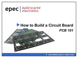
PCB 101 - How To Build a Circuit Board
•Als PPT, PDF herunterladen•
30 gefällt mir•23,828 views

Our PCB 101 Presentation goes through the processes involved in manufacturing a printed circuit board. From a simple single sided board to a complex multi-layer, double sided surface mount design, our goal is to provide you a design that meets your requirements and is the most cost effective to manufacture. Our experience in IPC Class III standards, very stringent cleanliness requirements, heavy copper and production tolerances allow us to provide our customers exactly what they need for their end product.

Empfohlen
Weitere ähnliche Inhalte
Was ist angesagt?
Was ist angesagt? (20)
Andere mochten auch
Andere mochten auch (15)
Ähnlich wie PCB 101 - How To Build a Circuit Board
Ähnlich wie PCB 101 - How To Build a Circuit Board (20)
Mehr von Epec Engineered Technologies
Mehr von Epec Engineered Technologies (20)
Kürzlich hochgeladen
Kürzlich hochgeladen (20)
PCB 101 - How To Build a Circuit Board
- 1. How to Build a Circuit Board PCB 101 DELIVERING QUALITY SINCE 1952.
- 2. America's Oldest, A History of Innovation Privately held company, established in 1952. Estimated 2013: Sales: US$40 Million 100+ Employees Worldwide (70 – North America, 30 – Asia, 3 – Europe) Design and manufacture customized, built-to-print, performance-critical products for all sectors of the electronics industry. Leading provider of printed circuit boards, membrane switches, graphic overlays, silicone rubber products, electronic heaters, fans, motors and custom battery packs. Integrated supply chain management solutions to handle the complexity of today’s global marketplace while making sure that every order is being manufactured at the “right” factory. 2
- 3. Global Operations Significant Investment in People and Facilities across the globe. 3
- 4. Our Customers - The Top Global OEM’s In Growth Industries 4
- 5. Our Products Battery Packs Flex & Rigid-Flex PCB’s User Interfaces Fans & Motors Cable Assemblies Printed Circuit Boards 5
- 6. PCB Design and Layout Our Capabilities Encompass The Full Design Flow From Start To Finish Including: Micro BGA / Micro Via / Blind and Buried Vias Rules Driven Designs Schematic Capture Library Development Database Construction and Verification Signal Integrity/Design Verification EMI Checking Full Document Package Creation Electrical Engineering Expertise We are fully licensed and utilize industry leading tools, including Cadence Allegro, Mentor Expedition, Mentor's PADS, Altium, Valor for DFM Analysis. 6
- 7. How to Build a Circuit Board PCB 101 Customer Supplied Data – CAD • ODB++, Gerber, Gerber 274X • Netlist (IPC-D-356) – Drawing Package • Fabrication drawing • Readme File • Specifications 7
- 8. How to Build a Circuit Board PCB 101 Cam Deliverables – Conversion of Customer Supplied Data to Tooling Panelization – Optimized manufacturing Panel – Customer defined sub-panels or arrays Artwork – – – – Inner Layer Outer Layer Soldermask Legend Drill and Rout Programs – Excellon format ASCII 8
- 9. How to Build a Circuit Board PCB 101 Engineering Strategy – Epec’s Front End Engineering Department uses state of the art software to identify and reduce or eliminate unnecessary manufacturing costs. EpecDFx - Perfecting the DFM Process – EpecDFx goes beyond DFM (Design for Manufacturability) • Design for cost • Design for functionality – ALL jobs are processed through EpecDFx checking for: • Shorts • Opens • Line widths • Spacing issues • Mask problems • Legend problems • Inner layer plane problems • Controlled impedance • Unused pads (and removal of same) 9
- 10. How to Build a Circuit Board PCB 101 Cores/Laminate – A thin laminate material (usually under .250” thick) consisting of a glass epoxy substrate clad with copper on both sides. – The size of the core is larger than the finished size of the board. Copper Foil Laminate 10
- 11. How to Build a Circuit Board PCB 101 Laminate: CEM-1 Low cost – Single Sided Industry standard for low cost single sided PWB. – Material of choice for low cost, single sided PWB applications – Suitable for low to moderate board rigidity requirements (lowest rigidity of these three laminates) – May not be suitable in environments where moisture absorption is of high concern COPPER FOIL CEM-1: A 5-ply composite composed of one ply of epoxy-resin impregnated glass cloth above and below a 3-ply epoxy-resin coated paper core. EPOXY-RESIN GLASS CLOTH 3-PLY KRAFT PAPER CREATING AN EPOXY-RESIN COATED PAPER CORE EPOXY-RESIN GLASS CLOTH 11
- 12. How to Build a Circuit Board PCB 101 Laminate: FR-4 – Industry Standard Rigid PWB Laminate – FR-4 is truly the most generic laminate – Many different manufacturers offer products with different characteristics COPPER FOIL FR-4: Eight weaves of fiberglass cloth laminated together with an epoxy resin. (60% Glass / 40% Resin) EIGHT WEAVES OF FIBERGLASS CLOTH LAMINATED TOGETHER WITH AN EPOXY RESIN COPPER FOIL 12
- 13. How to Build a Circuit Board PCB 101 Dry Film Resist Coat – A light sensitive film is applied by heat and pressure to the copper surfaces of the core Photo Tools & Artwork – These are placed on the film coated surfaces of the core – Artwork patterns are customer designs containing circuit and land patterns specific to that part number – Each surface has its own artwork pattern Etch Photoresist 13
- 14. How to Build a Circuit Board PCB 101 Expose – Panels are exposed to ultra-violet light – Clear areas allow light to pass through and polymerize (harden) the film resist thus creating a latent image of the circuit pattern Develop – The exposed core is passed through a chemical solution removing the resist from areas not hardened (polymerized) Artwork 14
- 15. How to Build a Circuit Board PCB 101 Etch – Copper is chemically removed from the core in all areas not covered by film resist – This creates a discrete copper pattern – Core surface now shows through in areas where copper was etched away 15
- 16. How to Build a Circuit Board PCB 101 Strip Resist – The developed dry film resist is now chemically removed from the panel – Copper remains on the panel only in the patterns described by artwork 16
- 17. How to Build a Circuit Board PCB 101 Oxide Coating – Copper is chemically treated to “rough-up” surface – Rough surface improves adhesion to prepreg during the lamination cycle – Oxide is typically black, though other types exist, i.e. Brown and Red 17
- 18. How to Build a Circuit Board PCB 101 Multilayer Lamination – Materials Needed: • Copper Foil • Prepreg • Cores Prepreg – Multilayer “glue” – Fiberglass cloth preimpregnated with partially cured epoxy resin – Also known as B-stage Copper Foil – Typically in sheets at ½ oz. or 1 oz. per square foot in weight (.0007 and .0014 inches nominal thickness respectively) 18
- 19. How to Build a Circuit Board PCB 101 Laminated Blank – Inner Layer Core, Copper Foil and Prepreg are bonded together under heat and pressure, usually in a vacuum, during the lamination process – Prepreg resin is activated and “melts”, flowing across the layer to create a bond. – Half-sheets are produced during this step – Half-sheets are then cut or fabricated (fabed) into panel size Primary Drilling – Double Sided/Single Sided Start here • Holes are drilled through a stack of panels (usually 2 to 3 high) • Drilled holes are typically .005” larger than finished plated through hole size 19
- 20. How to Build a Circuit Board PCB 101 Drill – Holes are CNC drilled to specific coordinates from the data supplied after it is formatted Inner Layer Laminate Copper Foil 20
- 21. How to Build a Circuit Board PCB 101 Multilayer Stack-up (Cross Section) 4 Layer 6 Layer Copper Foil (.5, 1, 2, ... ounces) Double sided core (.028 for 4 layer) (.014 for 6 layer) (.008 for 8 layer) Copper weight up to 3 ounces B-stage Prepreg (Bonding Sheets) 8 Layer 21
- 22. How to Build a Circuit Board PCB 101 Deburr & Clean – A mechanical process where copper burs are removed from the panel – All debris is cleaned from drill holes Desmear – Applies to multilayer boards only – A chemical process where the coating of resin, produced by the heat of drilling, is removed from the hole wall 22
- 23. How to Build a Circuit Board PCB 101 Copper Deposition – – – – Also called electroless copper A thin coating is chemically deposited on the surface of the panel and hole walls This creates a metallic base for subsequent electroplating operations Typically thickness is 80-100 millionths of an inch Electroless Copper 23
- 24. How to Build a Circuit Board PCB 101 Dry Film Photo Resist Coat – The panel is pre-cleaned – Light sensitive film is applied, using heat and pressure, to the copper surfaces of the laminated “blank” – Film also covers, or tents, all drilled holes Inner Layer Laminate Copper Foil 24
- 25. How to Build a Circuit Board PCB 101 Expose & Develop – The panel is then exposed and developed – Similar to the inner layer process for the core – Holes that are to be plated have tents developed off Photoresist Artwork 25
- 26. How to Build a Circuit Board PCB 101 Copper Pattern Plate – – – – – Also called electroplating Additional copper is electrically plated onto the exposed electroless copper surfaces Copper thickness is approximately 1 mil Tin is also plated onto all copper surfaces Typical tin thickness is .3 - .5 mils Electroplated Copper Resist Metal (tin) 26
- 27. How to Build a Circuit Board PCB 101 Etch – Copper is now removed any place not covered by tin – The tin acts as an etch resist – Traces and pads, as defined by the artwork, are now left on the surface of the panel 27
- 28. How to Build a Circuit Board PCB 101 Strip Resist – The developed dry film resist is now chemically removed from the panel – Tents that were placed have prevented plating to occur in holes designed to be non-plated 28
- 29. How to Build a Circuit Board PCB 101 Solder Mask & Cure – A Liquid Photo Imagable mask, is applied to each surface and dried to the touch, – – – – – – but not cured Artwork is applied and exposed Panel is developed, leaving mask in pattern described by artwork Panels are cure baked Mask protects panels from contamination and handling damage Solder mask is a non-conductive material Laminate is a natural color, solder mask gives the circuit board its final color, typically green Solder Mask 29
- 30. How to Build a Circuit Board PCB 101 Hot Air Solder Leveling (HASL) – Panels are processed thru a bath of molten solder, covering all exposed copper surfaces – High pressure hot air, directed at both sides of the panel simultaneously, removes excess solder from the holes and surfaces – While HASL is still the most common PCB surface finish, many other options exist that will allow our customers to meet their end product needs. Solder 30
- 31. How to Build a Circuit Board PCB 101 Surface Finishes – RoHS Compliant: • • • • • • • • Organic Solder Preservation (OSP) Single and Multi-Pass Lead-free HASL Nickel Plate Nickel/Gold Palladium – Nickel Immersion Tin Immersion Silver – Not RoHS Compliant: • Hot Air Solder Leveling (HASL) 31
- 32. How to Build a Circuit Board PCB 101 OSP Surface Finishes – Single-Pass – single soldering operation (or heat cycle) – Multi-Pass - able to survive multiple heat excursions for SMT applications – Coating is molecular in thickness and is compatible with most flux systems, including “no wash” systems – DOES NOT CONTAIN LEAD! 32
- 33. How to Build a Circuit Board PCB 101 Lead Free HASL – There are several types • SN100 (most common in China) – Tin – trace of Copper < 0.7% • SAC305 – Limited availability – Tin – 3.0% Silver - .05% Copper – PCB is conveyed through the flux station, then through the solder bath and finally through a set of air knives that remove (level) excess solder – Thickness varies - Generally somewhat thinner than regular HASL: • From .000100” to .001500” – Lead Free HASL provides a solderable surface with most flux systems and is also suitable for most surface mount applications 33
- 34. How to Build a Circuit Board PCB 101 Ni / Au Plating – Electroplated Deposit • SMOBC – soldermask used as plating resist • We will only plate Ni/Au after etching – we will not use Ni/Au as an etching resist • All circuits or features which will be electrically connected with plating buss (tie bars) • Thickness for Gold: .000005” to .000050” – ENIG – Electroless Nickel/Immersion Gold • Bussing (tie bars) not required • Max. Thickness for Gold: .000002” to .000005” 34
- 35. How to Build a Circuit Board PCB 101 Immersion Tin (Also known as White Tin) – Excellent Co-planarity – Shelf life equal to or exceeds HASL – Will solder after multiple heat cycles – Solder paste, reflow, glue dot and wave soldering – Less dimensional stress than with HASL – No special handling required 35
- 36. How to Build a Circuit Board PCB 101 Immersion Silver – – – – – Totally flat topography More solderable than copper Does not require special handling like OSP (white gloves, etc.) Shelf life is 6-12 months depending on storage conditions Can withstand 5 temperature cycles 36
- 37. How to Build a Circuit Board PCB 101 Hot Air Leveling (HAL, HASL) 63/37 Solder Coating – PCB is conveyed through the flux station, then through the solder bath and finally through a set of air knives that remove (level) excess solder – Thickness varies: • From .000100” to .001500” – HASL provides a solderable surface for all flux systems and is also suitable for surface mounted applications – Still the most common protective coating used in PCB manufacturing 37
- 38. How to Build a Circuit Board PCB 101 Legend & Cure – Ink is silkscreened onto each side of the panel as described by customer artwork – The printing details component placement and other surfaces details desired by the customer – Panels are baked to cure the ink Legend & SMT Nomenclature Legends can create problems for the PCB manufacturers. – Many designers put a box completely surrounding SMT pads to indicate component placement – Often the tolerances required to screen print legend are not considered. Avoid narrow fonts, text height less than .040” and trace width below .006” – Ask your designer to provide adequate clearances around SMT pads 38
- 39. How to Build a Circuit Board PCB 101 Legend Placement Around SMD Pads Too Tight Good 39
- 40. How to Build a Circuit Board PCB 101 Fabrication / Routing – The board is cut to size – Also known as routing, scoring, punching or profiling – Chamfers and slots are also added during this step 40
- 41. How to Build a Circuit Board PCB 101 V-Groove Scoring Engineers see scoring as a way to save. It does save from a material utilization basis, but there are tradeoffs. Tolerances must be relaxed on the finished piece part to allow for these tolerances. Furthermore, scoring has one of the highest fallout rates of any process in manufacturing. Score line to Score line +/-.005” Score line to holes +/-.007” Score line to Artwork .015 - .020 Finished part tolerance +.015/-.010 Web Remaining +/-.005” Typical Web remaining for each laminate CEM-1 .030” CEM-3 .030” FR-4 .015” HIGH Tg FR-4 .012” 41
- 42. How to Build a Circuit Board PCB 101 V-Groove Scoring Scoring: Usually defined as “Web remaining.” This defines the amount of material remaining. The cutter has a 30 degree included angle. (45 and 60 degree cutters available) * Note how the width of the score line changes with the depth of cut. 0.008 Typical for FR-4 0.010 0.015 0.013 0.030 Typical for CEM1 and CEM-3 0.012 42
- 43. How to Build a Circuit Board PCB 101 Copper Weight vs. Minimum Spaces – – – – – 1 ounce copper - .008” between adjacent features 2 ounce copper - .010” between adjacent features 3 ounce copper - .012” between adjacent features 4 ounce copper - .015” between adjacent features 6 ounce copper - .020” between adjacent features 43
- 44. How to Build a Circuit Board PCB 101 Electrical Test – – – – – Board is tested for electrical integrity, and if required, impedance Data can be directly loaded from CAM to test machines in some cases Most tests are feasible. Repairs of shorts and opens are also done at this point Smaller lots tested on a flying probe, larger volume on a bed of nails test fixture IPC Netlist is used if supplied by the Customer 44
- 45. How to Build a Circuit Board PCB 101 Functions Performed Throughout the Process: – AOI • Automatic Optical Inspection • Inner layers and outer layers are tested against downloaded CAM data for integrity, and against design rules • If allowed and feasible, repairs are made at this point • Data is fed back to appropriate departments to correct process problems 45
- 46. How to Build a Circuit Board PCB 101 Functions Performed Throughout the Process: – Reliability Lab • In-house capability to test for compliance to many customer and industry requirements • Environmental Cycling, Ionic Contamination, Surface Insulation Resistance are a few tests performed. • Data is fed back to departments and customers as required 46
- 47. How to Build a Circuit Board PCB 101 Functions Performed Throughout the Process: – SPC • Statistical Process Control • Method used both on and off-line to determine if process and product is performing as expected • ONLY reliable method to make process changes • Often required by customers 47
- 48. How to Build a Circuit Board PCB 101 PCB Design Concerns – Hole Size • >10 Mils drilled standard • 8 – 9 Mils, leading edge • 5 Mils, bleeding edge • Note: Drilled hole size typically is .003”-.005’ larger than FHS PCB Design Concerns – Line/Space • 5/5 standard • 3/3 leading edge – Aspect Ratio • 8:1 standard – 0.080” min hole size for 0.062” – Pad Size • 10 Mils over drilled hole • 12:1 leading edge – 0.005” hole for 0.062” diameter standard • 8 Mils leading edge • PWG/GRD Clearance – 20 mils over drill 48
- 49. How to Build a Circuit Board PCB 101 PCB Manufacturing Concerns 4 Layer Off Center Construction .024” .024” .006” Warpage Issues Meets flatness specification 49
- 50. How to Build a Circuit Board PCB 101 Manufacturing / Design Concerns Plating – External copper thieving is recommended to be added to low-density areas to even out copper distribution. Typical thieving pattern is .030” squares on .050” centers. – The absence of copper thieving result in high, or over plating of isolated features, typically differential pairs. It can also cause pitted appearance on fiducial pads, which will cause assembly problems. 50
- 51. How to Build a Circuit Board PCB 101 Panelization – PWB’s are manufactured on standard – – – – panel sizes Cost is a factor of the number of individual cards on a production panel Impedance/Mil coupons, if required, are placed in the production panel May effect panelization yield, i.e. $$ Industry standard panel size is 18” x 24” General rule: • 0.750” border all 4 edges • 0.100” spacing between images 51
- 52. How to Build a Circuit Board PCB 101 Sample Fabrication Drawings/Notes 52
- 53. How to Build a Circuit Board PCB 101 Price Considerations – Low Cost Factors • • • • • Complex Routing/Scoring Edge Routing >0.093” Thick PWB’s <0.030” Thick PWB’s High Tg vs. low Tg Materials – High Cost Factors • • • • • • Advanced Technologies Buried Vias Layer Count Material Utilization Selective Plating Line Width and Space – Medium Cost Factors • • • • High Drill Hole Quantity Plated hole tolerance less than +/- 0.003” Edge Plating Drilled holes <0.010” 53
- 54. Industry’s Leading Online Tools Sign up today and try InstantPCBQuote™, the most flexible and user friendly internet quoting and ordering tool in the PCB industry. Try it Now! www.epectec.com/instantpcbquote 54
- 55. World Class Quality Assurance & Engineering US Based QA Capabilities Include: – Full Cross Section/Microsection Reporting and – – – – Ionic Testing Equipment X-Ray Fisherscope for all Metal Thickness & Purity Measurement on every lot. Scienscope DMP-1000 stereo zoom microscope with digital picture capability up to 100x Vision Engineering Mantis Elite for 10X full range visual inspection. World Class Electronics Test Lab Epec’s superior on-time delivery rates are the result of our significant, dedicated engineering resources and processes. – Perform all DRC, DFM, Graphic Art and Engineering reviews at our Engineering Center outside of Boston, MA – Documentation of all manufacturing and detailed planning processes, for all special requirements, – Consistent documentation and tooling at all manufacturing locations to ensure seamless prototype through production manufacturing. 55
- 56. Design Centers & Technical Support Battery Pack & Power Management – Denver, CO User Interfaces – Largo, FL Fans & Motors – Wales, UK PCB’s – New Bedford, MA & Shenzhen, China Flex & Rigid Flex – Toronto, Canada Cable Assemblies – New Bedford, MA Heaters & Sensors – Boston, MA Our Engineering and Design teams are ready to help our customers create world class and cost effective product solutions. 56
- 57. Inventory Management Customer requirements are always unique and customized, therefore our inventory management system must accommodate for this type of environment. We Offer: – Kanban – Consignment – JIT Programs – Blanket Orders – Customer Fulfillment – Bonded Warehousing – Kitting – Safety Stock – Other flexible solutions 57
- 58. The Difference is Quality and Delivery 1. Quicker Delivery - Epec's technology infrastructure and people, including the Asian and US based operations, manufacturing and engineering teams, enable jobs to get started the same day the order is received with no delays. 2. Accurate Information - Epec's proven supply chain and manufacturing experience allows accurate daily Work In Process reporting so customers can receive immediate order status information. 3. Better Quality - Epec ensures higher levels of quality through actual investment in all of our processes. Whether it is our 10+ people strong quality organization in Asia, equiping our tech centers with the latest tech gear to test parts, or our continuous improvement auditing process, real investment is made to ensure quality. 4. Flexibility - Each of our manufacturing facilities have been selected for their best-in-class niche product and delivery and techology solutions, ensuring our optimal facility is building every order. 58
- 59. If you require additional information please contact us with any questions or requests. North American Headquarters 174 Duchaine Blvd. New Bedford, MA 02745 Tel: (508) 995-5171 Fax: (508) 998-8694 Contact Us By Email: Sales Quotes Engineering sales@epectec.com quoting@epectec.com engineering@epectec.com Visit Our Website For More Information www.epectec.com Stay Connected with Epec Engineered Technologies Join our Social Community and keep in touch with all our latest technology investments, current news, upcoming events, and promotions. Visit our Social Media Websites for more information. 59