SlideShare a Scribd company logo
1 of 3
Download to read offline
Access this lab-manual at:
http://www.docircuits.com/lab-manual/52/vi-characteristics-of-diode
VI Characteristics of Diode
Diode Forward Characteristics...

P-N Junction Reverse Bias Char...

Aim
Aim is to
1. Explain the structure of a P-N junction diode
2. Explain the function of a P-N junction diode
3. Explain forward and reverse biased characteristics
of a Silicon diode

Related Experiments
DIODE

Description
Theory:
The term bias refers to the use of a dc voltage to establish certain operating conditions for an electronic device.
Depending on the magnitude and polarity of the applied voltage the diode is said to be:
Forward Biased, Anode voltage is greater than the Cathode voltage
Reverse Biased, Cathode voltage is greater than the Anode voltage
So, diode is a simple switch that is either closed (conducting) or open (non conducting). Specifically, the diode is a
short circuit, like a closed switch, when voltage is applied in the forward direction, and an open circuit, like an
open switch, when the voltage is applied in the reverse direction.
Let us now take the earlier model one more step. The offset voltage model adds the barrier potential to the ideal
switch model. When the diode is forward biased it is equivalent to a closed switch in series with a small equivalent
voltage source equal to the barrier potential (0.7 V for Silicon, 0.4 for germanium) with the positive side towards the
anode. When the diode is reverse biased, it is equivalent to an open switch just as in the ideal model.

When forward biased, Vg ( 0.7 for Silicon and 0.4 for Germanium ) volts appears across the diode and current flows.

During reverse bias, when the voltage applied across the diode is less than Vg, there will be no current flowing.
Let us now take the earlier model one more step. It is the most accurate of the diode models. The Complete diode
model of a diode consists of the barrier potential, the small forward dynamic resistance and the ideal diode. The
resistor approximates the semiconductor resistance under forward bias. This diode model most accurately
represents the true operating characteristics of the real diode.

¨Static Resistance of a P-N junction diode is the ratio of forward voltage to forward current
¨Dynamic Resistance of a P-N junction diode is the small change in forward voltage to small change in
forward current at a particular operating point.
When a diode is reverse biased a leakage current flows through the device. This current can be effectively ignored

REVERSE

CHARACTERISTICS
When a diode is reverse biased a leakage current flows through the device. This current can be effectively ignored
as long as the reverse breakdown voltage of the diode is not exceeded. At potentials greater than the reverse
breakdown voltage, charge is pulled through the p-n junction by the strong electric fields in the device and large
reverse current flows. This usually destroys the device. There are special diodes that are designed to operate in
breakdown. Such diodes are called zener diodes and used as voltage regulators.

¨Take Resistor of 1Kohms
¨Connect to Si Diode.
¨Use Ammeter to measure current and Voltmeter to measure Voltage
¨Setup the circuit as shown

¨One way to measure the VI Characteristics of the diode is the set the DC source at various voltage levels
¨Note the current in the ammeter and voltage in the voltmeter
¨Plot the current against voltage
¨Instead of re-running the experiment at various voltage values from DC source, let us parameterize
¨Click on Simulation Properties – DC Analysis
¨Choose DC Source and Vary the voltage from 0V to 5V to record the voltage and current across the diode
¨Run the experiment
¨On successful run, click on Data Analysis to view the current and the voltage readings
¨Choose to plot against the voltage the current.
¨Edit the properties of the graph to view a closer segment of the plot

¨Select 0.4 V to 1.0 V on the X Axis with interval of 0.01 V
¨On the zoomed graph – measure the
¨Cut off Voltage
¨Static Resistance
¨Dynamic Resistance
¨Hint – to calculate Static and Dynamic Resistances
¨Zoom in the Y axis as well.
¨Dynamic Resistance = Slope of the graph for a particular point
Reverse-bias characteristics
¨Setup the circuit as before – but reverse the diode in the circuit so that it is reversed biased.
¨Go through the same steps as before to record the Current and Voltage Readings but the stop voltage should
be about 60 V.
¨Note that maximum current flows after about 50 V in the reverse direction..

¨

Conclusion
Thus the forward and reverse bias characteristics of the diode have been verified and plotted.
VI Characteristics of Diode

More Related Content

What's hot

Pn junction diode characteristics Lab expriment
Pn junction diode characteristics Lab exprimentPn junction diode characteristics Lab expriment
Pn junction diode characteristics Lab exprimentdhanajeyan dhanaj
 
Semiconductor diodes
Semiconductor diodesSemiconductor diodes
Semiconductor diodesSirat Mahmood
 
Different semiconductor diodes.ppt
Different semiconductor diodes.pptDifferent semiconductor diodes.ppt
Different semiconductor diodes.pptSHASHIKUMARDASI
 
The p n Junction Diode (Basic Electronics)
The p n Junction Diode (Basic Electronics) The p n Junction Diode (Basic Electronics)
The p n Junction Diode (Basic Electronics) Ivan Saguit
 
Diode v i characteristic
Diode v i characteristicDiode v i characteristic
Diode v i characteristicUnsa Shakir
 
Physics Investigatory:To Study V-I Characteristics Of Zener Diode
Physics Investigatory:To Study V-I Characteristics Of Zener DiodePhysics Investigatory:To Study V-I Characteristics Of Zener Diode
Physics Investigatory:To Study V-I Characteristics Of Zener DiodeGautammaini9
 
Full sessional pack ii
Full sessional pack iiFull sessional pack ii
Full sessional pack iiUmer Tanvir
 
Tunnel Diode (Esaki Diode )
Tunnel Diode (Esaki Diode )Tunnel Diode (Esaki Diode )
Tunnel Diode (Esaki Diode )Soudip Sinha Roy
 
Best 3 Applications Involving in Zener Diode Working Functionality
Best 3 Applications Involving in Zener Diode Working FunctionalityBest 3 Applications Involving in Zener Diode Working Functionality
Best 3 Applications Involving in Zener Diode Working Functionalityelprocus
 

What's hot (20)

Diodes
DiodesDiodes
Diodes
 
Pn junction diode characteristics Lab expriment
Pn junction diode characteristics Lab exprimentPn junction diode characteristics Lab expriment
Pn junction diode characteristics Lab expriment
 
Special purpose diode
Special purpose diodeSpecial purpose diode
Special purpose diode
 
Semiconductor diodes
Semiconductor diodesSemiconductor diodes
Semiconductor diodes
 
Different semiconductor diodes.ppt
Different semiconductor diodes.pptDifferent semiconductor diodes.ppt
Different semiconductor diodes.ppt
 
The p n Junction Diode (Basic Electronics)
The p n Junction Diode (Basic Electronics) The p n Junction Diode (Basic Electronics)
The p n Junction Diode (Basic Electronics)
 
Diode v i characteristic
Diode v i characteristicDiode v i characteristic
Diode v i characteristic
 
Pn junction diode
Pn junction diodePn junction diode
Pn junction diode
 
Semiconductor diode
Semiconductor diodeSemiconductor diode
Semiconductor diode
 
PN JUNCTION
PN JUNCTION PN JUNCTION
PN JUNCTION
 
Zener diodes
Zener diodesZener diodes
Zener diodes
 
Pn junction
Pn junctionPn junction
Pn junction
 
Diode theory
Diode theoryDiode theory
Diode theory
 
2 diode applications
2 diode applications2 diode applications
2 diode applications
 
Edtech2
Edtech2Edtech2
Edtech2
 
diode technology
diode technologydiode technology
diode technology
 
Physics Investigatory:To Study V-I Characteristics Of Zener Diode
Physics Investigatory:To Study V-I Characteristics Of Zener DiodePhysics Investigatory:To Study V-I Characteristics Of Zener Diode
Physics Investigatory:To Study V-I Characteristics Of Zener Diode
 
Full sessional pack ii
Full sessional pack iiFull sessional pack ii
Full sessional pack ii
 
Tunnel Diode (Esaki Diode )
Tunnel Diode (Esaki Diode )Tunnel Diode (Esaki Diode )
Tunnel Diode (Esaki Diode )
 
Best 3 Applications Involving in Zener Diode Working Functionality
Best 3 Applications Involving in Zener Diode Working FunctionalityBest 3 Applications Involving in Zener Diode Working Functionality
Best 3 Applications Involving in Zener Diode Working Functionality
 

Viewers also liked

High Power TVS Overvoltage Protection Diodes
High Power TVS Overvoltage Protection DiodesHigh Power TVS Overvoltage Protection Diodes
High Power TVS Overvoltage Protection DiodesPremier Farnell
 
1.1.4 v i characteristics of diode
1.1.4 v i characteristics of diode1.1.4 v i characteristics of diode
1.1.4 v i characteristics of diodeLearn By Watch
 
Pn junction diodes (presentation)
Pn junction diodes (presentation)Pn junction diodes (presentation)
Pn junction diodes (presentation)Alan Bullard
 
Drawing exploded & sectional detail
Drawing exploded & sectional detailDrawing exploded & sectional detail
Drawing exploded & sectional detailShar Shar
 
P-N Junction Diode Submitted By Aditya Prata
P-N Junction Diode Submitted By Aditya Prata P-N Junction Diode Submitted By Aditya Prata
P-N Junction Diode Submitted By Aditya Prata Aditya Pratap Singh
 
1.1.6 diode resistance
1.1.6 diode resistance1.1.6 diode resistance
1.1.6 diode resistanceLearn By Watch
 
P-N junction
P-N junctionP-N junction
P-N junctionblackboX
 
projection of Sectional view-engineering drawing b.tech
projection of Sectional view-engineering drawing b.techprojection of Sectional view-engineering drawing b.tech
projection of Sectional view-engineering drawing b.techMohd Mujahid Nasir
 
P n junction characteristics
P n junction characteristicsP n junction characteristics
P n junction characteristicsAshvani Shukla
 
Pn diode for aitm sanjay
Pn diode for aitm sanjayPn diode for aitm sanjay
Pn diode for aitm sanjaySanjay Jangra
 
P n junction diode
P n junction diodeP n junction diode
P n junction diodeHarsh Vijay
 
Circuit and analog electronics ch6
Circuit and analog electronics ch6  Circuit and analog electronics ch6
Circuit and analog electronics ch6 Nadhiien Abraham
 

Viewers also liked (20)

Diodes
DiodesDiodes
Diodes
 
High Power TVS Overvoltage Protection Diodes
High Power TVS Overvoltage Protection DiodesHigh Power TVS Overvoltage Protection Diodes
High Power TVS Overvoltage Protection Diodes
 
Semiconductor physics
Semiconductor physicsSemiconductor physics
Semiconductor physics
 
1.1.4 v i characteristics of diode
1.1.4 v i characteristics of diode1.1.4 v i characteristics of diode
1.1.4 v i characteristics of diode
 
Pn junction diodes (presentation)
Pn junction diodes (presentation)Pn junction diodes (presentation)
Pn junction diodes (presentation)
 
Pop Culture, Sustainability & Innovation
Pop Culture, Sustainability & InnovationPop Culture, Sustainability & Innovation
Pop Culture, Sustainability & Innovation
 
Mod3
Mod3Mod3
Mod3
 
Heat capacity of solids
Heat capacity of solidsHeat capacity of solids
Heat capacity of solids
 
Drawing exploded & sectional detail
Drawing exploded & sectional detailDrawing exploded & sectional detail
Drawing exploded & sectional detail
 
P-N Junction Diode Submitted By Aditya Prata
P-N Junction Diode Submitted By Aditya Prata P-N Junction Diode Submitted By Aditya Prata
P-N Junction Diode Submitted By Aditya Prata
 
1.1.6 diode resistance
1.1.6 diode resistance1.1.6 diode resistance
1.1.6 diode resistance
 
P-N junction
P-N junctionP-N junction
P-N junction
 
Adc
AdcAdc
Adc
 
projection of Sectional view-engineering drawing b.tech
projection of Sectional view-engineering drawing b.techprojection of Sectional view-engineering drawing b.tech
projection of Sectional view-engineering drawing b.tech
 
DIODES
DIODESDIODES
DIODES
 
P n junction characteristics
P n junction characteristicsP n junction characteristics
P n junction characteristics
 
Presentation project6
Presentation project6Presentation project6
Presentation project6
 
Pn diode for aitm sanjay
Pn diode for aitm sanjayPn diode for aitm sanjay
Pn diode for aitm sanjay
 
P n junction diode
P n junction diodeP n junction diode
P n junction diode
 
Circuit and analog electronics ch6
Circuit and analog electronics ch6  Circuit and analog electronics ch6
Circuit and analog electronics ch6
 

Similar to VI Characteristics of Diode

Similar to VI Characteristics of Diode (20)

JUNCTION DIODE APPLICATIONS
JUNCTION DIODE APPLICATIONSJUNCTION DIODE APPLICATIONS
JUNCTION DIODE APPLICATIONS
 
task_2.pptx
task_2.pptxtask_2.pptx
task_2.pptx
 
PE4MSc_Ch1_SC_devices.pptx
PE4MSc_Ch1_SC_devices.pptxPE4MSc_Ch1_SC_devices.pptx
PE4MSc_Ch1_SC_devices.pptx
 
227 sample chapter
227 sample chapter227 sample chapter
227 sample chapter
 
Diode Application
Diode ApplicationDiode Application
Diode Application
 
Tanya makkar (5003)
Tanya makkar (5003)Tanya makkar (5003)
Tanya makkar (5003)
 
Basic electronics (p-n Junction)
Basic electronics (p-n Junction)Basic electronics (p-n Junction)
Basic electronics (p-n Junction)
 
Diode and its Applications
Diode and its Applications Diode and its Applications
Diode and its Applications
 
EDC LAB MASTER MANUAL AY 22-23.doc
EDC LAB MASTER  MANUAL AY 22-23.docEDC LAB MASTER  MANUAL AY 22-23.doc
EDC LAB MASTER MANUAL AY 22-23.doc
 
Lecture-2.pptx
Lecture-2.pptxLecture-2.pptx
Lecture-2.pptx
 
Experiment no 9
Experiment no 9Experiment no 9
Experiment no 9
 
Zener diode experiment.
Zener diode experiment.Zener diode experiment.
Zener diode experiment.
 
Bsc 1 cbcs e1 unit 2
Bsc 1 cbcs e1 unit 2Bsc 1 cbcs e1 unit 2
Bsc 1 cbcs e1 unit 2
 
Eg1108 rectifiers
Eg1108 rectifiersEg1108 rectifiers
Eg1108 rectifiers
 
A study of 220V AC-5V DC Converter
A study of 220V AC-5V DC ConverterA study of 220V AC-5V DC Converter
A study of 220V AC-5V DC Converter
 
ADE Unit1.pptx
ADE Unit1.pptxADE Unit1.pptx
ADE Unit1.pptx
 
adeunit1-221223065954-a64adaae.pdf
adeunit1-221223065954-a64adaae.pdfadeunit1-221223065954-a64adaae.pdf
adeunit1-221223065954-a64adaae.pdf
 
Electronic devices circuits
Electronic devices circuitsElectronic devices circuits
Electronic devices circuits
 
B02010711
B02010711B02010711
B02010711
 
Lecture Two.pptx
Lecture Two.pptxLecture Two.pptx
Lecture Two.pptx
 

More from DoCircuits

Inverting Amplifier : Op-amp
Inverting Amplifier : Op-ampInverting Amplifier : Op-amp
Inverting Amplifier : Op-ampDoCircuits
 
Half Subtractor : Combiational Circuit
Half Subtractor : Combiational CircuitHalf Subtractor : Combiational Circuit
Half Subtractor : Combiational CircuitDoCircuits
 
Half Wave Rectifier
Half Wave RectifierHalf Wave Rectifier
Half Wave RectifierDoCircuits
 
Common Emitter Amplifier : BJT
Common Emitter Amplifier : BJTCommon Emitter Amplifier : BJT
Common Emitter Amplifier : BJTDoCircuits
 
Common Collector Amplifier : BJT
Common Collector Amplifier : BJTCommon Collector Amplifier : BJT
Common Collector Amplifier : BJTDoCircuits
 
Common Base Amplifier - BJT
Common Base Amplifier - BJTCommon Base Amplifier - BJT
Common Base Amplifier - BJTDoCircuits
 
Half Adder - Combinational Circuit
Half Adder - Combinational CircuitHalf Adder - Combinational Circuit
Half Adder - Combinational CircuitDoCircuits
 
Bridge Rectifier
Bridge RectifierBridge Rectifier
Bridge RectifierDoCircuits
 
Common Source Characteristics - JFET
Common Source Characteristics - JFETCommon Source Characteristics - JFET
Common Source Characteristics - JFETDoCircuits
 
JFET common drain characteristics
JFET common drain characteristicsJFET common drain characteristics
JFET common drain characteristicsDoCircuits
 
Bridge Rectifier with Capacitor filter
Bridge Rectifier with Capacitor filterBridge Rectifier with Capacitor filter
Bridge Rectifier with Capacitor filterDoCircuits
 
Voltage Divider Bias - BJT
Voltage Divider Bias - BJTVoltage Divider Bias - BJT
Voltage Divider Bias - BJTDoCircuits
 
BJT characteristics
BJT characteristicsBJT characteristics
BJT characteristicsDoCircuits
 
36.voltage divider bias
36.voltage divider bias36.voltage divider bias
36.voltage divider biasDoCircuits
 
34.fixed bias without re
34.fixed bias without re34.fixed bias without re
34.fixed bias without reDoCircuits
 
Using Cloud based simulation for learning Electronics using DoCircuits
Using Cloud based simulation for learning Electronics using DoCircuitsUsing Cloud based simulation for learning Electronics using DoCircuits
Using Cloud based simulation for learning Electronics using DoCircuitsDoCircuits
 

More from DoCircuits (20)

33
3333
33
 
Inverting Amplifier : Op-amp
Inverting Amplifier : Op-ampInverting Amplifier : Op-amp
Inverting Amplifier : Op-amp
 
Half Subtractor : Combiational Circuit
Half Subtractor : Combiational CircuitHalf Subtractor : Combiational Circuit
Half Subtractor : Combiational Circuit
 
Half Wave Rectifier
Half Wave RectifierHalf Wave Rectifier
Half Wave Rectifier
 
Diode Clippers
Diode ClippersDiode Clippers
Diode Clippers
 
Diode Clampers
Diode ClampersDiode Clampers
Diode Clampers
 
Common Emitter Amplifier : BJT
Common Emitter Amplifier : BJTCommon Emitter Amplifier : BJT
Common Emitter Amplifier : BJT
 
Common Collector Amplifier : BJT
Common Collector Amplifier : BJTCommon Collector Amplifier : BJT
Common Collector Amplifier : BJT
 
Common Base Amplifier - BJT
Common Base Amplifier - BJTCommon Base Amplifier - BJT
Common Base Amplifier - BJT
 
Half Adder - Combinational Circuit
Half Adder - Combinational CircuitHalf Adder - Combinational Circuit
Half Adder - Combinational Circuit
 
Bridge Rectifier
Bridge RectifierBridge Rectifier
Bridge Rectifier
 
Common Source Characteristics - JFET
Common Source Characteristics - JFETCommon Source Characteristics - JFET
Common Source Characteristics - JFET
 
JFET common drain characteristics
JFET common drain characteristicsJFET common drain characteristics
JFET common drain characteristics
 
Bridge Rectifier with Capacitor filter
Bridge Rectifier with Capacitor filterBridge Rectifier with Capacitor filter
Bridge Rectifier with Capacitor filter
 
Voltage Divider Bias - BJT
Voltage Divider Bias - BJTVoltage Divider Bias - BJT
Voltage Divider Bias - BJT
 
BJT characteristics
BJT characteristicsBJT characteristics
BJT characteristics
 
BJT as a switch
BJT as a switchBJT as a switch
BJT as a switch
 
36.voltage divider bias
36.voltage divider bias36.voltage divider bias
36.voltage divider bias
 
34.fixed bias without re
34.fixed bias without re34.fixed bias without re
34.fixed bias without re
 
Using Cloud based simulation for learning Electronics using DoCircuits
Using Cloud based simulation for learning Electronics using DoCircuitsUsing Cloud based simulation for learning Electronics using DoCircuits
Using Cloud based simulation for learning Electronics using DoCircuits
 

Recently uploaded

Mixin Classes in Odoo 17 How to Extend Models Using Mixin Classes
Mixin Classes in Odoo 17  How to Extend Models Using Mixin ClassesMixin Classes in Odoo 17  How to Extend Models Using Mixin Classes
Mixin Classes in Odoo 17 How to Extend Models Using Mixin ClassesCeline George
 
Understanding Accommodations and Modifications
Understanding  Accommodations and ModificationsUnderstanding  Accommodations and Modifications
Understanding Accommodations and ModificationsMJDuyan
 
Accessible Digital Futures project (20/03/2024)
Accessible Digital Futures project (20/03/2024)Accessible Digital Futures project (20/03/2024)
Accessible Digital Futures project (20/03/2024)Jisc
 
Spellings Wk 3 English CAPS CARES Please Practise
Spellings Wk 3 English CAPS CARES Please PractiseSpellings Wk 3 English CAPS CARES Please Practise
Spellings Wk 3 English CAPS CARES Please PractiseAnaAcapella
 
Python Notes for mca i year students osmania university.docx
Python Notes for mca i year students osmania university.docxPython Notes for mca i year students osmania university.docx
Python Notes for mca i year students osmania university.docxRamakrishna Reddy Bijjam
 
Introduction to Nonprofit Accounting: The Basics
Introduction to Nonprofit Accounting: The BasicsIntroduction to Nonprofit Accounting: The Basics
Introduction to Nonprofit Accounting: The BasicsTechSoup
 
Unit-IV; Professional Sales Representative (PSR).pptx
Unit-IV; Professional Sales Representative (PSR).pptxUnit-IV; Professional Sales Representative (PSR).pptx
Unit-IV; Professional Sales Representative (PSR).pptxVishalSingh1417
 
UGC NET Paper 1 Mathematical Reasoning & Aptitude.pdf
UGC NET Paper 1 Mathematical Reasoning & Aptitude.pdfUGC NET Paper 1 Mathematical Reasoning & Aptitude.pdf
UGC NET Paper 1 Mathematical Reasoning & Aptitude.pdfNirmal Dwivedi
 
General Principles of Intellectual Property: Concepts of Intellectual Proper...
General Principles of Intellectual Property: Concepts of Intellectual  Proper...General Principles of Intellectual Property: Concepts of Intellectual  Proper...
General Principles of Intellectual Property: Concepts of Intellectual Proper...Poonam Aher Patil
 
Unit-V; Pricing (Pharma Marketing Management).pptx
Unit-V; Pricing (Pharma Marketing Management).pptxUnit-V; Pricing (Pharma Marketing Management).pptx
Unit-V; Pricing (Pharma Marketing Management).pptxVishalSingh1417
 
Russian Escort Service in Delhi 11k Hotel Foreigner Russian Call Girls in Delhi
Russian Escort Service in Delhi 11k Hotel Foreigner Russian Call Girls in DelhiRussian Escort Service in Delhi 11k Hotel Foreigner Russian Call Girls in Delhi
Russian Escort Service in Delhi 11k Hotel Foreigner Russian Call Girls in Delhikauryashika82
 
On National Teacher Day, meet the 2024-25 Kenan Fellows
On National Teacher Day, meet the 2024-25 Kenan FellowsOn National Teacher Day, meet the 2024-25 Kenan Fellows
On National Teacher Day, meet the 2024-25 Kenan FellowsMebane Rash
 
Sociology 101 Demonstration of Learning Exhibit
Sociology 101 Demonstration of Learning ExhibitSociology 101 Demonstration of Learning Exhibit
Sociology 101 Demonstration of Learning Exhibitjbellavia9
 
2024-NATIONAL-LEARNING-CAMP-AND-OTHER.pptx
2024-NATIONAL-LEARNING-CAMP-AND-OTHER.pptx2024-NATIONAL-LEARNING-CAMP-AND-OTHER.pptx
2024-NATIONAL-LEARNING-CAMP-AND-OTHER.pptxMaritesTamaniVerdade
 
The basics of sentences session 3pptx.pptx
The basics of sentences session 3pptx.pptxThe basics of sentences session 3pptx.pptx
The basics of sentences session 3pptx.pptxheathfieldcps1
 
How to Manage Global Discount in Odoo 17 POS
How to Manage Global Discount in Odoo 17 POSHow to Manage Global Discount in Odoo 17 POS
How to Manage Global Discount in Odoo 17 POSCeline George
 
Dyslexia AI Workshop for Slideshare.pptx
Dyslexia AI Workshop for Slideshare.pptxDyslexia AI Workshop for Slideshare.pptx
Dyslexia AI Workshop for Slideshare.pptxcallscotland1987
 
This PowerPoint helps students to consider the concept of infinity.
This PowerPoint helps students to consider the concept of infinity.This PowerPoint helps students to consider the concept of infinity.
This PowerPoint helps students to consider the concept of infinity.christianmathematics
 
1029 - Danh muc Sach Giao Khoa 10 . pdf
1029 -  Danh muc Sach Giao Khoa 10 . pdf1029 -  Danh muc Sach Giao Khoa 10 . pdf
1029 - Danh muc Sach Giao Khoa 10 . pdfQucHHunhnh
 

Recently uploaded (20)

Mixin Classes in Odoo 17 How to Extend Models Using Mixin Classes
Mixin Classes in Odoo 17  How to Extend Models Using Mixin ClassesMixin Classes in Odoo 17  How to Extend Models Using Mixin Classes
Mixin Classes in Odoo 17 How to Extend Models Using Mixin Classes
 
Understanding Accommodations and Modifications
Understanding  Accommodations and ModificationsUnderstanding  Accommodations and Modifications
Understanding Accommodations and Modifications
 
Accessible Digital Futures project (20/03/2024)
Accessible Digital Futures project (20/03/2024)Accessible Digital Futures project (20/03/2024)
Accessible Digital Futures project (20/03/2024)
 
Spellings Wk 3 English CAPS CARES Please Practise
Spellings Wk 3 English CAPS CARES Please PractiseSpellings Wk 3 English CAPS CARES Please Practise
Spellings Wk 3 English CAPS CARES Please Practise
 
Python Notes for mca i year students osmania university.docx
Python Notes for mca i year students osmania university.docxPython Notes for mca i year students osmania university.docx
Python Notes for mca i year students osmania university.docx
 
Introduction to Nonprofit Accounting: The Basics
Introduction to Nonprofit Accounting: The BasicsIntroduction to Nonprofit Accounting: The Basics
Introduction to Nonprofit Accounting: The Basics
 
Unit-IV; Professional Sales Representative (PSR).pptx
Unit-IV; Professional Sales Representative (PSR).pptxUnit-IV; Professional Sales Representative (PSR).pptx
Unit-IV; Professional Sales Representative (PSR).pptx
 
UGC NET Paper 1 Mathematical Reasoning & Aptitude.pdf
UGC NET Paper 1 Mathematical Reasoning & Aptitude.pdfUGC NET Paper 1 Mathematical Reasoning & Aptitude.pdf
UGC NET Paper 1 Mathematical Reasoning & Aptitude.pdf
 
General Principles of Intellectual Property: Concepts of Intellectual Proper...
General Principles of Intellectual Property: Concepts of Intellectual  Proper...General Principles of Intellectual Property: Concepts of Intellectual  Proper...
General Principles of Intellectual Property: Concepts of Intellectual Proper...
 
Unit-V; Pricing (Pharma Marketing Management).pptx
Unit-V; Pricing (Pharma Marketing Management).pptxUnit-V; Pricing (Pharma Marketing Management).pptx
Unit-V; Pricing (Pharma Marketing Management).pptx
 
Russian Escort Service in Delhi 11k Hotel Foreigner Russian Call Girls in Delhi
Russian Escort Service in Delhi 11k Hotel Foreigner Russian Call Girls in DelhiRussian Escort Service in Delhi 11k Hotel Foreigner Russian Call Girls in Delhi
Russian Escort Service in Delhi 11k Hotel Foreigner Russian Call Girls in Delhi
 
On National Teacher Day, meet the 2024-25 Kenan Fellows
On National Teacher Day, meet the 2024-25 Kenan FellowsOn National Teacher Day, meet the 2024-25 Kenan Fellows
On National Teacher Day, meet the 2024-25 Kenan Fellows
 
Sociology 101 Demonstration of Learning Exhibit
Sociology 101 Demonstration of Learning ExhibitSociology 101 Demonstration of Learning Exhibit
Sociology 101 Demonstration of Learning Exhibit
 
2024-NATIONAL-LEARNING-CAMP-AND-OTHER.pptx
2024-NATIONAL-LEARNING-CAMP-AND-OTHER.pptx2024-NATIONAL-LEARNING-CAMP-AND-OTHER.pptx
2024-NATIONAL-LEARNING-CAMP-AND-OTHER.pptx
 
The basics of sentences session 3pptx.pptx
The basics of sentences session 3pptx.pptxThe basics of sentences session 3pptx.pptx
The basics of sentences session 3pptx.pptx
 
Asian American Pacific Islander Month DDSD 2024.pptx
Asian American Pacific Islander Month DDSD 2024.pptxAsian American Pacific Islander Month DDSD 2024.pptx
Asian American Pacific Islander Month DDSD 2024.pptx
 
How to Manage Global Discount in Odoo 17 POS
How to Manage Global Discount in Odoo 17 POSHow to Manage Global Discount in Odoo 17 POS
How to Manage Global Discount in Odoo 17 POS
 
Dyslexia AI Workshop for Slideshare.pptx
Dyslexia AI Workshop for Slideshare.pptxDyslexia AI Workshop for Slideshare.pptx
Dyslexia AI Workshop for Slideshare.pptx
 
This PowerPoint helps students to consider the concept of infinity.
This PowerPoint helps students to consider the concept of infinity.This PowerPoint helps students to consider the concept of infinity.
This PowerPoint helps students to consider the concept of infinity.
 
1029 - Danh muc Sach Giao Khoa 10 . pdf
1029 -  Danh muc Sach Giao Khoa 10 . pdf1029 -  Danh muc Sach Giao Khoa 10 . pdf
1029 - Danh muc Sach Giao Khoa 10 . pdf
 

VI Characteristics of Diode

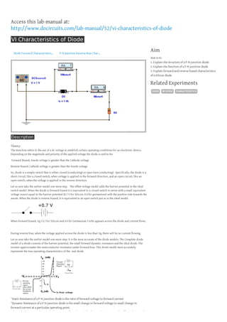
  • 1. Access this lab-manual at: http://www.docircuits.com/lab-manual/52/vi-characteristics-of-diode VI Characteristics of Diode Diode Forward Characteristics... P-N Junction Reverse Bias Char... Aim Aim is to 1. Explain the structure of a P-N junction diode 2. Explain the function of a P-N junction diode 3. Explain forward and reverse biased characteristics of a Silicon diode Related Experiments DIODE Description Theory: The term bias refers to the use of a dc voltage to establish certain operating conditions for an electronic device. Depending on the magnitude and polarity of the applied voltage the diode is said to be: Forward Biased, Anode voltage is greater than the Cathode voltage Reverse Biased, Cathode voltage is greater than the Anode voltage So, diode is a simple switch that is either closed (conducting) or open (non conducting). Specifically, the diode is a short circuit, like a closed switch, when voltage is applied in the forward direction, and an open circuit, like an open switch, when the voltage is applied in the reverse direction. Let us now take the earlier model one more step. The offset voltage model adds the barrier potential to the ideal switch model. When the diode is forward biased it is equivalent to a closed switch in series with a small equivalent voltage source equal to the barrier potential (0.7 V for Silicon, 0.4 for germanium) with the positive side towards the anode. When the diode is reverse biased, it is equivalent to an open switch just as in the ideal model. When forward biased, Vg ( 0.7 for Silicon and 0.4 for Germanium ) volts appears across the diode and current flows. During reverse bias, when the voltage applied across the diode is less than Vg, there will be no current flowing. Let us now take the earlier model one more step. It is the most accurate of the diode models. The Complete diode model of a diode consists of the barrier potential, the small forward dynamic resistance and the ideal diode. The resistor approximates the semiconductor resistance under forward bias. This diode model most accurately represents the true operating characteristics of the real diode. ¨Static Resistance of a P-N junction diode is the ratio of forward voltage to forward current ¨Dynamic Resistance of a P-N junction diode is the small change in forward voltage to small change in forward current at a particular operating point. When a diode is reverse biased a leakage current flows through the device. This current can be effectively ignored REVERSE CHARACTERISTICS
  • 2. When a diode is reverse biased a leakage current flows through the device. This current can be effectively ignored as long as the reverse breakdown voltage of the diode is not exceeded. At potentials greater than the reverse breakdown voltage, charge is pulled through the p-n junction by the strong electric fields in the device and large reverse current flows. This usually destroys the device. There are special diodes that are designed to operate in breakdown. Such diodes are called zener diodes and used as voltage regulators. ¨Take Resistor of 1Kohms ¨Connect to Si Diode. ¨Use Ammeter to measure current and Voltmeter to measure Voltage ¨Setup the circuit as shown ¨One way to measure the VI Characteristics of the diode is the set the DC source at various voltage levels ¨Note the current in the ammeter and voltage in the voltmeter ¨Plot the current against voltage ¨Instead of re-running the experiment at various voltage values from DC source, let us parameterize ¨Click on Simulation Properties – DC Analysis ¨Choose DC Source and Vary the voltage from 0V to 5V to record the voltage and current across the diode ¨Run the experiment ¨On successful run, click on Data Analysis to view the current and the voltage readings ¨Choose to plot against the voltage the current. ¨Edit the properties of the graph to view a closer segment of the plot ¨Select 0.4 V to 1.0 V on the X Axis with interval of 0.01 V ¨On the zoomed graph – measure the ¨Cut off Voltage ¨Static Resistance ¨Dynamic Resistance ¨Hint – to calculate Static and Dynamic Resistances ¨Zoom in the Y axis as well. ¨Dynamic Resistance = Slope of the graph for a particular point Reverse-bias characteristics ¨Setup the circuit as before – but reverse the diode in the circuit so that it is reversed biased. ¨Go through the same steps as before to record the Current and Voltage Readings but the stop voltage should be about 60 V. ¨Note that maximum current flows after about 50 V in the reverse direction.. ¨ Conclusion Thus the forward and reverse bias characteristics of the diode have been verified and plotted.