SlideShare a Scribd company logo
1 of 15
Integration without compromise
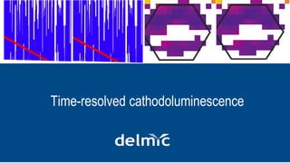
Time-resolved сathodoluminescence
What is time-resolved cathodoluminescence?
• Time-resolved cathodoluminescence is a technique in which
the time dynamics of the cathodoluminescence emission
process is observed
• Main imaging techniques:
1. Lifetime imaging
2. g(2) imaging
How does cathodoluminescence work?
When a sample is bombarded by fast electrons,
the material becomes excited as it returns to a
grounded state, it emits light.
The radiation that is generated in the
ultraviolet/visible/near-infrared regime of the
electromagnetic spectrum is referred to as
cathodoluminescence (CL) as the radiation is
generated by cathode rays (fast electrons).
This data can be collected with nanoscale
resolution and can reveal contrasts that cannot
be observed with any optical microscopy
technique.
Lifetime cathodoluminescence imaging
• Lifetime (or decay trace) mapping is one of the time-resolved techniques
• The method can be used to obtain insight into a large variety of physical
processes and material properties
• To perform lifetime cathodoluminescence imaging, a pulsed electron
microscope is required
Lifetime Imaging Mod
e
Spontaneous light emission process in time
Lifetime Imaging Mod
e
To study lifetime imaging,
a fast photodetector such
as an avalanche
photodiode (APD) or
photomultiplier tube (PMT)
can be used to detect
single photons with high
sensitivity and timing-
precision
Detection
Lifetime Imaging Mod
e
Application of lifetime imaging technique
CL decay-trace measurements can be used for a large range of applications
The extracted lifetime measurements are valuable to obtain information on
intrinsic material properties as well as the local optical environment
Obtaining time dynamics of the material can be very useful for studying
semiconductor materials used for optoelectronic devices or rare-earth doped
materials
Lifetime Imaging Mod
e
Application of lifetime imaging technique
Lifetime Imaging Mod
e
Cathodoluminescence g(2) imaging
• The g(2) function is a useful tool to study cathodoluminescence emission
from a (nano)material
• In a beam of light, the distribution of photons can be described by the
normalized second order autocorrelation function g (2) (𝜏)
g(2) Imaging Mode
Antibunching in cathodoluminescence
A single-photon emitter can only emit one photon at a time and therefore it is impossible t
o observe coincident photons.
When the g(2) function drops below 1 with g(2)(0)= 0, it is referred to as antibunching.
The antibunching effect can be used to identify and characterize quantum sources
of light.
Figure 4: Characteristic g(2) curves for
different cases. The red balls represent a
schematic photon distribution in time for
particular g(2) curves.
g(2) Imaging Mode
g(2) detector
• The most common approach to measure the g(2)(𝜏) is in a Hanbury Brown and Twiss (HBT)
interferometer consisting of a 50/50 beam splitter with two ultrafast single-photon detectors
(SPDs)
• These SPDs generate a single electrical TTL or NIM pulse for every detected photon, which is then registere
d and timed by time-correlator electronics in a time-correlated single-photon scheme (TCSPC)
• The time-resolved module LAB Cube can coupled to the SPARC CL system with fiber coupler
Figure 5: Schematic overview of the DELMIC L
AB Cube system, that can be used for g(2) acqui
sition.
Bunching g(2) curve courtesy of Dr. Sophie Meur
et
(AMOLF, Amsterdam)
g(2) Imaging Mode
Applications of cathodoluminescence g(2) imaging
• g(2) imaging can be used to identify and characterize single-photon emitter at the nanoscale
• The method can be used in fundamental studies on quantum systems and their interaction with
electron beams
• The bunching effect is useful for studying bulk and mesoscopic materials systems including
optoelectronic devices (such as LEDs and solar cells)
Figure 6: Example of g(2) mapping data on InGaN/GaN
nanorods shown in the SEM image (a). (b) The g(2) data
recorded at three colored squares as indicated by the arro
ws in panel (c) which shows SE intensity recorded togethe
r with
the g(2) data set. Maps of (d) lifetime τe, (e) amplitude g(2) (
0)-1 and (f) the probability of excitation γ are also shown. I
f the
data was too noisy to extract these parameters, the pixel
was left white in the map. The contours of the nanorods ar
e
indicated by the black lines.
Figure courtesy of Dr. Sophie Meuret (AMOLF, Amsterdam
) g(2) Imaging Mode
Cathodoluminescence detector SPARC
The SPARC platform
+ High-performance
cathodoluminescence detection system
+ Modular design allows for addition of
different detectors and detection paths
+ High-precision alignment stage gives
unprecedented photon yield and
reliability
+ Time-resolved mode makes new types
of research possible
Time-resolved SPARC module the LAB Cube
The LAB Cube
+ Lifetime imaging and antibunching
module for SPARC
+ Gives insight into intrinsic material
properties
+ Intuitive and easy to use software
integration with remote control
capabilities
+ Overnight acquisitions for more
accurate measurements
+ The LAB Cube is coupled to the SPARC
with an optical fiber, using the Fiber
Coupler Module
DELMIC B.V.
Address: Kanaalweg 4, 2628 EB,
Delft, The Netherlands
Website: www.delmic.com
Telephone: +31 (0)15 744 01 58
Email: info@delmic.com
Please visit Delmic’s website to learn more about time-
resolved cathodoluminescence

More Related Content

What's hot

Sputtering process and its types
Sputtering process and its typesSputtering process and its types
Sputtering process and its typesMuhammadWajid37
 
Quantum dots 1
Quantum dots 1Quantum dots 1
Quantum dots 1Ashraf Ali
 
Preparation Of MXenes (A novel 2D Material)
Preparation Of MXenes (A novel 2D Material) Preparation Of MXenes (A novel 2D Material)
Preparation Of MXenes (A novel 2D Material) rittwikchatterjee
 
Difference b/w electron, neutron and X-ray diffraction and advantages
Difference b/w electron, neutron and X-ray diffraction and advantagesDifference b/w electron, neutron and X-ray diffraction and advantages
Difference b/w electron, neutron and X-ray diffraction and advantagesBHOLU RAM SWAMI
 
X ray diffraction(xrd) principle and use
X ray diffraction(xrd) principle and useX ray diffraction(xrd) principle and use
X ray diffraction(xrd) principle and useSrikumar Swain
 
Transmission Electron Microscope (TEM) for research (Full version)
Transmission Electron Microscope (TEM) for research (Full version)Transmission Electron Microscope (TEM) for research (Full version)
Transmission Electron Microscope (TEM) for research (Full version)Mohit Rajput
 
laser ablation and pyrolysis for micro machining and nano fabrication
laser ablation and pyrolysis for micro machining and nano fabricationlaser ablation and pyrolysis for micro machining and nano fabrication
laser ablation and pyrolysis for micro machining and nano fabricationJAISMON FRANCIS
 
Arc discharge method
Arc discharge methodArc discharge method
Arc discharge methodSudama04
 

What's hot (20)

Sputtering process and its types
Sputtering process and its typesSputtering process and its types
Sputtering process and its types
 
XRD
XRDXRD
XRD
 
X ray diffraction
X ray diffractionX ray diffraction
X ray diffraction
 
Metamaterial
MetamaterialMetamaterial
Metamaterial
 
Mie theory of light scattering
Mie theory of light scatteringMie theory of light scattering
Mie theory of light scattering
 
Quantum dots 1
Quantum dots 1Quantum dots 1
Quantum dots 1
 
Preparation Of MXenes (A novel 2D Material)
Preparation Of MXenes (A novel 2D Material) Preparation Of MXenes (A novel 2D Material)
Preparation Of MXenes (A novel 2D Material)
 
Analytical instrument
Analytical instrumentAnalytical instrument
Analytical instrument
 
Difference b/w electron, neutron and X-ray diffraction and advantages
Difference b/w electron, neutron and X-ray diffraction and advantagesDifference b/w electron, neutron and X-ray diffraction and advantages
Difference b/w electron, neutron and X-ray diffraction and advantages
 
X ray diffraction(xrd) principle and use
X ray diffraction(xrd) principle and useX ray diffraction(xrd) principle and use
X ray diffraction(xrd) principle and use
 
Metamaterials
Metamaterials Metamaterials
Metamaterials
 
X – ray diffraction by iswar hazarika
X – ray diffraction by iswar hazarikaX – ray diffraction by iswar hazarika
X – ray diffraction by iswar hazarika
 
Transmission Electron Microscope (TEM) for research (Full version)
Transmission Electron Microscope (TEM) for research (Full version)Transmission Electron Microscope (TEM) for research (Full version)
Transmission Electron Microscope (TEM) for research (Full version)
 
laser ablation and pyrolysis for micro machining and nano fabrication
laser ablation and pyrolysis for micro machining and nano fabricationlaser ablation and pyrolysis for micro machining and nano fabrication
laser ablation and pyrolysis for micro machining and nano fabrication
 
Basics of-xrd
Basics of-xrdBasics of-xrd
Basics of-xrd
 
X ray diffraction(xrd)
X ray diffraction(xrd)X ray diffraction(xrd)
X ray diffraction(xrd)
 
Arc discharge method
Arc discharge methodArc discharge method
Arc discharge method
 
Superconductivity
Superconductivity Superconductivity
Superconductivity
 
Photoluminescence
PhotoluminescencePhotoluminescence
Photoluminescence
 
Metamaterialsppt
MetamaterialspptMetamaterialsppt
Metamaterialsppt
 

Similar to What is time-resolved cathodoluminescence?

Compendium.imaging.physics
Compendium.imaging.physicsCompendium.imaging.physics
Compendium.imaging.physicspooja joshi
 
Optical Fiber Device For Coupling A Composite-Type Optical Fiber Scope And Pu...
Optical Fiber Device For Coupling A Composite-Type Optical Fiber Scope And Pu...Optical Fiber Device For Coupling A Composite-Type Optical Fiber Scope And Pu...
Optical Fiber Device For Coupling A Composite-Type Optical Fiber Scope And Pu...IJRES Journal
 
DESPECKLING OF SAR IMAGES BY OPTIMIZING AVERAGED POWER SPECTRAL VALUE IN CURV...
DESPECKLING OF SAR IMAGES BY OPTIMIZING AVERAGED POWER SPECTRAL VALUE IN CURV...DESPECKLING OF SAR IMAGES BY OPTIMIZING AVERAGED POWER SPECTRAL VALUE IN CURV...
DESPECKLING OF SAR IMAGES BY OPTIMIZING AVERAGED POWER SPECTRAL VALUE IN CURV...ijistjournal
 
Simulation of AlGaN/Si and InN/Si ELECTRIC –DEVICES
Simulation of AlGaN/Si and InN/Si ELECTRIC –DEVICESSimulation of AlGaN/Si and InN/Si ELECTRIC –DEVICES
Simulation of AlGaN/Si and InN/Si ELECTRIC –DEVICESijrap
 
Simulation of AlGaN/Si and InN/Si ELECTRIC –DEVICES
Simulation of AlGaN/Si and InN/Si ELECTRIC –DEVICESSimulation of AlGaN/Si and InN/Si ELECTRIC –DEVICES
Simulation of AlGaN/Si and InN/Si ELECTRIC –DEVICESijrap
 
Detection of Gamma Radiation
Detection of Gamma RadiationDetection of Gamma Radiation
Detection of Gamma Radiation@Saudi_nmc
 
Simulation Of Algan/Si And Inn/Si Electric - Devices
Simulation Of Algan/Si And Inn/Si Electric - DevicesSimulation Of Algan/Si And Inn/Si Electric - Devices
Simulation Of Algan/Si And Inn/Si Electric - Devicesijrap
 
A tunable telecom wavelength entangled light emitting diode deployed in an in...
A tunable telecom wavelength entangled light emitting diode deployed in an in...A tunable telecom wavelength entangled light emitting diode deployed in an in...
A tunable telecom wavelength entangled light emitting diode deployed in an in...xSo 96O671
 
Jin_single_photon(4)
Jin_single_photon(4)Jin_single_photon(4)
Jin_single_photon(4)Jin Wang
 
Ultrafast response of metal-semiconductor hybrid.pptx
Ultrafast response of metal-semiconductor hybrid.pptxUltrafast response of metal-semiconductor hybrid.pptx
Ultrafast response of metal-semiconductor hybrid.pptxSabinaGurung12
 
JOHN_RAE_1102333_PROJECTREPORT
JOHN_RAE_1102333_PROJECTREPORTJOHN_RAE_1102333_PROJECTREPORT
JOHN_RAE_1102333_PROJECTREPORTJohn Rae
 
Nanoscience MPhys Final Year Research Project Poster Presentation
Nanoscience MPhys Final Year Research Project Poster PresentationNanoscience MPhys Final Year Research Project Poster Presentation
Nanoscience MPhys Final Year Research Project Poster PresentationJakub Lewandowski
 
A Review over Different Blur Detection Techniques in Image Processing
A Review over Different Blur Detection Techniques in Image ProcessingA Review over Different Blur Detection Techniques in Image Processing
A Review over Different Blur Detection Techniques in Image Processingpaperpublications3
 

Similar to What is time-resolved cathodoluminescence? (20)

Compendium.imaging.physics
Compendium.imaging.physicsCompendium.imaging.physics
Compendium.imaging.physics
 
Nonlinear optics
Nonlinear opticsNonlinear optics
Nonlinear optics
 
Pa nalytical pdf
Pa nalytical pdfPa nalytical pdf
Pa nalytical pdf
 
Optical Fiber Device For Coupling A Composite-Type Optical Fiber Scope And Pu...
Optical Fiber Device For Coupling A Composite-Type Optical Fiber Scope And Pu...Optical Fiber Device For Coupling A Composite-Type Optical Fiber Scope And Pu...
Optical Fiber Device For Coupling A Composite-Type Optical Fiber Scope And Pu...
 
DESPECKLING OF SAR IMAGES BY OPTIMIZING AVERAGED POWER SPECTRAL VALUE IN CURV...
DESPECKLING OF SAR IMAGES BY OPTIMIZING AVERAGED POWER SPECTRAL VALUE IN CURV...DESPECKLING OF SAR IMAGES BY OPTIMIZING AVERAGED POWER SPECTRAL VALUE IN CURV...
DESPECKLING OF SAR IMAGES BY OPTIMIZING AVERAGED POWER SPECTRAL VALUE IN CURV...
 
DESPECKLING OF SAR IMAGES BY OPTIMIZING AVERAGED POWER SPECTRAL VALUE IN CURV...
DESPECKLING OF SAR IMAGES BY OPTIMIZING AVERAGED POWER SPECTRAL VALUE IN CURV...DESPECKLING OF SAR IMAGES BY OPTIMIZING AVERAGED POWER SPECTRAL VALUE IN CURV...
DESPECKLING OF SAR IMAGES BY OPTIMIZING AVERAGED POWER SPECTRAL VALUE IN CURV...
 
Simulation of AlGaN/Si and InN/Si ELECTRIC –DEVICES
Simulation of AlGaN/Si and InN/Si ELECTRIC –DEVICESSimulation of AlGaN/Si and InN/Si ELECTRIC –DEVICES
Simulation of AlGaN/Si and InN/Si ELECTRIC –DEVICES
 
Simulation of AlGaN/Si and InN/Si ELECTRIC –DEVICES
Simulation of AlGaN/Si and InN/Si ELECTRIC –DEVICESSimulation of AlGaN/Si and InN/Si ELECTRIC –DEVICES
Simulation of AlGaN/Si and InN/Si ELECTRIC –DEVICES
 
Detection of Gamma Radiation
Detection of Gamma RadiationDetection of Gamma Radiation
Detection of Gamma Radiation
 
Simulation Of Algan/Si And Inn/Si Electric - Devices
Simulation Of Algan/Si And Inn/Si Electric - DevicesSimulation Of Algan/Si And Inn/Si Electric - Devices
Simulation Of Algan/Si And Inn/Si Electric - Devices
 
A tunable telecom wavelength entangled light emitting diode deployed in an in...
A tunable telecom wavelength entangled light emitting diode deployed in an in...A tunable telecom wavelength entangled light emitting diode deployed in an in...
A tunable telecom wavelength entangled light emitting diode deployed in an in...
 
Jin_single_photon(4)
Jin_single_photon(4)Jin_single_photon(4)
Jin_single_photon(4)
 
Ultrafast response of metal-semiconductor hybrid.pptx
Ultrafast response of metal-semiconductor hybrid.pptxUltrafast response of metal-semiconductor hybrid.pptx
Ultrafast response of metal-semiconductor hybrid.pptx
 
Prabhakar singh ii sem-paper v-detection & measurement of radioactivity
Prabhakar singh  ii sem-paper v-detection & measurement of radioactivityPrabhakar singh  ii sem-paper v-detection & measurement of radioactivity
Prabhakar singh ii sem-paper v-detection & measurement of radioactivity
 
JOHN_RAE_1102333_PROJECTREPORT
JOHN_RAE_1102333_PROJECTREPORTJOHN_RAE_1102333_PROJECTREPORT
JOHN_RAE_1102333_PROJECTREPORT
 
HgI2 As X-Ray Imager: Modulation Transfer Function Approach
HgI2 As X-Ray Imager: Modulation Transfer Function Approach HgI2 As X-Ray Imager: Modulation Transfer Function Approach
HgI2 As X-Ray Imager: Modulation Transfer Function Approach
 
Nanoscience MPhys Final Year Research Project Poster Presentation
Nanoscience MPhys Final Year Research Project Poster PresentationNanoscience MPhys Final Year Research Project Poster Presentation
Nanoscience MPhys Final Year Research Project Poster Presentation
 
Ndt
NdtNdt
Ndt
 
X-Ray diffraction Spec methods for analysis
X-Ray diffraction Spec methods for analysisX-Ray diffraction Spec methods for analysis
X-Ray diffraction Spec methods for analysis
 
A Review over Different Blur Detection Techniques in Image Processing
A Review over Different Blur Detection Techniques in Image ProcessingA Review over Different Blur Detection Techniques in Image Processing
A Review over Different Blur Detection Techniques in Image Processing
 

Recently uploaded

Botany 4th semester file By Sumit Kumar yadav.pdf
Botany 4th semester file By Sumit Kumar yadav.pdfBotany 4th semester file By Sumit Kumar yadav.pdf
Botany 4th semester file By Sumit Kumar yadav.pdfSumit Kumar yadav
 
Broad bean, Lima Bean, Jack bean, Ullucus.pptx
Broad bean, Lima Bean, Jack bean, Ullucus.pptxBroad bean, Lima Bean, Jack bean, Ullucus.pptx
Broad bean, Lima Bean, Jack bean, Ullucus.pptxjana861314
 
Chromatin Structure | EUCHROMATIN | HETEROCHROMATIN
Chromatin Structure | EUCHROMATIN | HETEROCHROMATINChromatin Structure | EUCHROMATIN | HETEROCHROMATIN
Chromatin Structure | EUCHROMATIN | HETEROCHROMATINsankalpkumarsahoo174
 
Biological Classification BioHack (3).pdf
Biological Classification BioHack (3).pdfBiological Classification BioHack (3).pdf
Biological Classification BioHack (3).pdfmuntazimhurra
 
TEST BANK For Radiologic Science for Technologists, 12th Edition by Stewart C...
TEST BANK For Radiologic Science for Technologists, 12th Edition by Stewart C...TEST BANK For Radiologic Science for Technologists, 12th Edition by Stewart C...
TEST BANK For Radiologic Science for Technologists, 12th Edition by Stewart C...ssifa0344
 
Natural Polymer Based Nanomaterials
Natural Polymer Based NanomaterialsNatural Polymer Based Nanomaterials
Natural Polymer Based NanomaterialsAArockiyaNisha
 
GBSN - Microbiology (Unit 2)
GBSN - Microbiology (Unit 2)GBSN - Microbiology (Unit 2)
GBSN - Microbiology (Unit 2)Areesha Ahmad
 
All-domain Anomaly Resolution Office U.S. Department of Defense (U) Case: “Eg...
All-domain Anomaly Resolution Office U.S. Department of Defense (U) Case: “Eg...All-domain Anomaly Resolution Office U.S. Department of Defense (U) Case: “Eg...
All-domain Anomaly Resolution Office U.S. Department of Defense (U) Case: “Eg...Sérgio Sacani
 
Orientation, design and principles of polyhouse
Orientation, design and principles of polyhouseOrientation, design and principles of polyhouse
Orientation, design and principles of polyhousejana861314
 
Biopesticide (2).pptx .This slides helps to know the different types of biop...
Biopesticide (2).pptx  .This slides helps to know the different types of biop...Biopesticide (2).pptx  .This slides helps to know the different types of biop...
Biopesticide (2).pptx .This slides helps to know the different types of biop...RohitNehra6
 
Pests of cotton_Borer_Pests_Binomics_Dr.UPR.pdf
Pests of cotton_Borer_Pests_Binomics_Dr.UPR.pdfPests of cotton_Borer_Pests_Binomics_Dr.UPR.pdf
Pests of cotton_Borer_Pests_Binomics_Dr.UPR.pdfPirithiRaju
 
SOLUBLE PATTERN RECOGNITION RECEPTORS.pptx
SOLUBLE PATTERN RECOGNITION RECEPTORS.pptxSOLUBLE PATTERN RECOGNITION RECEPTORS.pptx
SOLUBLE PATTERN RECOGNITION RECEPTORS.pptxkessiyaTpeter
 
Botany 4th semester series (krishna).pdf
Botany 4th semester series (krishna).pdfBotany 4th semester series (krishna).pdf
Botany 4th semester series (krishna).pdfSumit Kumar yadav
 
Nanoparticles synthesis and characterization​ ​
Nanoparticles synthesis and characterization​  ​Nanoparticles synthesis and characterization​  ​
Nanoparticles synthesis and characterization​ ​kaibalyasahoo82800
 
Stunning ➥8448380779▻ Call Girls In Panchshil Enclave Delhi NCR
Stunning ➥8448380779▻ Call Girls In Panchshil Enclave Delhi NCRStunning ➥8448380779▻ Call Girls In Panchshil Enclave Delhi NCR
Stunning ➥8448380779▻ Call Girls In Panchshil Enclave Delhi NCRDelhi Call girls
 
Hire 💕 9907093804 Hooghly Call Girls Service Call Girls Agency
Hire 💕 9907093804 Hooghly Call Girls Service Call Girls AgencyHire 💕 9907093804 Hooghly Call Girls Service Call Girls Agency
Hire 💕 9907093804 Hooghly Call Girls Service Call Girls AgencySheetal Arora
 
STERILITY TESTING OF PHARMACEUTICALS ppt by DR.C.P.PRINCE
STERILITY TESTING OF PHARMACEUTICALS ppt by DR.C.P.PRINCESTERILITY TESTING OF PHARMACEUTICALS ppt by DR.C.P.PRINCE
STERILITY TESTING OF PHARMACEUTICALS ppt by DR.C.P.PRINCEPRINCE C P
 
GBSN - Biochemistry (Unit 1)
GBSN - Biochemistry (Unit 1)GBSN - Biochemistry (Unit 1)
GBSN - Biochemistry (Unit 1)Areesha Ahmad
 

Recently uploaded (20)

Botany 4th semester file By Sumit Kumar yadav.pdf
Botany 4th semester file By Sumit Kumar yadav.pdfBotany 4th semester file By Sumit Kumar yadav.pdf
Botany 4th semester file By Sumit Kumar yadav.pdf
 
Broad bean, Lima Bean, Jack bean, Ullucus.pptx
Broad bean, Lima Bean, Jack bean, Ullucus.pptxBroad bean, Lima Bean, Jack bean, Ullucus.pptx
Broad bean, Lima Bean, Jack bean, Ullucus.pptx
 
Chromatin Structure | EUCHROMATIN | HETEROCHROMATIN
Chromatin Structure | EUCHROMATIN | HETEROCHROMATINChromatin Structure | EUCHROMATIN | HETEROCHROMATIN
Chromatin Structure | EUCHROMATIN | HETEROCHROMATIN
 
CELL -Structural and Functional unit of life.pdf
CELL -Structural and Functional unit of life.pdfCELL -Structural and Functional unit of life.pdf
CELL -Structural and Functional unit of life.pdf
 
Biological Classification BioHack (3).pdf
Biological Classification BioHack (3).pdfBiological Classification BioHack (3).pdf
Biological Classification BioHack (3).pdf
 
TEST BANK For Radiologic Science for Technologists, 12th Edition by Stewart C...
TEST BANK For Radiologic Science for Technologists, 12th Edition by Stewart C...TEST BANK For Radiologic Science for Technologists, 12th Edition by Stewart C...
TEST BANK For Radiologic Science for Technologists, 12th Edition by Stewart C...
 
Natural Polymer Based Nanomaterials
Natural Polymer Based NanomaterialsNatural Polymer Based Nanomaterials
Natural Polymer Based Nanomaterials
 
GBSN - Microbiology (Unit 2)
GBSN - Microbiology (Unit 2)GBSN - Microbiology (Unit 2)
GBSN - Microbiology (Unit 2)
 
All-domain Anomaly Resolution Office U.S. Department of Defense (U) Case: “Eg...
All-domain Anomaly Resolution Office U.S. Department of Defense (U) Case: “Eg...All-domain Anomaly Resolution Office U.S. Department of Defense (U) Case: “Eg...
All-domain Anomaly Resolution Office U.S. Department of Defense (U) Case: “Eg...
 
Orientation, design and principles of polyhouse
Orientation, design and principles of polyhouseOrientation, design and principles of polyhouse
Orientation, design and principles of polyhouse
 
Biopesticide (2).pptx .This slides helps to know the different types of biop...
Biopesticide (2).pptx  .This slides helps to know the different types of biop...Biopesticide (2).pptx  .This slides helps to know the different types of biop...
Biopesticide (2).pptx .This slides helps to know the different types of biop...
 
Pests of cotton_Borer_Pests_Binomics_Dr.UPR.pdf
Pests of cotton_Borer_Pests_Binomics_Dr.UPR.pdfPests of cotton_Borer_Pests_Binomics_Dr.UPR.pdf
Pests of cotton_Borer_Pests_Binomics_Dr.UPR.pdf
 
The Philosophy of Science
The Philosophy of ScienceThe Philosophy of Science
The Philosophy of Science
 
SOLUBLE PATTERN RECOGNITION RECEPTORS.pptx
SOLUBLE PATTERN RECOGNITION RECEPTORS.pptxSOLUBLE PATTERN RECOGNITION RECEPTORS.pptx
SOLUBLE PATTERN RECOGNITION RECEPTORS.pptx
 
Botany 4th semester series (krishna).pdf
Botany 4th semester series (krishna).pdfBotany 4th semester series (krishna).pdf
Botany 4th semester series (krishna).pdf
 
Nanoparticles synthesis and characterization​ ​
Nanoparticles synthesis and characterization​  ​Nanoparticles synthesis and characterization​  ​
Nanoparticles synthesis and characterization​ ​
 
Stunning ➥8448380779▻ Call Girls In Panchshil Enclave Delhi NCR
Stunning ➥8448380779▻ Call Girls In Panchshil Enclave Delhi NCRStunning ➥8448380779▻ Call Girls In Panchshil Enclave Delhi NCR
Stunning ➥8448380779▻ Call Girls In Panchshil Enclave Delhi NCR
 
Hire 💕 9907093804 Hooghly Call Girls Service Call Girls Agency
Hire 💕 9907093804 Hooghly Call Girls Service Call Girls AgencyHire 💕 9907093804 Hooghly Call Girls Service Call Girls Agency
Hire 💕 9907093804 Hooghly Call Girls Service Call Girls Agency
 
STERILITY TESTING OF PHARMACEUTICALS ppt by DR.C.P.PRINCE
STERILITY TESTING OF PHARMACEUTICALS ppt by DR.C.P.PRINCESTERILITY TESTING OF PHARMACEUTICALS ppt by DR.C.P.PRINCE
STERILITY TESTING OF PHARMACEUTICALS ppt by DR.C.P.PRINCE
 
GBSN - Biochemistry (Unit 1)
GBSN - Biochemistry (Unit 1)GBSN - Biochemistry (Unit 1)
GBSN - Biochemistry (Unit 1)
 

What is time-resolved cathodoluminescence?

  • 2. What is time-resolved cathodoluminescence? • Time-resolved cathodoluminescence is a technique in which the time dynamics of the cathodoluminescence emission process is observed • Main imaging techniques: 1. Lifetime imaging 2. g(2) imaging
  • 3. How does cathodoluminescence work? When a sample is bombarded by fast electrons, the material becomes excited as it returns to a grounded state, it emits light. The radiation that is generated in the ultraviolet/visible/near-infrared regime of the electromagnetic spectrum is referred to as cathodoluminescence (CL) as the radiation is generated by cathode rays (fast electrons). This data can be collected with nanoscale resolution and can reveal contrasts that cannot be observed with any optical microscopy technique.
  • 4. Lifetime cathodoluminescence imaging • Lifetime (or decay trace) mapping is one of the time-resolved techniques • The method can be used to obtain insight into a large variety of physical processes and material properties • To perform lifetime cathodoluminescence imaging, a pulsed electron microscope is required Lifetime Imaging Mod e
  • 5. Spontaneous light emission process in time Lifetime Imaging Mod e
  • 6. To study lifetime imaging, a fast photodetector such as an avalanche photodiode (APD) or photomultiplier tube (PMT) can be used to detect single photons with high sensitivity and timing- precision Detection Lifetime Imaging Mod e
  • 7. Application of lifetime imaging technique CL decay-trace measurements can be used for a large range of applications The extracted lifetime measurements are valuable to obtain information on intrinsic material properties as well as the local optical environment Obtaining time dynamics of the material can be very useful for studying semiconductor materials used for optoelectronic devices or rare-earth doped materials Lifetime Imaging Mod e
  • 8. Application of lifetime imaging technique Lifetime Imaging Mod e
  • 9. Cathodoluminescence g(2) imaging • The g(2) function is a useful tool to study cathodoluminescence emission from a (nano)material • In a beam of light, the distribution of photons can be described by the normalized second order autocorrelation function g (2) (𝜏) g(2) Imaging Mode
  • 10. Antibunching in cathodoluminescence A single-photon emitter can only emit one photon at a time and therefore it is impossible t o observe coincident photons. When the g(2) function drops below 1 with g(2)(0)= 0, it is referred to as antibunching. The antibunching effect can be used to identify and characterize quantum sources of light. Figure 4: Characteristic g(2) curves for different cases. The red balls represent a schematic photon distribution in time for particular g(2) curves. g(2) Imaging Mode
  • 11. g(2) detector • The most common approach to measure the g(2)(𝜏) is in a Hanbury Brown and Twiss (HBT) interferometer consisting of a 50/50 beam splitter with two ultrafast single-photon detectors (SPDs) • These SPDs generate a single electrical TTL or NIM pulse for every detected photon, which is then registere d and timed by time-correlator electronics in a time-correlated single-photon scheme (TCSPC) • The time-resolved module LAB Cube can coupled to the SPARC CL system with fiber coupler Figure 5: Schematic overview of the DELMIC L AB Cube system, that can be used for g(2) acqui sition. Bunching g(2) curve courtesy of Dr. Sophie Meur et (AMOLF, Amsterdam) g(2) Imaging Mode
  • 12. Applications of cathodoluminescence g(2) imaging • g(2) imaging can be used to identify and characterize single-photon emitter at the nanoscale • The method can be used in fundamental studies on quantum systems and their interaction with electron beams • The bunching effect is useful for studying bulk and mesoscopic materials systems including optoelectronic devices (such as LEDs and solar cells) Figure 6: Example of g(2) mapping data on InGaN/GaN nanorods shown in the SEM image (a). (b) The g(2) data recorded at three colored squares as indicated by the arro ws in panel (c) which shows SE intensity recorded togethe r with the g(2) data set. Maps of (d) lifetime τe, (e) amplitude g(2) ( 0)-1 and (f) the probability of excitation γ are also shown. I f the data was too noisy to extract these parameters, the pixel was left white in the map. The contours of the nanorods ar e indicated by the black lines. Figure courtesy of Dr. Sophie Meuret (AMOLF, Amsterdam ) g(2) Imaging Mode
  • 13. Cathodoluminescence detector SPARC The SPARC platform + High-performance cathodoluminescence detection system + Modular design allows for addition of different detectors and detection paths + High-precision alignment stage gives unprecedented photon yield and reliability + Time-resolved mode makes new types of research possible
  • 14. Time-resolved SPARC module the LAB Cube The LAB Cube + Lifetime imaging and antibunching module for SPARC + Gives insight into intrinsic material properties + Intuitive and easy to use software integration with remote control capabilities + Overnight acquisitions for more accurate measurements + The LAB Cube is coupled to the SPARC with an optical fiber, using the Fiber Coupler Module
  • 15. DELMIC B.V. Address: Kanaalweg 4, 2628 EB, Delft, The Netherlands Website: www.delmic.com Telephone: +31 (0)15 744 01 58 Email: info@delmic.com Please visit Delmic’s website to learn more about time- resolved cathodoluminescence