![May 9, 2016 2
Processor
Memory
Year
Performance
[instructions/time]
Memory Wall
1980 1990 2000 2010
10
100,000
10,000
1,000
100
1
Beyond von Neumann Architecture
MEMORY
ProcessorMemory
Controller
Processing
Elements](data:image/gif;base64,R0lGODlhAQABAIAAAAAAAP///yH5BAEAAAAALAAAAAABAAEAAAIBRAA7)
Empfohlen
Empfohlen
Weitere ähnliche Inhalte
Ähnlich wie Rotem Ben-Hur,Graduate Student,Technio
Ähnlich wie Rotem Ben-Hur,Graduate Student,Technio (20)
Mehr von chiportal
Mehr von chiportal (20)
Kürzlich hochgeladen
Kürzlich hochgeladen (20)
Rotem Ben-Hur,Graduate Student,Technio
- 1. May 9, 2016 1 Processing within a Memristive Memory Using Memory Processing Unit Rotem Ben-Hur & Shahar Kvatinsky EE, Technion - Israel Institute of Technology
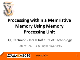
- 2. May 9, 2016 2 Processor Memory Year Performance [instructions/time] Memory Wall 1980 1990 2000 2010 10 100,000 10,000 1,000 100 1 Beyond von Neumann Architecture MEMORY ProcessorMemory Controller Processing Elements
- 3. May 9, 2016 3 MAGIC-NOR within a memristive memory Proposed architecture Synthesis optimization Performance evaluation Outline
- 4. May 9, 2016 4 MAGIC-NOR within a memristive memory Proposed architecture Synthesis optimization Performance evaluation Outline
- 5. May 9, 2016 5 5 NORIN2IN1 100 010 001 011 RON ROFF >> RON ROFF ROFF <<VG Increase resistance >VG/2 ROFF RON RON Initialize OUT to RON S. Kvatinsky, D. Belousov, S. Liman, G. Satat, N. Wald, E. G. Friedman, A. Kolodny, and U. C. Weiser, "MAGIC – Memristor Aided LoGIC," IEEE TCAS II, Nov. 2014 R ON = Logic ‘1’ R OFF = Logic ‘0’ MAGIC-NOR Operation
- 6. May 9, 2016 6 6 VG VG IN IN OUT MAGIC-NOR in a Memristive Memory
- 7. May 9, 2016 7 VG VG IN IN OUT MAGIC-NOR in a Memristive Memory
- 8. May 9, 2016 8 8 N. Talati, S. Gupta, P. Mane, and S. Kvatinsky, “Logic Design within Memristive Memories Using MAGIC," IEEE Trans. on Nanotechnology, 2016 VIsolate VG VG IN IN OUT IN IN OUT VG VG IN IN OUT MAGIC-NOR in a Memristive Memory
- 9. May 9, 2016 9 Logic Operation – A OR B VIsolate Opcode=OR Column vector Destination address: Row=0 Column=4 Source addresses: A: Row=0 Column=0 B: Row=0 Column=1 Vector length: N=3 𝑨 𝒐𝒓 𝑩 = 𝒏𝒐𝒕 𝑨 𝒏𝒐𝒓 𝑩
- 10. May 9, 2016 10 Logic Operation – A OR B VIsolate Opcode=OR Column vector Destination address: Row=0 Column=4 Source addresses: A: Row=0 Column=0 B: Row=0 Column=1 Vector length: N=3 𝑨 𝒐𝒓 𝑩 = 𝒏𝒐𝒕 𝑨 𝒏𝒐𝒓 𝑩 Total: Latency: 3 step Energy: 3*N operations
- 11. May 9, 2016 11 Beyond von Neumann Architecture MEMORY ProcessorMemory Controller
- 12. May 9, 2016 12 MAGIC-NOR within a memristive memory Proposed architecture Synthesis optimization Performance evaluation Outline
- 13. May 9, 2016 13 Traditional Processor & Memory Interface Memory Processor MemoryController Address Data read/write Controller Control Unit Arithmetic/ Logic Unit
- 14. May 9, 2016 14 Memristive Memory Processor MemoryController Control Unit Arithmetic/ Logic Unit Memory Processing Unit (MPU) MPU RowsControl Columns Control MPU’sController
- 15. May 9, 2016 15 Processor Processor & MPU Interface Memristive Memory RowsControl Columns Control MPU’sController MPU
- 16. May 9, 2016 16 Processor & MPU Interface MPU Processor INSTRUCTION ADDRESS DATA WRITE DATA READ NOT MULT INSTRUCTION
- 17. May 9, 2016 17 Processor MPU’s Controller Memristive Memory RowsControl Columns Control MPU’sController MPU
- 18. May 9, 2016 18 MPU’s Controller Block Diagram Memristive Memory Instruction Valid Data Out Finish MPU’s Controller MPU
- 19. May 9, 2016 19 Memristive Memory Conventional Write Operation Instruction Valid Data Out Finish MPU’s Controller MPU
- 20. May 9, 2016 20 Memristive Memory Logic & Arithmetic Operations Instruction Valid Data Out Finish MPU’s Controller MPU
- 21. May 9, 2016 21 MAGIC-NOR within a memristive memory Proposed architecture Synthesis optimization Performance evaluation Outline
- 22. May 9, 2016 22 comp copynot abs nandor mult MAGIC - NOR add sub xor nor and div sqrtpower
- 23. May 9, 2016 23 Optimized Algorithms Energy Time Area
- 24. May 9, 2016 24 Automatic Synthesis Tools ∙ ∙ ∙
- 25. May 9, 2016 25 MPU – Attractive for Data Intensive Applications • Error Correcting Codes (ECC) • Image processing • Graphics • Machine learning • Optimization 25
- 26. May 9, 2016 26 MAGIC-NOR within a memristive memory Proposed architecture Synthesis optimization Performance evaluation Outline
- 27. May 9, 2016 27 Operation on a Vector Total: Latency: 1 step Energy: N operations N=5 𝒏𝒐𝒕 𝒓𝒐𝒘 1 step N operations 𝒏𝒐𝒕(𝒄𝒐𝒍𝟓) 1 step 1 operation 𝒏𝒐𝒕(𝒄𝒐𝒍𝟒) 1 step 1 operation 𝒏𝒐𝒕(𝒄𝒐𝒍𝟑) 1 step 1 operation 𝒏𝒐𝒕(𝒄𝒐𝒍𝟐) 1 step 1 operation 𝒏𝒐𝒕(𝒄𝒐𝒍𝟏) 1 step 1 operation Total: Latency: N steps Energy: N operations
- 28. May 9, 2016 28 Exploiting Both Rows & Columns Parallelism 𝒏𝒐𝒕 𝒓𝒐𝒘𝟒 1 step N operations Total: Latency: M steps Energy: MxN operations N=5 M=4 𝒏𝒐𝒕 𝒓𝒐𝒘𝟑 1 step N operations 𝒏𝒐𝒕 𝒓𝒐𝒘𝟐 1 step N operations 𝒏𝒐𝒕 𝒓𝒐𝒘𝟏 1 step N operations
- 29. May 9, 2016 29 𝒏𝒐𝒕(𝒄𝒐𝒍𝟓) 1 step M operations Total: Latency: N steps Energy: MxN operations N=5 M=4 𝒏𝒐𝒕(𝒄𝒐𝒍𝟒) 1 step M operations 𝒏𝒐𝒕(𝒄𝒐𝒍𝟑) 1 step M operations 𝒏𝒐𝒕(𝒄𝒐𝒍𝟐) 1 step M operations 𝒏𝒐𝒕(𝒄𝒐𝒍𝟏) 1 step M operations Exploiting Both Rows & Columns Parallelism
- 30. May 9, 2016 30 Example – A OR B (MxN Image) 𝑨 𝒐𝒓 𝑩 = 𝒏𝒐𝒕 𝑨 𝒏𝒐𝒓 𝑩 𝑨 𝑩 𝑩 𝑨 + 𝑩 𝑨 + 𝑩 𝒏𝒐𝒕 𝑩 M steps MxN operations 𝒏𝒐𝒕 𝑩 N steps MxN operations 𝑩 𝑨 𝒏𝒐𝒓 𝑩 M steps MxN operations 𝒏𝒐𝒕(𝑨 + 𝑩) N steps MxN operations Total: Latency: 2M+2N steps Energy: 4MxN operations
- 31. May 9, 2016 31 Evaluation of Logic Operations on Images
- 32. May 9, 2016 32 Conclusion • MPU - Novel architecture : combining logic and memory • Up to 4 orders of magnitude improvement in speed and energy
Hinweis der Redaktion
- Today’s computers’ performance are limited by the data transfer between the processor and memory. As can be seen in the graph, there is a huge Processor-Memory Performance Gap. This bottleneck is called the memory wall. A way to “break” this wall is reducing the necessity of the data transfer. This can be achieved by moving some of the computation in memory. How can this be done?? By using memristors!
- Why are memristors such promising candidates for that? Since memristors have both logic capabilities as well as storage capabilities. We’re going to see how to perform logic using memristors, while focusing on the MAGIC logic family. Then we’ll see our proposed architecture, and talk about the challenges while optimizing the in memory calculations.
- In order to perform any kind of computation within the memory, a complete logic family which is performed using the memory cells is required. MAGIC-NOR gate may be performed this way, thus suits us. Let’s see how.
- Unlike standard logic, in memristors the logical state is stored as resistance rather than voltage. Low resistance is considered as logical 1 and high resistance is considered as logical 0. The basic structure consists two memristors as an input <CLICK> and one separate memristor as an output <CLICK>. In order to perform the operation of the gate to a certain input, first we initialize the output memristor to logic 1. Then we apply the same voltage VG on both input memristors. For 00 the voltage on OUT is relatively small and the logic state of it does not change, although there is a state drift. For other input cases, the voltage is around VG/2 which is sufficient for logic state switching and OUT is switched to logic zero.
- MAGIC-NOR from different angle
- While arranged this way, the MAGIC-NOR operation can be performed within a memristive memory
- The input and output of these gates are memory cells, so the computation is performed using the memory cells, and the result is immediately stored inside the memory. As it appears here, it’s possible to perform the same operation to all rows in parallel. This means a single instruction can be done to multiple vectors, thus data. Therefore these computation method is suitable for SIMD (single instruction multiple data). There is a need to isolate unselected rows (rows that are not part of the computation) so an isolate voltage is applied to them.
- As I said, we can perform the same operation to bits from different rows in parallel, thus it’s a column vector operation. For example, if we want to perform OR operation between 2 vectors then: In ? Cycles and ? Operations we perform OR between two vectors. Note that the number of cycles is independent in vector length.
- As I said, we can perform the same operation to bits from different rows in parallel, thus it’s a column vector operation. For example, if we want to perform OR operation between 2 vectors then: In ? Cycles and ? Operations we perform OR between two vectors. Note that the number of steps is independent in vector length.
- As we’ve seen, we can use any memristor in the memory for computations, so we can use different ones for different calculations. Thus it’s possible to perform both storage and processing all over the memory!
- We’ve seen how to perform computations within the memory. But how can we control these calculations, while not changing the basic memory array structure, and also maintain it compatible with existing computing systems?
- In the traditional systems, there is a memory controller within the processor which is responsible for the IF with the memory. It sends read and write commands along with address and data to the memory. In the memory, there is a controller which is responsible for executing these commands.
- In our proposed architecture, a memory processing unit (MPU) replaces the memory. It consists of a memristive memory and CMOS periphery. This is a non-von Neumann architecture where the memory has independent processing capabilities. In MPU, retained data within the memory act as the input of the logical operations and the result of the operation is immediately stored to the memory cells without need to transfer data out of the memory array. How does it work? The MPU’s controller receives commands from the processor, and divides the instructions into a lot of micro-instructions. Then, the controller sends sequences of control signals to the memory in a pipeline. These signals are converted into voltages which are applied on the rows and columns of the memory, thus changing the required memristors states.
- A new interface protocol between the processor and the MPU is required. Let’s examine this IF.
- Same as the standard architecture, the processor sends instructions to the MPU’s controller. This instructions can be conventional read and write commands, but also all kind of logic and arithmetic commands.
- The brain of the MPU is it’s controller. We’ve designed and implemented such a controller in VHDL environment, and we’re waiting for a memristive memory in order to test it in our lab.
- This is the general structure of the MPU’s controller, that we’ve design and implemented. How does it work? An instruction is sent from the processor to the controller, and enters the CPU In block, which interprets it. By the type of the instruction, the CPU In block decides where to send it for further interpretation.
- For example, a conventional write command is sent by the CPU In block to the write block, which sends the required control signals to each row and column of the memory, through the memory mux.
- Logic and arithmetic operations are much more complex. This time, the CPU in block sends the instruction to the arithmetic block. The arithmetic block divides the macro instruction into micro instructions, which are pipelined to the memory, thus maximize the processing efficiency. Complex commands can be divided into tens if not hundreds of micro-instruction, which are also performed in a pipeline. These micro-operations are built on several levels of abstraction where the lower level of abstraction is the basic logical operation (i.e., NOR operation in MAGIC).
- We’ve seen the proposed architecture. Let’s see what algorithms does the MPU’s controller use.
- Based on the MAGIC-NOR operation, we developed efficient algorithms for all kind of logic and arithmetic operations within the memory, while exploiting the memory capabilities.
- What makes them efficient algorithms for memristive memories? The fact they save energy, time, and area, whereas there is a tradeoff between them. How can we achieve that? By using the memristive memories capability which is parallel processing, and also using minimum memristors for each calculation.
- In order to do that efficiently, automatic tools for synthesis should be developed in the future. How will it work? Assembly instructions will be optimized, using the synthesis tools. Then, an optimized list of micro-instructions based on the basic NOR operation will be executed by the MPU’s controller.
- Also, in order to truly benefit from the memristors capabilities, the right applications should be chosen to be performed within the memory. The best applications are data intensive applications, whereas there is an obvious advantage to operations on data which is stored in matrices, such as image processing.
- Let’s see why operations on matrices are much more efficient, in addition to evaluations of the performance of in-memory matrices calculations.
- CPU’s clk rate: 4GHz DDR4 data rate: 400MHz (Memory rate 200MHz) We implemented a complete flow, starting with the instructions received from the processor, and continuing with the controller that sends control signals to a spice-based memristive memory. Using this flow we evaluated our architectures time and energy performance, and compared it with the standard architecture. As you can see, our architecture has the potential to save several orders of magnitude, both in terms of energy and time!
- What did we learn? That combining processing with memory is a promising possibility to significantly improve computers performance and energy consumption, And we discussed a possible novel architecture in order to achieve it.