UNIT-V FMM.HYDRAULIC TURBINE - Construction and working
Arm teaching material
1. 11
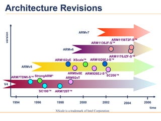
Architecture Revisions
1998 2000 2002 2004
time
version
ARMv5
ARMv6
1994 1996 2006
V4
StrongARM®
ARM926EJ-S™
XScaleTM
ARM102xE ARM1026EJ-S™
ARM9x6E
ARM92xT
ARM1136JF-S™
ARM7TDMI-S™
ARM720T™
XScale is a trademark of Intel Corporation
ARMv7
SC100™
SC200™
ARM1176JZF-S™
ARM1156T2F-S™
2. 22
Data Sizes and Instruction Sets
The ARM is a 32-bit architecture.
When used in relation to the ARM:
Byte means 8 bits
Halfword means 16 bits (two bytes)
Word means 32 bits (four bytes)
Most ARM’s implement two instruction sets
32-bit ARM Instruction Set
16-bit Thumb Instruction Set
Jazelle cores can also execute Java bytecode
3. 33
Processor Modes
The ARM has seven basic operating modes:
User : unprivileged mode under which most tasks run
FIQ : entered when a high priority (fast) interrupt is raised
IRQ : entered when a low priority (normal) interrupt is raised
Supervisor : entered on reset and when a Software Interrupt
instruction is executed
Abort : used to handle memory access violations
Undef : used to handle undefined instructions
System : privileged mode using the same registers as user mode
5. 55
Vector Table
Exception Handling
When an exception occurs, the ARM:
Copies CPSR into SPSR_<mode>
Sets appropriate CPSR bits
Change to ARM state
Change to exception mode
Disable interrupts (if appropriate)
Stores the return address in LR_<mode>
Sets PC to vector address
To return, exception handler needs to:
Restore CPSR from SPSR_<mode>
Restore PC from LR_<mode>
This can only be done in ARM state.
Vector table can be at
0xFFFF0000 on ARM720T
and on ARM9/10 family
devices
FIQ
IRQ
(Reserved)
Data Abort
Prefetch Abort
Software Interrupt
Undefined Instruction
Reset
0x1C
0x18
0x14
0x10
0x0C
0x08
0x04
0x00
6. 6039v12
Program Status Registers
Condition code flags
N = Negative result from ALU
Z = Zero result from ALU
C = ALU operation Carried out
V = ALU operation oVerflowed
Sticky Overflow flag - Q flag
Architecture 5TE/J only
Indicates if saturation has occurred
J bit
Architecture 5TEJ only
J = 1: Processor in Jazelle state
Interrupt Disable bits.
I = 1: Disables the IRQ.
F = 1: Disables the FIQ.
T Bit
Architecture xT only
T = 0: Processor in ARM state
T = 1: Processor in Thumb state
Mode bits
Specify the processor mode
2731
N Z C V Q
28 67
I F T mode
1623 815 5 4 024
f s x c
U n d e f i n e dJ
7. 7039v12
When the processor is executing in ARM state:
All instructions are 32 bits wide
All instructions must be word aligned
Therefore the pc value is stored in bits [31:2] with bits [1:0] undefined (as instruction
cannot be halfword or byte aligned)
When the processor is executing in Thumb state:
All instructions are 16 bits wide
All instructions must be halfword aligned
Therefore the pc value is stored in bits [31:1] with bit [0] undefined (as instruction
cannot be byte aligned)
When the processor is executing in Jazelle state:
All instructions are 8 bits wide
Processor performs a word access to read 4 instructions at once
Program Counter (r15)
8. 88
ARM instructions can be made to execute conditionally by postfixing them with the
appropriate condition code field.
This improves code density and performance by reducing the number of forward
branch instructions.
CMP r3,#0 CMP r3,#0
BEQ skip ADDNE r0,r1,r2
ADD r0,r1,r2
skip
By default, data processing instructions do not affect the condition code flags but
the flags can be optionally set by using “S”. CMP does not need “S”.
loop
…
SUBS r1,r1,#1
BNE loop if Z flag clear then branch
decrement r1 and set flags
Conditional Execution and Flags
9. 99
Condition Codes
Not equal
Unsigned higher or same
Unsigned lower
Minus
Equal
Overflow
No overflow
Unsigned higher
Unsigned lower or same
Positive or Zero
Less than
Greater than
Less than or equal
Always
Greater or equal
EQ
NE
CS/HS
CC/LO
PL
VS
HI
LS
GE
LT
GT
LE
AL
MI
VC
Suffix Description
Z=0
C=1
C=0
Z=1
Flags tested
N=1
N=0
V=1
V=0
C=1 & Z=0
C=0 or Z=1
N=V
N!=V
Z=0 & N=V
Z=1 or N=!V
The possible condition codes are listed below
Note AL is the default and does not need to be specified
10. 1010
Conditional execution examples
if (r0 == 0)
{
r1 = r1 + 1;
}
else
{
r2 = r2 + 1;
}
C source code
5 instructions
5 words
5 or 6 cycles
3 instructions
3 words
3 cycles
CMP r0, #0
BNE else
ADD r1, r1, #1
B end
else
ADD r2, r2, #1
end
...
ARM instructions
unconditional
CMP r0, #0
ADDEQ r1, r1, #1
ADDNE r2, r2, #1
...
conditional
11. 1111
Data Processing Instructions
Consist of :
Arithmetic: ADD ADC SUB SBC RSB RSC
Logical: AND ORR EOR BIC
Comparisons: CMP CMN TST TEQ
Data movement: MOV MVN
These instructions only work on registers, NOT memory.
Syntax:
<Operation>{<cond>}{S} Rd, Rn, Operand2
Comparisons set flags only - they do not specify Rd
Data movement does not specify Rn
Second operand is sent to the ALU via barrel shifter.
12. 1212
Register, optionally with shift operation
Shift value can be either be:
5 bit unsigned integer
Specified in bottom byte of
another register.
Used for multiplication by constant
Immediate value
8 bit number, with a range of 0-
255.
Rotated right through even
number of positions
Allows increased range of 32-bit
constants to be loaded directly
into registers
Result
Operand
1
Barrel
Shifter
Operand
2
ALU
Using a Barrel Shifter:The 2nd Operand
13. 1313
Data Processing Exercise
1. How would you load the two’s complement
representation of -1 into Register 3 using one
instruction?
2. Implement an ABS (absolute value) function for a
registered value using only two instructions.
3. Multiply a number by 35, guaranteeing that it
executes in 2 core clock cycles.
14. 1414
Data Processing Solutions
1. MOVN r6, #0
2. MOVS r7,r7 ; set the flags
RSBMI r7,r7,#0 ; if neg, r7=0-r7
3. ADD r9,r8,r8,LSL #2 ; r9=r8*5
RSB r10,r9,r9,LSL #3 ; r10=r9*7
15. 1515
No ARM instruction can contain a 32 bit immediate constant
All ARM instructions are fixed as 32 bits long
The data processing instruction format has 12 bits available
for operand2
4 bit rotate value (0-15) is multiplied by two to give range 0-
30 in steps of 2
Rule to remember is
“8-bits rotated right by an even number of bit positions”
0711 8
immed_8
Shifter
ROR
rot
x2
Quick Quiz:
0xe3a004ff
MOV r0, #???
Immediate constants
16. 1616
To allow larger constants to be loaded, the assembler offers a pseudo-
instruction:
LDR rd, =const
This will either:
Produce a MOV or MVN instruction to generate the value (if possible).
or
Generate a LDR instruction with a PC-relative address to read the
constant from a literal pool (Constant data area embedded in the
code).
For example
LDR r0,=0xFF => MOV r0,#0xFF
LDR r0,=0x55555555 => LDR r0,[PC,#Imm12]
…
…
DCD 0x55555555
This is the recommended way of loading constants into a register
Loading 32 bit constants
17. 1717
Single register data transfer
LDR STR Word
LDRB STRB Byte
LDRH STRH Halfword
LDRSB Signed byte load
LDRSH Signed halfword load
Memory system must support all access sizes
Syntax:
LDR{<cond>}{<size>} Rd, <address>
STR{<cond>}{<size>} Rd, <address>
e.g. LDREQB
18. 1818
Address accessed
Address accessed by LDR/STR is specified by a base register with an offset
For word and unsigned byte accesses, offset can be:
An unsigned 12-bit immediate value (i.e. 0 - 4095 bytes)
LDR r0, [r1, #8]
A register, optionally shifted by an immediate value
LDR r0, [r1, r2]
LDR r0, [r1, r2, LSL#2]
This can be either added or subtracted from the base register:
LDR r0, [r1, #-8]
LDR r0, [r1, -r2, LSL#2]
For halfword and signed halfword / byte, offset can be:
An unsigned 8 bit immediate value (i.e. 0 - 255 bytes)
A register (unshifted)
Choice of pre-indexed or post-indexed addressing
Choice of whether to update the base pointer (pre-indexed only)
LDR r0, [r1, #-8]!
19. 1919
Load/Store Exercise
Assume an array of 25 words. A compiler associates
y with r1. Assume that the base address for the
array is located in r2. Translate this C
statement/assignment using just three instructions:
array[10] = array[5] + y;
21. 2121
Load and Store Multiples
Syntax:
<LDM|STM>{<cond>}<addressing_mode> Rb{!}, <register list>
4 addressing modes:
LDMIA / STMIA increment after
LDMIB / STMIB increment before
LDMDA / STMDA decrement after
LDMDB / STMDB decrement beforeIA
r1 Increasing
Address
r4
r0
r1
r4
r0
r1
r4
r0 r1
r4
r0
r10
IB DA DB
LDMxx r10, {r0,r1,r4}
STMxx r10, {r0,r1,r4}
Base Register (Rb)
22. 2222
There are 2 classes of multiply - producing 32-bit and 64-bit results
32-bit versions on an ARM7TDMI will execute in 2 - 5 cycles
MUL r0, r1, r2 ; r0 = r1 * r2
MLA r0, r1, r2, r3 ; r0 = (r1 * r2) + r3
64-bit multiply instructions offer both signed and unsigned versions
For these instruction there are 2 destination registers
[U|S]MULL r4, r5, r2, r3 ; r5:r4 = r2 * r3
[U|S]MLAL r4, r5, r2, r3 ; r5:r4 = (r2 * r3) + r5:r4
Most ARM cores do not offer integer divide instructions
Division operations will be performed by C library routines or inline shifts
Multiply and Divide
23. 2323
Branch : B{<cond>} label
Branch with Link : BL{<cond>} subroutine_label
The processor core shifts the offset field left by 2 positions, sign-extends it
and adds it to the PC
± 32 Mbyte range
How to perform longer branches?
2831 24 0
Cond 1 0 1 L Offset
Condition field
Link bit 0 = Branch
1 = Branch with link
232527
Branch instructions
24. 2424
Register Usage
r8
r9/sb
r10/sl
r11
r12
r13/sp
r14/lr
r15/pc
r0
r1
r2
r3
r4
r5
r6
r7Register variables
Must be preserved
Arguments into function
Result(s) from function
otherwise corruptible
(Additional parameters
passed on stack)
Scratch register
(corruptible)
Stack Pointer
Link Register
Program Counter
The compiler has a set of rules known as a
Procedure Call Standard that determine how to
pass parameters to a function (see AAPCS)
CPSR flags may be corrupted by function call.
Assembler code which links with compiled code
must follow the AAPCS at external interfaces
The AAPCS is part of the new ABI for the ARM
Architecture
Register
- Stack base
- Stack limit if software stack checking selected
- R14 can be used as a temporary once value stacked
- SP should always be 8-byte (2 word) aligned
25. 25039v12
ARM Branches and Subroutines
B <label>
PC relative. ±32 Mbyte range.
BL <subroutine>
Stores return address in LR
Returning implemented by restoring the PC from LR
For non-leaf functions, LR will have to be stacked
STMFD sp!,
{regs,lr}
:
BL func2
:
LDMFD sp!,
{regs,pc}
func1 func2
:
:
BL func1
:
:
:
:
:
:
:
MOV pc, lr
26. 2626
PSR access
MRS and MSR allow contents of CPSR / SPSR to be transferred to / from a
general purpose register or take an immediate value
MSR allows the whole status register, or just parts of it to be updated
Interrupts can be enable/disabled and modes changed, by writing to the CPSR
Typically a read/modify/write strategy should be used:
MRS r0,CPSR ; read CPSR into r0
BIC r0,r0,#0x80 ; clear bit 7 to enable IRQ
MSR CPSR_c,r0 ; write modified value to ‘c’ byte only
In User Mode, all bits can be read but only the condition flags (_f) can be modified
f s x c
2731
N Z C V Q
28 67
I F T mode
1623 15 5 4 024
J
10 8919
GE[3:0] E AIT cond_abcde
28. 2828
Pipeline changes for ARM9TDMI
Instruction
Fetch
Shift + ALU Memory
Access
Reg
WriteReg
Read
Reg
Decode
FETCH DECODE EXECUTE MEMORY WRITE
ARM9TDMI
ARM or Thumb
Inst Decode
Reg Select
Reg
Read
Shift ALU
Reg
Write
Thumb→ARM
decompress
ARM decode
Instruction
Fetch
FETCH DECODE EXECUTE
ARM7TDMI
29. 2929
ARM10 vs. ARM11 Pipelines
ARM11
Fetch
1
Fetch
2
Decode Issue
Shift ALU Saturate
Write
back
MAC
1
MAC
2
MAC
3
Address
Data
Cache
1
Data
Cache
2
Shift + ALU
Memory
Access Reg
Write
FETCH DECODE EXECUTE MEMORY WRITE
Reg Read
Multiply
Branch
Prediction
Instruction
Fetch
ISSUE
ARM or
Thumb
Instruction
Decode Multiply
Add
ARM10
32. 32039v12
High Performance
ARM processor
High-bandwidth
on-chip RAM
High
Bandwidth
External
Memory
Interface
DMA
Bus Master
APB
Bridge
Timer
Keypad
UART
PIO
AHB
APB
High Performance
Pipelined
Burst Support
Multiple Bus Masters
Low Power
Non-pipelined
Simple Interface
An Example AMBA System
&lt;number&gt;
Versions mostly refer to the instruction set that the ARM core executes.
The ARM7, which is still the most often used core in a low-power design, executes the version 4T instruction set. Architectural extensions were added for version 5TE to include DSP instructions, such as 16-bit signed MLA instructions, saturation arithmetic, etc. The ARM926EJ-S and ARM1026EJ-S cores are examples of Version 5 architectures. Version 6 added instructions for doing byte manipulations and graphics algorithms more efficiently. The ARM11 family implemented the Version 6 architecture. Version 7 architectures (which include the Cortex family of cores, such as the Cortex A8, Cortex M3 and Cortex R4) extended the functionality by adding things such as Thumb2, low-power features, and more security.
&lt;number&gt;
The cause of confusion here is the term “word” which will mean 16-bits to people with a 16-bit background.
In the ARM world 16-bits is a “halfword” as the architecture is a 32-bit one, whereas “word” means 32-bits.
There are actually three instruction sets in modern ARM cores (such as the version 7 cores – A8, M3, and R4, and even the M1): you have Thumb, Thumb2 and ARM. One core in particular, the M3, executes only Thumb2 code, not ARM. All the instructions are 16 bits.
Java bytecodes are 8-bit instructions designed to be architecture independent. Jazelle transparently executes most bytecodes in hardware and some in highly optimized ARM code. This is due to a tradeoff between hardware complexity (power consumption & silicon area) and speed.
&lt;number&gt;
&lt;number&gt;
This animated slide shows the way that the banking of registers works. On the left the currently visible set of registers are shown for a particular mode.
On the right are the registers that are banked out whilst in that mode.
Each key press will switch mode:
user -&gt; FIQ -&gt;user -&gt; IRQ -&gt; user -&gt;SVC -&gt; User -&gt; Undef -&gt; User -&gt; Abort and then back to user.
The following slide then shows this in a more static way that is more useful for reference
&lt;number&gt;
Green psr bits are only in certain versions of the ARM architecture
ALU status flags (set if &quot;S&quot; bit set, implied in Thumb state).
Sticky overflow flag (Q flag) is set either when
saturation occurs during QADD, QDADD, QSUB or QDSUB, or
the result of SMLAxy or SMLAWx overflows 32-bits
Once flag has been set can not be modified by one of the above instructions and must write to CPSR using MSR instruction to cleared
PSRs split into four 8-bit fields that can be individually written:
Control(c)bits 0-7
Extension(x)bits 8-15Reserved for future use
Status(s)bits 16-23Reserved for future use
Flags(f)bits 24-31
Bits that are reserved for future use should not be modified by current software. Typically, a read-modify-write strategy should be used to update the value of a status register to ensure future compatibility. Note that the T/J bits in the CPSR should never be changed directly by writing to the PSR (use the BX/BXJ instruction to change state instead).
However, in cases where the processor state is known in advance (e.g. on reset, following an interrupt, or some other exception), an immediate value may be written directly into the status registers, to change only specific bits (e.g. to change mode).
New ARM V6 bits now shown.
&lt;number&gt;
Unusual but powerful feature of the ARM instruction set. Other architectures normally only have conditional branches.
Some recently-added ARM instructions (in v5T and v5TE) are not conditional (e.g. v5T BLX offset)
Core compares condition field in instruction against NZCV flags to determine if instruction should be executed.
&lt;number&gt;
Condition codes are simply a way of testing the ALU status flags.
This slide is for reference only.
&lt;number&gt;
&lt;number&gt;
BICbit clear
ORRbit set
ANDbit mask
EORbit invert
Comparisons produce no results - just set condition codes.
CMPlike SUB
CMNlike ADD (subtract of a negative number is the same as add)
TSTlike AND
TEQlike EOR (eor of identical numbers gives result of zero)
Generally single-cycle execution (except write to PC and register-controlled shift). Mention ARM NOP & Thumb NOP.
Explain RSB and RSC which do subtract in other order (e.g. y-x not x-y)
Does not include multiply (separate instr format). No divide - compiler uses run-time library or barrel shifter to perform division.
Can combine “S” bit with conditional execution, e.g.
ADDEQS r0, r1, r2
&lt;number&gt;
&lt;number&gt;
&lt;number&gt;
Literal pools
These are constant data areas embedded in the code at the end of assembler modules, and at other locations if specified by the user using LTORG. Data value must not be executed (will probably be an undefined instruction), assembly programmer must ensure this by placing LTORG at an appropriate location. ARM C compilers will handle placement of literal pools automatically.
&lt;number&gt;
Instruction cycle timing:
STRLDR
7TDMI2 cycles3 cycles
9TDMI1 cycle1 cycle - interlock if used in next cycle
StrongARM11 cycle1 cycle - interlock if used in next cycle
Xscale1 cycle1 cycle - interlock if used in next 2 cycles
Note size specifier comes after condition code.
Link: &lt;address&gt; explained on next slide.
Note that load/store instructions never set condition codes.
&lt;number&gt;
Halfword access and signed halfword/byte accesses were added to the architecture in v4T, this is the reason the offset field is not as flexible as the normal word/byte load/store - not a problem because these accesses are less common.
Link: diagram on next slide
No “!” for post-indexed because post-increment of base register always happens (otherwise the offset field would not be used at all).
&lt;number&gt;
Several aliases for stack usage are allowed for instance:
LDMFD -&gt; LDMIA
STDFD -&gt; STMDB
&lt;number&gt;
We have two basic types of multiply instructions; those that produce a 32 bit result based on the bottom 32 bits of a 64-bit result, and those that produce the full 64 bit result. Now, for each of those, we can do accumulation or not. We do have signed and unsigned versions of the MUL long instructions. And if we are only using the bottom 32 bits of a 64 bit result for the standard MULS, then there is no reason to have signed versions.
ARM7TDMI and ARM9TDMI use 8-bit Booth’s algorithm, which takes 1 cycle for each byte in Rs and terminates when rest of Rs is all zeros or all ones. Most of the cores have early termination based on contents of operand 2. Therefore smaller value if known should be placed in operand 2 if possible. And as you can see from the examples, there is not support for the use of immediates.
Cycle information is general and specific cores. You should refer to a core’s particular TRM for timing information.
The Cortex-M3 does have hardware divide.
&lt;number&gt;
PC-relative to allow position independent code, and allows restricted branch range to jump to nearby addresses.
How to access full 32-bit address space? Can set up LR manually if needed, then load into PC
MOV lr, pc
LDR pc, =dest
ADS linker will automatically generate long branch veneers for branches beyond 32Mb range.
&lt;number&gt;
The compiler has a set of rules that determines a standard for passing parameters between functions. This is know as the ARM Architecture Procedure Call Standard. The AAPCS defines how functions behave from the processors point of view, defining things such as which registers can be corrupted by a function call (r0-r3, and r12), and which registers are non-corruptible over function calls (in other words, registers that must be preserved over function calls). Those would be registers r4 – r11.
If we are using software stack checking, the compiler would use r9 as a stack base and r10 as a stack limit. Stacks grow unchecked by default. With SWSC, either the C library checks that the stack does not override the heap, or the stack is checked against the stack limit. This just depends on the image memory model. And of course as we’ve seen, r13, 14, and 15 are used as the sp, lr, an pc, respectively.
The Application Binary Interface (ABI) for the ARM® Architecture is a collection of all of the standards used in the ARM architecture, some open and some specific to the ARM, anything from the executable image file standards produced by development tools to exception handling standards, to the AMBA spec. You can view the full ARM ABI on our webpages.
This slide shows the way that ARM branch instructions work
It also shows the need to stack the LR (using STM/LDM instructions) when making subroutine calls within subroutines.
&lt;number&gt;
GE: SIMD status bits
E: Controls LD/ST Endianess
A: disable special type of data abort
IT: controls special conditional execution of THUMB2
For MSR operations, we recommend that only the minimum number of fields are written, because future ARM implementations may need to take extra cycles to write specific fields that have recently been allocated and may cause unwanted results; not writing fields you don&apos;t want to change reduces any such extra cycles or unwanted results to a minimum.
&lt;number&gt;
&lt;number&gt;
Pipeline Comparison
The point of this foil is to show that with the ARM7TDMI a lot of work was carried out in the execute stage of the pipeline. Now with ARM9TDMI the execute stage has been split out into three stages to allow greater throughput.
This then means the CPI is about 1.5 compared against 1.9 for ARM7TDMI, and the operating frequency is approximately double for ARM9TDMI over ARM7TDMI on the same fabrication process. Therefore, at least double the processing power is available.
It is possible for the pipeline to interlock. Forwarding paths have been provided to minimise this as much as possible, but they can still occur. By using a bit of consideration when writing code they can almost be eliminated.
&lt;number&gt;
ARM10 - It just illustrates that another stage was added to the ARM9’s pipeline to provide additional time to handle coprocessor instruction decode and handle branch prediction. The Multiplier is now broken up over two stages, execute and memory, since the multiplier is also pipelined.
Note that the ARM9E multiplier is also pipeline (like ARM10) so the upper diagram strictly only applies to the ARM9TDMI.
ARM11 - The processor is a single issue processor, meaning that only one instruction per cycle can be issued from the issue stage to one of the 3 backend pipeline stages.
While the instructions are issued in order they may complete out of order. This will be depend on availability of data, length of execution and memory access times.
&lt;number&gt;
System Design
Overview of some of the hardware and software technologies that ARM has to support the design in of the ARM core into real products.
Also looks at some of the issues involved with memory maps in ARM based systems.
This slides shows a very generic ARM based design, that is actually fairly representative of the designs that we see being done.
On-chip there will be an ARM core (obviously) together with a number of system dependant peripherals. Also required will be some form of interrupt controller which receives interrupts from the peripherals and raised the IRQ or FIQ input to the ARM as appropriate. This interrupt controller may also provide hardware assistance for prioritizing interrupts.
As far as memory is concerned there is likely to be some (cheap) narrow off-chip ROM (or flash) used to boot the system from. There is also likely to be some 16-bit wide RAM used to store most of the runtime data and perhaps some code copied out of the flash. Then on-chip there may well be some 32-bit memory used to store the interrupt handlers and perhaps stacks.
AMBA systems are based around two buses, a high performance system bus and a lower performance peripheral bus.
The high performance bus (AHB) should connect all of the high performance, high bandwidth modules, such as the ARM Processor, any DMA engines, perhaps some fast, 32 bit wide local RAM (or wider to suit the ARM Bus Master being used), an external memory interface, and the interface to the lower performance bus. The number of modules connected here should be kept to a minimum to reduce the bus loading on this high performance bus and allow it to run much faster.
The bulk of the design modules are placed on the lower performance Peripheral Bus (APB). Modules placed here are not accessed as frequently as AHB modules, and as a result of the APB timing, need not consume power (in their APB interfaces) when there is no APB activity. The address and data bus widths on the APB only need to be as wide as required, compared to the AHB where the maximum address and data widths are specified to maximize system performance in this critical area.
So when a design is being partitioned, the main design criteria are
AHBAPB
High PerformanceLow Power
Frequent AccessSimple Interface
Pipelined timingNon-pipelined
We don’t go into multi-layer AHB, AHB Lite or any other AMBA configurations in this presentation.
AHB is aimed at designers using a central multiplexer interconnection scheme.
All Bus Masters drive out address and control signals for the transfer they wish to perform and the Arbiter decides which access is routed to all the slaves.
A central Decoder is used to select which of the slave data and response signals is fed back to the bus masters.
The central multiplexer solution has been adopted in AHB as the preferred interconnect scheme. However the protocol leaves the final choice up to the designer. As we will see later, the turnaround cycles required for tristate buses have not been optimized out to improve performance. AHB is still therefore suitable for any design flow.