AMD World’s First HBM-Powered Product SK Hynix 3D TSV High-Bandwidth Memory 2015 teardown reverse costing report published by Yole Developpement

The first ever 3D IC combining DRAM & GPU with TSV & Silicon Interposer Packaging Analysis & Reverse Costing Report Led by AMD and SK Hynix, this 3D component integrates HBM memories (connected with via-middle TSV and micro-bumps) and GPU stacked onto a silicon interposer (including also via-middle TSV). The report will include a complete physical analysis of the 3D packaging process, with details on all technical choices regarding process and equipment (wafer bonding, via etching, via filling, bumping, underfill…) Also, System Plus Consulting in partnership with Yole Developpement has identified the complete manufacturing supply chain (GPU foundry, Interposer foundry, HBM Foundry, Substrate manufacturer, OSAT) in order to provide a detailed description of the manufacturing process with manufacturing cost calculation. System Plus Consulting will soon release a complete report on the world’s first HBM integrated on chip. Featured in the latest AMD graphic card Radeon™ R9 Fury X, the HBM delivers 60% more memory bandwidth, 3x the performance per watt and consumes 94% less PCB area than GDDR5. More information on that report at http://www.i-micronews.com/reports.html

Recommended
Recommended
More Related Content
More from Yole Developpement
More from Yole Developpement (20)
Recently uploaded
Recently uploaded (20)
AMD World’s First HBM-Powered Product SK Hynix 3D TSV High-Bandwidth Memory 2015 teardown reverse costing report published by Yole Developpement
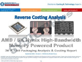
- 1. DISCLAIMER : System Plus Consulting provides cost studies based on its knowledge of the manufacturing and selling prices of electronic components and systems. The given values are realistic estimates which do not bind System Plus Consulting nor the manufacturers quoted in the report. System Plus Consulting is in no case responsible for the consequences related to the use which is made of the contents of this report. The quoted trademarks are property of their owners. © 2015 by SYSTEM PLUS CONSULTING, all rights reserved. 1 Electronic Costing & Technology Experts www.systemplus.fr 21 rue la Nouë Bras de Fer 44200 Nantes – France Phone : +33 (0) 240 180 916 email : info@systemplus.fr September 2015 – Version 1 – Written by Romain Fraux
- 2. AMD High Bandwidth Memory Return to TOC © 2015 by SYSTEM PLUS CONSULTING, all rights reserved. 2 Glossary 1. Overview / Introduction 4 – Executive Summary – Reverse Costing Methodology 2. Company Profile 7 – AMD 3. Physical Analysis 12 – Synthesis of the Physical Analysis – Physical Analysis Methodology – Graphic Card 15 – Graphic Card Opening – Package 18 – View, Dimensions & Marking – Dies Size – HBM Logic & DRAM Dies 22 – View, Dimensions & Marking – µBumps & TSVs – Package Cross-Section 33 – Package Cross-Section – PCB & Frame Cross-Section – Interposer Cross-Section – GPU µBumps Cross-Section – HBM Stack Cross-Section (Side Mold, µBumps, Underfill, TSV) – Comparison with Samsung 3D TSV DRAM Stacking 67 4. Manufacturing Process Flow 70 – Global Overview – GPU Process Description & Foundry – Interposer Process Flow & Foundry – HBM Stack Process Flow (TSV & TCB) & Foundry – Flip-Chip & Stacking Process Flow & Assembly Unit 6. Cost Analysis 94 – Main steps of economic analysis – Yields Hypotheses – GPU Front-End & Die Cost – Interposer Wafer Cost – Interposer Wafer Cost per Process Steps – Interposer Die Cost – HBM Front-End Cost (DRAM + Logic) – HBM TSV Manufacturing Cost – HBM TSV Manufacturing Cost per Process Steps – HBM Micro-Bumping Manufacturing Cost – HBM Micro-Bumping Cost per Process Steps – HBM Dies Cost (DRAM + Logic) – HBM Stack Cost – Final Assembly Manufacturing Cost – Final Assembly Manufacturing Cost per Process Steps – Final Component Cost Contact 120
- 3. AMD High Bandwidth Memory Return to TOC © 2015 by SYSTEM PLUS CONSULTING, all rights reserved. 3 • This full reverse costing study has been conducted to provide insight on technology data, manufacturing cost and selling price of the AMD advanced packaging process used for the Radeon R9 Fury X. • Featured in the latest AMD graphic card Radeon™ R9 Fury X, it is the world’s first HBM integrated on chip. The HBM delivers 60% more memory bandwidth, 3x the performance per watt and consumes 94% less PCB area than GDDR5 according to AMD. • Led by AMD and SK Hynix, this 3D component integrates HBM memories (connected with via- middle TSV and micro-bumps) and GPU stacked onto a silicon interposer (including also via-middle TSV). • The report include a complete physical analysis of the 3D packaging process, with details on all technical choices regarding process and equipment (wafer bonding, via etching, via filling, bumping, underfill…). • Also, it identify the complete manufacturing supply chain (GPU foundry, Interposer foundry, HBM Foundry, Substrate manufacturer, OSAT) in order to provide a detailed description of the manufacturing process with manufacturing cost calculation.
- 4. AMD High Bandwidth Memory Return to TOC © 2015 by SYSTEM PLUS CONSULTING, all rights reserved. 4 • Component Manufacturing Supply Chain:
- 5. AMD High Bandwidth Memory Return to TOC © 2015 by SYSTEM PLUS CONSULTING, all rights reserved. 5 Thermal Paste AMD Radeon Fury X with HBM & GPU
- 6. AMD High Bandwidth Memory Return to TOC © 2015 by SYSTEM PLUS CONSULTING, all rights reserved. 6
- 7. AMD High Bandwidth Memory Return to TOC © 2015 by SYSTEM PLUS CONSULTING, all rights reserved. 7
- 8. AMD High Bandwidth Memory Return to TOC © 2015 by SYSTEM PLUS CONSULTING, all rights reserved. 8 • The dies marking includes the logo of AMD and: 2014 2V5-086203-00 Logic Die Marking
- 9. AMD High Bandwidth Memory Return to TOC © 2015 by SYSTEM PLUS CONSULTING, all rights reserved. 9
- 10. AMD High Bandwidth Memory Return to TOC © 2015 by SYSTEM PLUS CONSULTING, all rights reserved. 10
- 11. AMD High Bandwidth Memory Return to TOC © 2015 by SYSTEM PLUS CONSULTING, all rights reserved. 11
- 12. AMD High Bandwidth Memory Return to TOC © 2015 by SYSTEM PLUS CONSULTING, all rights reserved. 12
- 13. AMD High Bandwidth Memory Return to TOC © 2015 by SYSTEM PLUS CONSULTING, all rights reserved. 13
- 14. AMD High Bandwidth Memory Return to TOC © 2015 by SYSTEM PLUS CONSULTING, all rights reserved. 14
- 15. AMD High Bandwidth Memory Return to TOC © 2015 by SYSTEM PLUS CONSULTING, all rights reserved. 15
- 16. AMD High Bandwidth Memory Return to TOC © 2015 by SYSTEM PLUS CONSULTING, all rights reserved. 16 Reverse costing analysis represents the best cost/price evaluation given the publically available data, and estimates completed by industry experts. Given the hypothesis presented in this analysis, the major sources of correction would lead to a +/- 10% correction on the manufacturing cost (if all parameters are cumulated). These results are open for discussion. We can reevaluate this circuit with your information. Please contact us: o Consulting and Specific Analysis – North America: Steve LaFerriere, Business Development Manager, Yole Inc Email: laferriere@yole.fr – Japan: Yutaka Katano, General Manager, Yole Japan & President, Yole K.K. Email: katano@yole.fr – RoW: Jean-Christophe Eloy, President & CEO, Yole Développement Email: eloy@yole.fr o Report business – North America: Steve LaFerriere, Business Development Manager, Yole Inc Email: laferriere@yole.fr – Europe: Jérôme Azemar, Business Development Manager, European Office Email: azemar@yole.fr – Japan & Asia: Takashi Onozawa, Sales Asia & General Manager, Yole K.K. Email: onozawa@yole.fr – Korea: Hailey Yang, Business Development Manager, Korean Office Email: yang@yole.fr o Financial services – Jean-Christophe Eloy, CEO & President Email: eloy@yole.fr