2. 2
Thermionic (vacuum tube) diodes and solid state (semiconductor) diodes were developed
separately, at approximately the same time, in the early 1900s, as radio receiver detectors.
Until the 1950s vacuum tube diodes were used more frequently in radios because the early
point contact type semiconductor diodes were less stable, also, most receiving sets had
vacuum tubes for amplification that could easily have the thermionic diodes included in the
tube (e.g. 12sQ7 double diode triode) vacuum tube rectifiers and gas filled rectifiers were
capable of handling some high voltage – high current rectification tasks better than the
semiconductor diodes ( such as selenium rectifiers) which were available at the same time.
1873, Fredrick Guthrie discovered the basic principle of operation of thermionic diodes.
Guthrie discovered that a positively charged electroscope could be
discharged by bringing a grounded piece of white-hot metal close to it(but not
actually touching it). The same did not apply to a negatively charged
electroscope, indicating that the current flow was only possible in one
direction.
3. 1 DISCUSS BASIC SEMICONDUCTOR MATERIALS ATOMIC STRUCTURE OF
WHICH DIODES AND TRANSISTORS ARE MADE.
2 THE P – N JUNCTION, P AND N TYPE MATERIALS.
3 APPLICATIONS OF THE DIODE CIRCUITS.
4 DIODE CONDUCTION .
3
Various
diodes
4. As seen in this model, electrons circle the nucleus.
Atomic structure of a material determines it’s ability to conduct
or insulate.
The nucleus is positively charged and has the (+) protons and
neutrons, which is neutral.
Electrons ( - ) are negatively charged and in discrete shells.
The atomic number ( Z ) is the number of protons, and which
determines the particular element.
4
5. ,
The ability of a material to conduct current is based on its atomic structure.
The orbit paths of the electrons surrounding the nucleus are called shells.
Each shell has a defined number of electrons it will hold. This is a fact of nature and
can be determined by the formula 2n2.
The outer shell is called the valence shell.
The less complete a shell is filled to capacity the more conductive the material.
5
6. The valence shell determines the ability of
material to conduct current ( I ).
Silicon atom has 4 electrons in its valence ring.
This makes it a semiconductor.
6
Silicon, 4
electrons in
valence ring
Germanium, 4
electrons in
valence ring
7. There is a forbidden region between the valence band and
ionization level (Conduction Band ).
Since W = QV Equation for WORK done in
moving a charge Q across
potential difference V ( Delta v)
Electron volt 1 eV = (1.6 x 10⁻¹⁹ c ) (1v) = 1.6 10-19 J
Since Eg is less for Germanium (Ge) than Silicon (Si) a larger
number of valence electrons for Ge will have sufficient energy
to cross the forbidden gap and become free. Thus Ge will
have a greater conductivity than Si.
7
8. 8
The four valence electrons are bonded to four adjoining atoms. This
bonding of atoms by sharing of electrons is called covalent bonding. Both are
tetravalent materials, that is both has 4 electrons in their valence ring.
Covalent
bonding of the
silicon or
Germanium
atom
9. Silicon and germanium when carefully refined to reduce impurities to a very
low level, are called intrinsic semiconductors. The conductivity for both pure
materials is quite low.
An increase in temperature causes a substantial increase in the number of
free electrons, thus increasing conductivity.
These materials thus have a negative temperature coefficient of resistance,
( i.e. resistance decreases with temperature).
9
10. There are two types of extrinsic material:
N Type: Impurity atoms have 5 valence electrons
e.g. antimony, arsenic, and phosphorus.
P Type: impurity atoms have 3 valence electrons
e.g. boron, gallium, and indium.
Extrinsic materials is semiconductor materials that has been
subjected to the doping process.
10
12. To be able to use a diode in a circuit, it must be known how it will behave under different voltages and
currents, in other words, the characteristics must be known.
12
Notice the PN junction, depletion region at partial voltage, 0.4 v. and complete collapse
at 0.7v. purple area is resistance in depletion area when diode is 0v or partial
conduction.
VOLTAGE , CURRENT
CHARACTERISTICS OF
DIODES.
13. Graph depicts variation of diode current Id with respect to diode voltage VD is shown,
Observe how current through diode changes (Δ) with respect to voltage.
Initially when forward bias voltage is v0, current Id through diode is also I0 .
The reason , Id through diode is zero (0) because there is no voltage applied across it
terminals which could establish current.
When forward (fv ) bias voltage is gradually increased from zero to threshold voltage,
there is a gradual increase in the value of current.
When forward biased voltage is increased above threshold v, the current increases
very rapidly with respect to voltage. A small change in value of forward biased voltage
would result in large changes in value of forward biased current. As it can be seen on
graph, a small change in forward biased ( Δv) results in drastic change in value of
forward current (Δ I).
Curious to know why there is a sudden rise in the value of current even though the
change in Vd is very small? This is one of the characteristics of diode due to which it is used
in enormous number of applications. The sudden rise in the current can be explained
through the use of solid state physics. The equation concerning behavior of (forward)
current and voltage is given by … Cont’d on 14
13
14. ID = IS (eV
D/ηV
T – 1 ) : This equation is called Shockley’s equation. The term used in the equation
Are as follows:
ID= Current through diode IS = Reverse saturation current η= ideality factor ( H η eta-Greek).
VT is called thermal voltage and is given by VT = KT/q K =Boltzmann’s constant = 1.38 x 10⁻²³ J/K
T = Temperature in Kelvin q= Magnitude of charge on an electron =1.6x10⁻¹⁹ C
Shockley’s equation, which is derived under ideal conditions, suggest that the forward IF rises
exponentially with respect to forward VF. If we expand the right hand side of Shockley’s equation, we get
14
15. 15
When the positive terminal of battery is connected to P – Type material and N – Type
portion to negative terminal, diode is said to be forward biased.
In forward biased state, there is a reduction in net electric field in depletion region and
as a result, electrons can now pass from n-type to p-type semiconductor .
As the magnitude of forward biased is increased, there is an increase in number of
electrons flowing from n-type to p-type material, thus increasing the value of current.
When voltage is increased above threshold v (0.7v), there is a sudden rise in magnitude
of current . ( threshold voltage is defined as voltage above which current increases
very rapidly with respect to voltage).
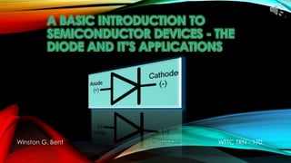
16. The diode is used in a circuit as a one way valve for current ( I ) flow.
A great analogy, would be the one way check valve in a water supply
system. Water can only flow in one direction, blocked in opposite direction.
It is a simple nonlinear (non sequential or straight ) circuit element.
Just like a resistor or other two terminal circuit component, the diode
has two terminals, one terminal on positive side (p-type ) which is called
the anode , the other on negative (n-type ) material and is called the
cathode.
It’s most popular use is in rectifying AC to DC applications.
16
17. The electron theory is best used to describe direction of VF,IF of the forward biased
p-n junction diode. The diode will conduct when a positive source is connected to the
Anode and a negative source connected to the cathode, the voltage and current will
conduct linearly. Silicon conduct at 0.7v and Germanium at 0.3v.
17
One way
valve
18. When donor impurities are introduced into one side and acceptors into the other side of a single crystal semiconductor through
various sophisticated methods of micro-electronic device fabricating methods, a p-n junction is formed.
The p-n junction is a basic structure within semiconconductors. As the name
implies it is a junction between p-type and n-type semiconductor regions.
This structure allows current to flow in one direction thereby providing a
rectification function.
P-type region has an excess of holes while N-type region has an excess of electrons. Where the two regions meet the electrons fill the
holes and there are no free holes or electrons. This means that there are no available charge carriers in the region, it is said to be
depleted, this area is known as the depletion region. Photo shows partial depletion, at full depletion, region collapses completely,
The diode is fully conducting (Forward Biased).
18
Semiconductor p-n
junction depletion
region.
19. If the p-type side is made negative with respect to the
n-type side being made positive, the depletion region
widens until its potential difference equals the biased
voltage, majority carrier current ceases.
19
23. Meade, R.L., & Diffenderfer, R. (2003). Foundations Of Electronics Circuits and Devices. Thomson, NY :
Delmar.
Formation and Properties of Junction Diode, elearnin, https://www.youtube.com.
Diode Introduction For Circuit Analysis, Darryl Morrell. https://www.youtube.com.
Conceptselectronics.com.
23