
Recommended
More Related Content
What's hot
What's hot (20)
Similar to Pin8086
Similar to Pin8086 (20)
More from Mohansonale1
More from Mohansonale1 (6)
Recently uploaded
Recently uploaded (20)
Pin8086
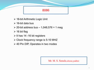
- 1. 16-bit Arithmetic Logic Unit 16-bit data bus 20-bit address bus – 1,048,576 = 1 meg 16 bit flag It has 14 -16 bit registers Clock frequency range is 5-10 MHZ 40 Pin DIP, Operates in two modes 1 8086 Mr. M. S. Sonale,sitcoe,yadrav
- 2. 2 Pin Diagram of 8086
- 3. 3 AD0 - AD15 (I/O): Address Data Bus These lines constitute the time multiplexed memory/IO address during the first clock cycle (T1) and data during T2, T3 and T4 clock cycles. A0 is analogous to BHE for the lower byte of the data bus, pins D0-D7. A0 bit is Low during T1 state when a byte is to be transferred on the lower portion of the bus in memory or I/O operations. 8-bit oriented devices tied to the lower half would normally use A0 to condition chip select functions. These lines are active high and float to tri-state during interrupt acknowledge and local bus "Hold acknowledge". A19/S6, A18/S5, A17/S4, A16/S3 (0): Address/Status During T1 state these lines are the four most significant address lines for memory operations. During I/O operations these lines are low A18/S5 The status of the interrupt enable flag bit is updated at the beginning of each cycle. The status of the flag is indicated through this bus. A19/S6 When Low, it indicates that 8086 is in control of the bus. During a "Hold acknowledge" clock period, the 8086 tri-states the S6 pin and thus allows another bus master to take control of the status bus
- 4. A17/S4 A16/S3 Function 0 0 Extra segment access 0 1 Stack segment access 1 0 Code segment access 1 1 Data segment access After the first clock cycle of an instruction execution, the A17/S4 and A16/S3 pins specify which segment register generates the segment portion of the 8086 address
- 5. During T1 state the BHE should be used to enable data onto the most significant half of the data bus, pins D15 - D8. Eight-bit oriented devices tied to the upper half of the bus would normally use BHE to control chip select functions. 5 BHE /S7 (O): Bus High Enable/Status
- 6. RD (O): READ The Read strobe indicates that the processor is performing a memory or I/O read cycle. This signal is active low during T2 and T3 states. 6
- 7. TEST TEST pin is examined by the "WAIT" instruction. If the TEST pin is Low, execution continues. Otherwise the processor waits in an "idle" state. This input is synchronized internally during each clock cycle on the leading edge of CLK. INTR : Interrupt Request It is a level triggered input which is sampled during the last clock cycle of each instruction to determine if the processor should enter into an interrupt acknowledge operation. A subroutine is vectored to via an interrupt vector look up table located in system memory. It can be internally masked by software resetting the interrupt enable bit INTR is internally synchronized. This signal is active HIGH. NMI : Non-Maskable Interrupt An edge triggered input, causes a type-2 interrupt. A subroutine is vectored to via the interrupt vector look up table located in system memory. NMI is not maskable internally by software. A transition from a LOW to HIGH on this pin initiates the interrupt at the end of the current instruction. This input is internally synchronized Ready Ready is the acknowledgement from the addressed memory or I/O device that it will complete the data transfer. The READY signal from memory or I/O is synchronized by the 8284 clock generator to form READY. This signal is active HIGH. 7
- 8. MN MX: The minimum/maximum mode signal to select the mode of operation either in minimum or maximum mode configuration. Logic 1 indicates minimum mode. M /IO- Memory/IO /M IO signal selects either memory operation or I/O operation. This line indicates that the microprocessor address bus contains either a memory address or an I/O port address. Signal high at this pin indicates a memory operation. INTA- Interrupt acknowledge: The interrupt acknowledge signal is a response to the INTR input signal. The INTAsignal is normally used to gate the interrupt vector number onto the data bus in response to an interrupt request. ALE- Address Latch Enable: This output signal indicates the availability of valid address on the address/data bus, and is connected to latchenable input of latches. DT /R: Data transmit/Receive: This output signal is used to decide the direction of date flow through the bi-directional buffer. DT/R =1 Indicates transmitting and DT/ R=0 indicates receiving the data.
- 9. DEN :- Data Enable: Data bus enable signal indicates the availability of valid data over the address/data lines. 𝑊𝑅 Write: whenever the write signal is at logic 0, the data bus transmits the data tothe memory or I/O devices connected to the system. HOLD: The hold input request a direct memory access(DMA). If the hold signal is at logic 1, this signal is generated by DMA Controller to get memory acess of microprocessor and demands to take control over the address, data and control bus. HLDA :- The HLDA signal is generated by Microprocessor which indicates that the control of memory access of microprocessor and demands to take control over the address, data and control bus is given to DMA controller to perform the remaining operation..
- 10. S2, S1, S0-Status lines: These are the status lines that reflect the type of operation being carried out by the processor. These status lines are encoded as follows S2 S1 S0 Function 0 0 0 Interrupt Acknowledge 0 0 1 Read I/Oport 0 1 0 Write I/Oport 0 1 1 Halt 1 0 0 Code Access 1 0 1 Read memory 1 1 0 Write memory 1 1 1 Passive(In active)
- 11. QS1and QS0-Queue status: The queue status bits shows the status of the internal instruction queue. The encoding of these signals is as follows QS1 QS0 Function 0 0 No operation, queue is idle 0 1 First byte of opcode 1 0 Queue is empty 1 1 Subsequent byte of opcode
- 12. RQ/GT1 and RQ/GT0-request/Grant: The request/grant pins are used by other local bus masters to force the processor to release the local bus at the end of the processors current bus cycle. These lines are bi-directional and are used to both request and grant a DMA operation. RQ/GT0 is having higher priority than RQ/GT1.