
Empfohlen
Weitere ähnliche Inhalte
Ähnlich wie COA.pptx
Ähnlich wie COA.pptx (20)
Kürzlich hochgeladen
Kürzlich hochgeladen (20)
COA.pptx
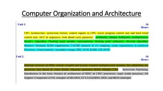
- 1. Computer Organization and Architecture
- 2. UNIT -1 Basic Structure of Computer
- 3. Difference Between Computer Architecture and Computer Organization • Computer Architecture is a functional description of requirements and design implementation for the various parts of a computer. It deals with the functional behavior of computer systems. It comes before the computer organization while designing a computer. • Computer Organization comes after the decision of Computer Architecture first. Computer Organization is how operational attributes are linked together and contribute to realizing the architectural specification. Computer Organization deals with a structural relationship.
- 4. Figure 1: Difference between computer system and computer organization
- 5. S. No. Computer Architecture Computer Organization 1. Architecture describes what the computer does. The Organization describes how it does it. 2. Computer Architecture deals with the functional behavior of computer systems. Computer Organization deals with a structural relationship. 3. In the above figure, it’s clear that it deals with high-level design issues. In the above figure, it’s also clear that it deals with low-level design issues. 4. Architecture indicates its hardware. Where Organization indicates its performance. 5. As a programmer, you can view architecture as a series of instructions, addressing modes, and registers. The implementation of the architecture is called organization. 6. For designing a computer, its architecture is fixed first. For designing a computer, an organization is decided after its architecture. 7. Computer Architecture is also called Instruction Set Architecture (ISA). Computer Organization is frequently called microarchitecture. 8. Computer Architecture comprises logical functions such as instruction sets, registers, data types, and addressing modes. Computer Organization consists of physical units like circuit designs, peripherals, and adders. 9. The different architectural categories found in our computer systems are as follows: 1.Von-Neumann Architecture 2.Harvard Architecture 3.Instruction Set Architecture 4.Micro-architecture 5.System Design CPU organization is classified into three categories based on the number of address fields: 1.Organization of a single Accumulator. 2.Organization of general registers 3.Stack organization 10. It makes the computer’s hardware visible. It offers details on how well the computer performs. 11. Architecture coordinates the hardware and software of the system. Computer Organization handles the segments of the network in a system. 12. The software developer is aware of it. It escapes the software programmer’s detection.
- 6. CPU Architecture/ Functional Unit Figure 2: CPU Architecture
- 7. • Memory holds both data and instructions. • The arithmetic/logic gate unit is capable of performing arithmetic and logic operations on data. • A processor register is a quickly accessible location available to a digital processor's central processing unit (CPU). Registers usually consist of a small amount of fast storage, although some registers have specific hardware functions, and may be read-only or write-only. • The control unit controls the flow of data within the CPU - (which is the Fetch-Execute cycle). • Input arrives into a CPU via a bus. • Output exits the CPU via a bus.
- 8. • Parts of a CPU: ALU - The arithmetic logic unit executes all calculations within the CPU CU - control unit, coordinates how data moves around, decodes instructions • Registers: • a memory location within the actual processor that work at very fast speeds. It stores instructions which await to be decoded or executed. PC - program counter - stores address of the -> next <- instruction in RAM MAR - memory address register - stores the address of the current instruction being executed MDR - memory data register - stores the data that is to be sent to or fetched from memory CIR - current instruction register - stores actual instruction that is being decoded and executed ACC - accumulator - stores result of calculations • Buses: address bus - carries the ADDRESS of the instruction or data data bus - carries data between processor and the memory control bus - sends control signals such as: memory read, memory write Together, these buses may be referred to as the “system bus” or the “front-side bus”
- 15. Figure 3: Hardwired control unit
- 27. Figure 4: Micro-programmed Control Unit
- 30. Instruction Format • A computer will usually have a variety of instruction code format. It is function of control unit within the CPU to interpret each instruction code and provide the necessary control function needed to process the instruction. Syntax:- Opcode Operand
- 31. 1) Opcodes: An operation code field that specifies operation to be performed. Such as add, subtract, complement, shift etc. 2) Operand Address: An address field that designates memory address or processor register. Operations specified by computer instructions are executed on some data stored in memory or processor. operands resides in memory are specified by their memory address. Operands residing in processor register are specified with a register address. I= Mode field The mode field of an instruction specify a variety of alternatives for choosing the operand from the given address. The basic computer has three instruction code format: I Opcode Operand
- 32. 1. Memory reference. 2. Register reference 3. I/O instruction
- 33. 1. Memory reference I Opcode Operand Add In memory reference instruction, if I=0 then it is direct addressing and if I=1 then it is indirect addressing. 2. Register reference I 1 1 1 Register Operation An operand from memory is not needed therefore 12 bits are used to specify operation or test to be executed. 15 14 12 11 0 15 14 12 11 0
- 34. 3. I/O instructions • An I/O instruction does not need reference to memory and is recognized by operation code with a one in the left most bit of an instruction. The remaining 12 bits are used to specify the type of I/O operation or test performed. I 1 1 1 I/O operation 15 14 12 11 0
- 35. Addressing Modes • The different ways in which location of operand is specified in an instruction are referred to as addressing mode. 1) Immediate 2) Direct 3) Indirect 4) Register 5) Register indirect 6) Relative 7) Indexed
- 36. 1. Immediate Addressing • Operand is given explicitly in the instruction. For example ADD 5. this instruction add 5 to the content of accumulator. No memory reference to fetch but in limited range. Format:- Opcode Operand 2. Direct Addressing • In this address field contains address of operand e.g.. ADD A • Effective Address (EA) = Address field of A. This instruction (ADD A) add contents of A to the accumulator. • Look in memory at address A at for operand. • Single memory reference to access data no additional calculation require to calculate effective address. Format:- Memory Opcode Address of A Operand A
- 37. 3. Indirect Addressing • Memory cell pointed by address field and which contains address of operand. • Effective Address (EA) = Address field of A • EA = [A] • E.g. ADD A • Format:- memory • It is Slower Opcode Address Address Operand
- 38. 4. Register Addressing • Operand is present in register named in address field. • Effective Address = R; EA = [R] • Limited number of registers, Very small address field needed. • Shorter instruction, Faster instruction fetch. • No memory access, Fast execution. • Multiple registers help to improve the performance. • Format:- Register Opcode Register Address Operand
- 39. 5. Register Indirect Addressing • Effective address = [R] • Operand is in memory cell pointed by the content of register R. It is having large address space. Fewer memory access than the direct addressing. • Format:- Register memory Opcode Register Add. Address Operand
- 40. 6. Indexed Addressing • Effective address = X+ [R] • Address field holds two values i.e., X= Constant value (offset) R= Register that holds address of memory location. Format:- Register Memory Opcode Register R Const. value Address Operand +
- 41. 7. Relative Addressing • It is a version of displacement address. Where X is address part of the instruction. • Effective Address = X + PC • PC = Program Counter • Get the operand from X byte away from current location pointed by PC.
- 42. Types of Instructions • Computers may have instructions of several different addresses. The no. of address field in the instruction format of a computer depends on internal organization of its registers. Main 3 organizations are as follows: 1. Single Accumulator Organization. 2. General Register Organization. 3. Stack Organization.
- 43. 1. Single Accumulator Organization • In this type of organization that specifies the arithmetic addition is by an assembly language instruction as ADD X, where X is address of operand. The ADD instruction in this case, result in the operation. AC AC+M (x) ADD X
- 44. 2. General Register Organization • The instruction format in this type of computer needs 3 register address field. Thus, instruction for an arithmetic addition may be written as. ADD R1, R2, R3 R1 R2 + R3
- 45. 3. Stack Organization • The stack organization CPU uses stack which uses PUSH and POP operation. These defined operation requires the address field. For eg. PUSH X POP X For the above organization. There are 4 types of instructions-
- 46. Types of Instructions 1. Three Address Instruction 2. Two Address Instruction 3. One Address Instruction 4. Zero Address Instruction
- 47. 1. Three Address Instruction • Computers with three address instruction format can use each address field to specify either a processor register or a memory operand. • The program in assembly language that evaluate X= (A+B)*(C+D) as follows: ADD R1, A, B = R1 M [A] + M [B] ADD R2, C, D = R2 M [C] + M [D] Mul X, R1, R2 = M[X] R1 * R2 It is assumed that the computer has two processor register. The symbol M[A] denotes the operand at memory address symbolized by A. • The advantage of three address format is that it results in short program when evaluating arithmetic operations. The disadvantage is that the binary coded instruction require to many bits to specify three address.
- 48. 2. Two Address Instruction • Two address instruction is most common in commercial system. Here, again, each address field can specify either the processor register or a memory word. The program to evaluate X= (A+B)*(C+D) as follows: Mov R1, A = R1 M [A] ADD R1, B = R1 R1 + M [B] Mov R2, C = R2 M [C] ADD R2, D = R2 R2 + M [D] MUL R1, R2 = R1 R1 * R2 MOV X, R1 = M[X] R1
- 49. 3. One Address Instruction • One address instruction uses an accumulator register for all data manipulation for the purpose of multiplication and division. There is a need for second register and assume that the AC contains the result of all operation. The program is to evaluate: X= (A+B)*(C+D) in one address instruction:- LOAD A AC M[A] ADD B AC AC + M[B] STORE T M[T] AC LOAD C AC M[C] ADD D AC AC + M[D] MUL T AC AC * M[T] STORE X M[X] AC
- 50. 4. Zero Address Instruction • Step organized computes and do not use an address field for the instruction addition and multiplication. • The PUSH and POP instructions however need an address field to specify the operand that communicate with the stack. • The program to evaluate the same operation in Zero address instructions as follows:- PUSH A TOS A PUSH B TOS B ADD TOS A+B PUSH C TOS C PUSH D TOS D ADD TOS C+D MUL TOS (A+B) * (C+D) POP X M[X] TOS
- 51. Look ahead carry generator • The adder produce carry propagation delay while performing other arithmetic operations like multiplication and divisions as it uses several additions or subtraction steps. This is a major problem for the adder and hence improving the speed of addition will improve the speed of all other arithmetic operations. Hence reducing the carry propagation delay (Propagation delay is the amount of time required for a signal to be received after it has been sent; it is caused by the time it takes for the signal to travel through a medium.) of adders is of great importance. • There are different logic design approaches that have been employed to overcome the carry propagation problem. • Like, ripple carry adder, carry look-ahead adder etc. • One widely used approach is to employ a carry look-ahead which solves this problem by calculating the carry signals in advance, based on the input signals. This type of adder circuit is called a carry look-ahead adder. Here a carry signal will be generated in two cases: 1. Input bits A and B are 1, 2. When one of the two bits is 1 and the carry-in is 1.
- 52. • In ripple carry adders, for each adder block, the two bits that are to be added are available instantly. However, each adder block waits for the carry to arrive from its previous block. So, it is not possible to generate the sum and carry of any block until the input carry is known. The block waits for the block to produce its carry. So there will be a considerable time delay which is carry propagation delay. Ripple Carry Adders Figure 5: Ripple Carry Adder
- 53. • Consider the above 4-bit ripple carry adder. The sum is produced by the corresponding full adder as soon as the input signals are applied to it. But the carry input is not available on its final steady-state value until carry is available at its steady-state value. Therefore, though the carry must propagate to all the stages in order that output and carry settle their final steady-state value. The propagation time is equal to the propagation delay of each adder block, multiplied by the number of adder blocks in the circuit. • For example, if each 3 full adder stage has a propagation delay of 20 nanoseconds, then will reach its final correct value after 60 (20 × 3) nanoseconds. The situation gets worse, if we extend the number of stages for adding more number of bits.
- 54. If you are asked to calculate the time after which the output sum bit or carry bit becomes available from any particular full adder, then it is calculated as- • Time After Which Carry Bit Cx Becomes Available- • Required time = Total number of full adders till full adder producing Cx X Carry propagation delay of full adder. • Time After Which Sum Bit Sx Becomes Available- • Required time = Time taken for its carry in to become available + Sum propagation delay of full adder = { Total number of full adders before full adder producing Sx X Carry propagation delay of full adder } + Sum propagation delay of full adder
- 55. Problem-01: • A 16-bit ripple carry adder is realized using 16 identical full adders. The carry propagation delay of each full adder is 12 ns and the sum propagation delay of each full adder is 15 ns. The worst case delay of this 16 bit adder will be ______? A) 195 ns B) 220 ns C) 250 ns D) 300 ns
- 56. We consider the last full adder for worst case delay. Time after which output carry bit becomes available from the last full adder = Total number of full adders X Carry propagation delay of full adder = 16 x 12 ns = 192 ns Time after which output sum bit becomes available from the last full adder = Time taken for its carry in to become available + Sum propagation delay of full adder = { Total number of full adders before last full adder X Carry propagation delay of full adder } + Sum propagation delay of full adder = { 15 x 12 ns } + 15 ns = 195 ns
- 57. Carry Look-ahead Adder : • A carry look-ahead adder reduces the propagation delay by introducing more complex hardware. In this design, the ripple carry design is suitably transformed such that the carry logic over fixed groups of bits of the adder is reduced to two-level logic. Let us discuss the design in detail. Figure 6: Carry Look-ahead Adder
- 58. • Consider the full adder circuit shown above with corresponding truth table. We define two variables as ‘carry generate’ Gi and ‘carry propagate’ Pi then,
- 59. Figure 7: Look-ahead Carry Generator
- 60. Advantages and Disadvantages of Carry Look-Ahead Adder : Advantages – • The propagation delay is reduced. • It provides the fastest addition logic. Disadvantages – • The Carry Look-ahead adder circuit gets complicated as the number of variables increase. • The circuit is costlier as it involves more number of hardware.
- 61. Question 1.
- 64. Question 2.
- 65. Question 3.
- 67. Question 4.
- 72. Question 5.
- 73. Solution:
- 74. Question 6.