SlideShare ist ein Scribd-Unternehmen logo
1 von 26
INTRODUCTION TO
SEMICONDUCTOR
MATERIALS AND DEVICES
Presented By
S.ARUNBHAARAT
6017f17de69b11e9b0fe59835bdf11f2(App
SASTRA Deemed To be University
B.Tech ECE
1
ACKNOWLEDGEMENT
In preparation of my assignment, I had to take the help and guidance
of some respected persons. As the completion of this assignment
gave me much pleasure, I would like to show my gratitude DR.AJAY
SEMALTY, Course Instructor, from ACADEMIC WRITING under UGC
SWAYAM ONLINE COURSE for giving me a good guidelines for
assignment throughout numerous consultations. I would also like to
expand my gratitude to all those who have directly and indirectly
guided me in writing this assignment.
2
DISCOVERY
Vacuum Tubes- First Generation
Contained Heavy Coverage of tubes in Solid state Era.
Many Engineers joined together and discovered First Transistor on
1950
Miniaturisation limited by three factors
1.Quality
2. Network design
3. Manufacturing Equipment.
3
WHY SEMICONDUCTOR
SELECTED??
4
WHY SEMICONDUCTOR
SELECTED??
Semiconductors have a unique atomic structure that allows their conductivity to be controlled by
stimulation with electric currents, electromagnetic fields, or even light.
Therefore ,Semiconductors and semiconductor devices are the building blocks of all the electronic
devices.
Semiconductor materials generally have conductivity between metals and insulators.
Types of semiconductors
(i) Elemental semiconductors: Si and Ge
(ii) Compound semiconductors :
 Inorganic: CdS, GaAs, CdSe, InP, etc.
 Organic: Anthracene, doped pthalocyanines, etc.
 Organic polymers: Polypyrrole, polyaniline,
polythiophene, etc.
5
BAND THEORY
Isolated atoms of materials have well defined energy levels over which
electrons are distributed (in different orbits)
In crystalline form, when the atoms are closely spaced their outer energy
levels join together to form two separate bands called Valance band and
Conduction band
The energy gap between the valance band and the conduction band is
known as Forbidden energy gap( Eg) or Energy band gap or simply Energy
gap
The conductivity of materials depends on this energy gap. 6
ENERGY BAND STRUCTURE
7
ENERGY BAND STRUCTURE
Metals SemiconductorNon-Metals
8
INTRINSIC SEMICONDUCTORS
An intrinsic semiconductor behaves like an insulator at T = 0 K
It is the thermal energy at higher temperatures (T > 0K), which excites some
electrons from the valence band to the conduction band
9
EXTRINSIC SEMICONDUCTOR
To improve the conductivity the pure Semiconductors are added with small
amounts of Trivalent (Gallium, indium) or Pentavalent (Arsenic, Phosphorous)
impurities
Doping:
Adding small amounts of trivalent or pentavalent impurities to pure
semiconductors to improve their conductivity is known as doping
The Two types of extrinsic semiconductors are:
n-Type semiconductor &
p-Type semiconductor
10
N-TYPE SEMICONDUCTOR
Pure semiconductors doped with small amounts of pentavalent impurities
are known as n-type semiconductors
The four valance electrons of each impurity atom form covalent bond with
the neighboring semiconductor atoms.
The fifth unpaired electron will remain at an energy level much higher than
the bound electrons
This energy level is known as the donor energy level
The donor energy level is very close to conduction band( 0.01 to 0.05 eV).
This electrons can easily jump in to conduction band to become free
electrons by absorbing thermal energy
11
N-TYPE SEMICONDUCTOR
12
P-TYPE SEMICONDUCTORS
In this case the three valance electrons of each trivalent impurity atom forms
covalent bonds with the neighboring semiconductor atom
the fourth neighboring atom will have an unoccupied energy state.
This energy state is called acceptor energy level
Accepter energy level is very close to valance band ( 0.01 to 0.05 ev)
Electrons from valance band can easily jump in to Acceptor energy level
This creates Holes in the valance band
the number holes the valance band is greater than the free electrons in the
conduction band. nh > ne
Majority current carriers in p-type semiconductors are holes
Again ne x nh = ni
2
13
P-TYPE SEMICONDUCTOR
14
P-N JUNCTION (SEMICONDUCTOR
DIODE)
p-n junction is the basic building block of many semiconductor devices like
diodes, transistor, etc
P-type & n-Type semiconductors are fused together to make p-n Junction or
Diode
(a). Diffusion and Drift
In n-type- semiconductor concentration of electrons (number of electrons
per unit volume) is more than the concentration of holes
In a p-type semiconductor, concentration of holes is more than the
concentration of free electrons
During the formation of p-n junction holes diffuse from p-side to n-side (p
→ n) and electrons diffuse from n-side to p-side (n → p)
15
P-N JUNCTION (SEMICONDUCTOR
DIODE)
This motion of charge carries gives rise to diffusion current across the
junction
Due to this diffusion of current carriers, a layer of negative charge (negative
space-charge region) on the p-side and a layer of positive charge (or
positive space-charge region) on n-side of the junction are developed.
This region at the junction free of current carriers is known as Depletion
layer
16
P-N JUNCTION (SEMICONDUCTOR
DIODE)
This diffusion of majority current leads to a layer of +ve charge on n side
and –ve charge on p side
This charge accumulation on either side near the junction produces an
electric field with in the depletion layer from n side to p side, known as
Barrier electric field (Eb)
Due to this electric field electrons move from p side to n side and holes from
n side to p side
This motion of charges due to barrier electric field is known as Drift
That is drift current is opposite to diffusion current
At equilibrium state,
drift current = diffusion current.
17
P-N JUNCTION (SEMICONDUCTOR
DIODE)
Due to the barrier, electric field n side will be at a higher potential compared
to the p side. This potential difference across the depletion layer is called
barrier potential ( V0)
18
P-N JUNCTION DIODE UNDER FORWARD
BIAS
19
P-N JUNCTION DIODE UNDER
FORWARD BIAS
P side is connected to positive & n side is connected to negative
External potential V appears across the depletion layer
Due to the affect of external potential free electrons and holes accumulate in
the depletion layer
Thickness of depletion layer decreases
Free electrons diffuse towards the positive end and holes diffuse to the
negative end setting up a diffusion current( of the range of a few mA)
The current through the diode remains small at the beginning
As external voltage increases, at a particular voltage the current starts
increase rapidly
20
P-N JUNCTION ( DIODE)
FORWARD BIAS
His voltage is known as Thresh hold voltage or Cut in Voltage ( 0.2 V for Ge
& 0.7 Volt for Si).
Beyond thresh hold voltage the diode acts as a good conductor and V-I
relationship is more or less linear
21
REVERSE BIAS
CHARACTERISTICS
P side is connected to negative & n side to positive of the external power
The barrier potential increases as the external voltage.
Depletion layer thickens (widens).
The diode remains non-conducting except for a small drift current (of the
order of a few microampere)
On further increasing, the external voltage the diode breaks down with a
sudden increase in current. This damages the diode. This voltage is known
as break down voltage
A semiconductor Diode(p-n Junction) allows current only in one direction(
Forward Bias).
This property of Diode is used in the construction of a rectifier
22
REVERSE BIAS
CHARACTERISTICS
A semiconductor Diode(p-n Junction) allows current only in one direction(
Forward Bias).
This property of Diode is used in the construction of a rectifier
23
TIPS TO LEARN PHYSICS
NCERT BOOK was only Reference and Text Book
NCERT Worked Out Examples
NCERT Book Back Exercise (Except Additional Exercise)
Previous Yr. Paper
Reference books:
1. XAM Idea (Board Type)
2. S.L..Arora (Board & Entrance exam)
24
REFERENCE
Textbook:
1.NCERT Physics Class 12 Volume 2
2. Electronic Devices and Circuit Theory-By ROBERT BOYLESTAD &
LOUIS NASHELSKY
Website:
1. https://ethw.org/Semiconductors
2.https://www.worldscientific.com/worldscibooks/10.1142/P647
25
26

Weitere ähnliche Inhalte

Was ist angesagt?

A BASIC INTRODUCTION TO SEMICONDUCTOR DEVICES - THE
A BASIC INTRODUCTION TO SEMICONDUCTOR DEVICES - THEA BASIC INTRODUCTION TO SEMICONDUCTOR DEVICES - THE
A BASIC INTRODUCTION TO SEMICONDUCTOR DEVICES - THEWinston Bent A.S.S.
 
Transistor as a switch
Transistor as a switchTransistor as a switch
Transistor as a switchOmed Diyari
 
Pn junction diode by sarmad baloch
Pn junction diode by sarmad balochPn junction diode by sarmad baloch
Pn junction diode by sarmad balochSarmad Baloch
 
Band theory of solids
Band theory of solidsBand theory of solids
Band theory of solidsutpal sarkar
 
Diodes
DiodesDiodes
Diodescallr
 
Metal semiconductor contacts
Metal semiconductor contactsMetal semiconductor contacts
Metal semiconductor contactsKasif Nabi
 
Semiconductors
SemiconductorsSemiconductors
SemiconductorsA B Shinde
 
Class 12th Solids and semiconductor devices part 1
Class 12th Solids and semiconductor devices part 1Class 12th Solids and semiconductor devices part 1
Class 12th Solids and semiconductor devices part 1Arpit Meena
 
Zener Diode Presentation
Zener Diode PresentationZener Diode Presentation
Zener Diode PresentationPritom Mojumder
 
Semiconductor Diode: Introduction and Application
Semiconductor Diode: Introduction and ApplicationSemiconductor Diode: Introduction and Application
Semiconductor Diode: Introduction and ApplicationSamir Raj Bhandari
 

Was ist angesagt? (20)

A BASIC INTRODUCTION TO SEMICONDUCTOR DEVICES - THE
A BASIC INTRODUCTION TO SEMICONDUCTOR DEVICES - THEA BASIC INTRODUCTION TO SEMICONDUCTOR DEVICES - THE
A BASIC INTRODUCTION TO SEMICONDUCTOR DEVICES - THE
 
Transistor as a switch
Transistor as a switchTransistor as a switch
Transistor as a switch
 
Pn junction diode by sarmad baloch
Pn junction diode by sarmad balochPn junction diode by sarmad baloch
Pn junction diode by sarmad baloch
 
Band theory of solids
Band theory of solidsBand theory of solids
Band theory of solids
 
Unit 2 semiconductors
Unit 2  semiconductors Unit 2  semiconductors
Unit 2 semiconductors
 
Tunnel Diode
Tunnel DiodeTunnel Diode
Tunnel Diode
 
Diodes
DiodesDiodes
Diodes
 
Metal semiconductor contacts
Metal semiconductor contactsMetal semiconductor contacts
Metal semiconductor contacts
 
Diode
DiodeDiode
Diode
 
Field Effect Transistor
Field Effect TransistorField Effect Transistor
Field Effect Transistor
 
Semiconductor diode
Semiconductor diodeSemiconductor diode
Semiconductor diode
 
Electrostatics
ElectrostaticsElectrostatics
Electrostatics
 
Semiconductors
SemiconductorsSemiconductors
Semiconductors
 
Tunneling
TunnelingTunneling
Tunneling
 
Diodes
DiodesDiodes
Diodes
 
Class 12th Solids and semiconductor devices part 1
Class 12th Solids and semiconductor devices part 1Class 12th Solids and semiconductor devices part 1
Class 12th Solids and semiconductor devices part 1
 
Intro To Capacitors
Intro To CapacitorsIntro To Capacitors
Intro To Capacitors
 
Tunnel diode
Tunnel diodeTunnel diode
Tunnel diode
 
Zener Diode Presentation
Zener Diode PresentationZener Diode Presentation
Zener Diode Presentation
 
Semiconductor Diode: Introduction and Application
Semiconductor Diode: Introduction and ApplicationSemiconductor Diode: Introduction and Application
Semiconductor Diode: Introduction and Application
 

Ähnlich wie Introduction to Semiconductor Materials and devices

Class 12 th semiconductor part 3
Class 12 th semiconductor part 3Class 12 th semiconductor part 3
Class 12 th semiconductor part 3Priyanka Jakhar
 
Semiconductors summary
Semiconductors summarySemiconductors summary
Semiconductors summaryradebethapi
 
Semiconductors summary
Semiconductors summarySemiconductors summary
Semiconductors summaryradebethapi
 
Semiconductors summary
Semiconductors summarySemiconductors summary
Semiconductors summaryradebethapi
 
Semiconductors summary
Semiconductors summarySemiconductors summary
Semiconductors summaryradebethapi
 
Semiconductor Diodes and Circuits
Semiconductor Diodes and CircuitsSemiconductor Diodes and Circuits
Semiconductor Diodes and CircuitsDarwin Nesakumar
 
EC8353 EDC unit1
EC8353 EDC unit1EC8353 EDC unit1
EC8353 EDC unit1elakkia8
 
227 sample chapter
227 sample chapter227 sample chapter
227 sample chapterAnkit Dubey
 
Pn junction diode class 12 investegatory project
Pn junction diode class 12 investegatory projectPn junction diode class 12 investegatory project
Pn junction diode class 12 investegatory projectabhijeet singh
 
BEEIE UNIT IV PPT.ppt
BEEIE UNIT IV PPT.pptBEEIE UNIT IV PPT.ppt
BEEIE UNIT IV PPT.pptDEEBIKAR2
 
pn junction and zener diode 12 class project.ppt
pn junction and zener diode 12 class project.pptpn junction and zener diode 12 class project.ppt
pn junction and zener diode 12 class project.pptshivam soni
 
Physics Project for class 12 isc Junction and diode
Physics Project for class 12 isc Junction and diodePhysics Project for class 12 isc Junction and diode
Physics Project for class 12 isc Junction and diodeIshani gupta Gupta
 

Ähnlich wie Introduction to Semiconductor Materials and devices (20)

BEEE.pptx
BEEE.pptxBEEE.pptx
BEEE.pptx
 
Semiconductor diodes
Semiconductor diodesSemiconductor diodes
Semiconductor diodes
 
Vivalab
VivalabVivalab
Vivalab
 
Class 12 th semiconductor part 3
Class 12 th semiconductor part 3Class 12 th semiconductor part 3
Class 12 th semiconductor part 3
 
Semiconductors summary
Semiconductors summarySemiconductors summary
Semiconductors summary
 
Semiconductors summary
Semiconductors summarySemiconductors summary
Semiconductors summary
 
Semiconductors summary
Semiconductors summarySemiconductors summary
Semiconductors summary
 
Semiconductors summary
Semiconductors summarySemiconductors summary
Semiconductors summary
 
Semiconductor Diodes and Circuits
Semiconductor Diodes and CircuitsSemiconductor Diodes and Circuits
Semiconductor Diodes and Circuits
 
Theory of solids
Theory of solidsTheory of solids
Theory of solids
 
EC8353 EDC unit1
EC8353 EDC unit1EC8353 EDC unit1
EC8353 EDC unit1
 
Semiconductors
SemiconductorsSemiconductors
Semiconductors
 
227 sample chapter
227 sample chapter227 sample chapter
227 sample chapter
 
Pn junction diode class 12 investegatory project
Pn junction diode class 12 investegatory projectPn junction diode class 12 investegatory project
Pn junction diode class 12 investegatory project
 
Electronics.pptx
Electronics.pptxElectronics.pptx
Electronics.pptx
 
BEEIE UNIT IV PPT.ppt
BEEIE UNIT IV PPT.pptBEEIE UNIT IV PPT.ppt
BEEIE UNIT IV PPT.ppt
 
PN JUNCTION VIVA- VOCE
PN JUNCTION VIVA- VOCEPN JUNCTION VIVA- VOCE
PN JUNCTION VIVA- VOCE
 
pn junction and zener diode 12 class project.ppt
pn junction and zener diode 12 class project.pptpn junction and zener diode 12 class project.ppt
pn junction and zener diode 12 class project.ppt
 
Physics Project for class 12 isc Junction and diode
Physics Project for class 12 isc Junction and diodePhysics Project for class 12 isc Junction and diode
Physics Project for class 12 isc Junction and diode
 
AE UNIT I.ppt
AE UNIT I.pptAE UNIT I.ppt
AE UNIT I.ppt
 

Kürzlich hochgeladen

ESP 4-EDITED.pdfmmcncncncmcmmnmnmncnmncmnnjvnnv
ESP 4-EDITED.pdfmmcncncncmcmmnmnmncnmncmnnjvnnvESP 4-EDITED.pdfmmcncncncmcmmnmnmncnmncmnnjvnnv
ESP 4-EDITED.pdfmmcncncncmcmmnmnmncnmncmnnjvnnvRicaMaeCastro1
 
How to Make a Duplicate of Your Odoo 17 Database
How to Make a Duplicate of Your Odoo 17 DatabaseHow to Make a Duplicate of Your Odoo 17 Database
How to Make a Duplicate of Your Odoo 17 DatabaseCeline George
 
Q-Factor HISPOL Quiz-6th April 2024, Quiz Club NITW
Q-Factor HISPOL Quiz-6th April 2024, Quiz Club NITWQ-Factor HISPOL Quiz-6th April 2024, Quiz Club NITW
Q-Factor HISPOL Quiz-6th April 2024, Quiz Club NITWQuiz Club NITW
 
Blowin' in the Wind of Caste_ Bob Dylan's Song as a Catalyst for Social Justi...
Blowin' in the Wind of Caste_ Bob Dylan's Song as a Catalyst for Social Justi...Blowin' in the Wind of Caste_ Bob Dylan's Song as a Catalyst for Social Justi...
Blowin' in the Wind of Caste_ Bob Dylan's Song as a Catalyst for Social Justi...DhatriParmar
 
Q4-PPT-Music9_Lesson-1-Romantic-Opera.pptx
Q4-PPT-Music9_Lesson-1-Romantic-Opera.pptxQ4-PPT-Music9_Lesson-1-Romantic-Opera.pptx
Q4-PPT-Music9_Lesson-1-Romantic-Opera.pptxlancelewisportillo
 
MS4 level being good citizen -imperative- (1) (1).pdf
MS4 level   being good citizen -imperative- (1) (1).pdfMS4 level   being good citizen -imperative- (1) (1).pdf
MS4 level being good citizen -imperative- (1) (1).pdfMr Bounab Samir
 
Narcotic and Non Narcotic Analgesic..pdf
Narcotic and Non Narcotic Analgesic..pdfNarcotic and Non Narcotic Analgesic..pdf
Narcotic and Non Narcotic Analgesic..pdfPrerana Jadhav
 
ClimART Action | eTwinning Project
ClimART Action    |    eTwinning ProjectClimART Action    |    eTwinning Project
ClimART Action | eTwinning Projectjordimapav
 
Beauty Amidst the Bytes_ Unearthing Unexpected Advantages of the Digital Wast...
Beauty Amidst the Bytes_ Unearthing Unexpected Advantages of the Digital Wast...Beauty Amidst the Bytes_ Unearthing Unexpected Advantages of the Digital Wast...
Beauty Amidst the Bytes_ Unearthing Unexpected Advantages of the Digital Wast...DhatriParmar
 
4.11.24 Mass Incarceration and the New Jim Crow.pptx
4.11.24 Mass Incarceration and the New Jim Crow.pptx4.11.24 Mass Incarceration and the New Jim Crow.pptx
4.11.24 Mass Incarceration and the New Jim Crow.pptxmary850239
 
How to Manage Buy 3 Get 1 Free in Odoo 17
How to Manage Buy 3 Get 1 Free in Odoo 17How to Manage Buy 3 Get 1 Free in Odoo 17
How to Manage Buy 3 Get 1 Free in Odoo 17Celine George
 
4.9.24 School Desegregation in Boston.pptx
4.9.24 School Desegregation in Boston.pptx4.9.24 School Desegregation in Boston.pptx
4.9.24 School Desegregation in Boston.pptxmary850239
 
Oppenheimer Film Discussion for Philosophy and Film
Oppenheimer Film Discussion for Philosophy and FilmOppenheimer Film Discussion for Philosophy and Film
Oppenheimer Film Discussion for Philosophy and FilmStan Meyer
 
Tree View Decoration Attribute in the Odoo 17
Tree View Decoration Attribute in the Odoo 17Tree View Decoration Attribute in the Odoo 17
Tree View Decoration Attribute in the Odoo 17Celine George
 
Unraveling Hypertext_ Analyzing Postmodern Elements in Literature.pptx
Unraveling Hypertext_ Analyzing  Postmodern Elements in  Literature.pptxUnraveling Hypertext_ Analyzing  Postmodern Elements in  Literature.pptx
Unraveling Hypertext_ Analyzing Postmodern Elements in Literature.pptxDhatriParmar
 
Mythology Quiz-4th April 2024, Quiz Club NITW
Mythology Quiz-4th April 2024, Quiz Club NITWMythology Quiz-4th April 2024, Quiz Club NITW
Mythology Quiz-4th April 2024, Quiz Club NITWQuiz Club NITW
 
Concurrency Control in Database Management system
Concurrency Control in Database Management systemConcurrency Control in Database Management system
Concurrency Control in Database Management systemChristalin Nelson
 

Kürzlich hochgeladen (20)

ESP 4-EDITED.pdfmmcncncncmcmmnmnmncnmncmnnjvnnv
ESP 4-EDITED.pdfmmcncncncmcmmnmnmncnmncmnnjvnnvESP 4-EDITED.pdfmmcncncncmcmmnmnmncnmncmnnjvnnv
ESP 4-EDITED.pdfmmcncncncmcmmnmnmncnmncmnnjvnnv
 
How to Make a Duplicate of Your Odoo 17 Database
How to Make a Duplicate of Your Odoo 17 DatabaseHow to Make a Duplicate of Your Odoo 17 Database
How to Make a Duplicate of Your Odoo 17 Database
 
Q-Factor HISPOL Quiz-6th April 2024, Quiz Club NITW
Q-Factor HISPOL Quiz-6th April 2024, Quiz Club NITWQ-Factor HISPOL Quiz-6th April 2024, Quiz Club NITW
Q-Factor HISPOL Quiz-6th April 2024, Quiz Club NITW
 
Blowin' in the Wind of Caste_ Bob Dylan's Song as a Catalyst for Social Justi...
Blowin' in the Wind of Caste_ Bob Dylan's Song as a Catalyst for Social Justi...Blowin' in the Wind of Caste_ Bob Dylan's Song as a Catalyst for Social Justi...
Blowin' in the Wind of Caste_ Bob Dylan's Song as a Catalyst for Social Justi...
 
Q4-PPT-Music9_Lesson-1-Romantic-Opera.pptx
Q4-PPT-Music9_Lesson-1-Romantic-Opera.pptxQ4-PPT-Music9_Lesson-1-Romantic-Opera.pptx
Q4-PPT-Music9_Lesson-1-Romantic-Opera.pptx
 
MS4 level being good citizen -imperative- (1) (1).pdf
MS4 level   being good citizen -imperative- (1) (1).pdfMS4 level   being good citizen -imperative- (1) (1).pdf
MS4 level being good citizen -imperative- (1) (1).pdf
 
Narcotic and Non Narcotic Analgesic..pdf
Narcotic and Non Narcotic Analgesic..pdfNarcotic and Non Narcotic Analgesic..pdf
Narcotic and Non Narcotic Analgesic..pdf
 
ClimART Action | eTwinning Project
ClimART Action    |    eTwinning ProjectClimART Action    |    eTwinning Project
ClimART Action | eTwinning Project
 
Beauty Amidst the Bytes_ Unearthing Unexpected Advantages of the Digital Wast...
Beauty Amidst the Bytes_ Unearthing Unexpected Advantages of the Digital Wast...Beauty Amidst the Bytes_ Unearthing Unexpected Advantages of the Digital Wast...
Beauty Amidst the Bytes_ Unearthing Unexpected Advantages of the Digital Wast...
 
prashanth updated resume 2024 for Teaching Profession
prashanth updated resume 2024 for Teaching Professionprashanth updated resume 2024 for Teaching Profession
prashanth updated resume 2024 for Teaching Profession
 
4.11.24 Mass Incarceration and the New Jim Crow.pptx
4.11.24 Mass Incarceration and the New Jim Crow.pptx4.11.24 Mass Incarceration and the New Jim Crow.pptx
4.11.24 Mass Incarceration and the New Jim Crow.pptx
 
Faculty Profile prashantha K EEE dept Sri Sairam college of Engineering
Faculty Profile prashantha K EEE dept Sri Sairam college of EngineeringFaculty Profile prashantha K EEE dept Sri Sairam college of Engineering
Faculty Profile prashantha K EEE dept Sri Sairam college of Engineering
 
How to Manage Buy 3 Get 1 Free in Odoo 17
How to Manage Buy 3 Get 1 Free in Odoo 17How to Manage Buy 3 Get 1 Free in Odoo 17
How to Manage Buy 3 Get 1 Free in Odoo 17
 
4.9.24 School Desegregation in Boston.pptx
4.9.24 School Desegregation in Boston.pptx4.9.24 School Desegregation in Boston.pptx
4.9.24 School Desegregation in Boston.pptx
 
Mattingly "AI & Prompt Design: Large Language Models"
Mattingly "AI & Prompt Design: Large Language Models"Mattingly "AI & Prompt Design: Large Language Models"
Mattingly "AI & Prompt Design: Large Language Models"
 
Oppenheimer Film Discussion for Philosophy and Film
Oppenheimer Film Discussion for Philosophy and FilmOppenheimer Film Discussion for Philosophy and Film
Oppenheimer Film Discussion for Philosophy and Film
 
Tree View Decoration Attribute in the Odoo 17
Tree View Decoration Attribute in the Odoo 17Tree View Decoration Attribute in the Odoo 17
Tree View Decoration Attribute in the Odoo 17
 
Unraveling Hypertext_ Analyzing Postmodern Elements in Literature.pptx
Unraveling Hypertext_ Analyzing  Postmodern Elements in  Literature.pptxUnraveling Hypertext_ Analyzing  Postmodern Elements in  Literature.pptx
Unraveling Hypertext_ Analyzing Postmodern Elements in Literature.pptx
 
Mythology Quiz-4th April 2024, Quiz Club NITW
Mythology Quiz-4th April 2024, Quiz Club NITWMythology Quiz-4th April 2024, Quiz Club NITW
Mythology Quiz-4th April 2024, Quiz Club NITW
 
Concurrency Control in Database Management system
Concurrency Control in Database Management systemConcurrency Control in Database Management system
Concurrency Control in Database Management system
 

Introduction to Semiconductor Materials and devices

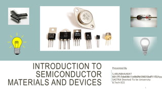
  • 1. INTRODUCTION TO SEMICONDUCTOR MATERIALS AND DEVICES Presented By S.ARUNBHAARAT 6017f17de69b11e9b0fe59835bdf11f2(App SASTRA Deemed To be University B.Tech ECE 1
  • 2. ACKNOWLEDGEMENT In preparation of my assignment, I had to take the help and guidance of some respected persons. As the completion of this assignment gave me much pleasure, I would like to show my gratitude DR.AJAY SEMALTY, Course Instructor, from ACADEMIC WRITING under UGC SWAYAM ONLINE COURSE for giving me a good guidelines for assignment throughout numerous consultations. I would also like to expand my gratitude to all those who have directly and indirectly guided me in writing this assignment. 2
  • 3. DISCOVERY Vacuum Tubes- First Generation Contained Heavy Coverage of tubes in Solid state Era. Many Engineers joined together and discovered First Transistor on 1950 Miniaturisation limited by three factors 1.Quality 2. Network design 3. Manufacturing Equipment. 3
  • 5. WHY SEMICONDUCTOR SELECTED?? Semiconductors have a unique atomic structure that allows their conductivity to be controlled by stimulation with electric currents, electromagnetic fields, or even light. Therefore ,Semiconductors and semiconductor devices are the building blocks of all the electronic devices. Semiconductor materials generally have conductivity between metals and insulators. Types of semiconductors (i) Elemental semiconductors: Si and Ge (ii) Compound semiconductors :  Inorganic: CdS, GaAs, CdSe, InP, etc.  Organic: Anthracene, doped pthalocyanines, etc.  Organic polymers: Polypyrrole, polyaniline, polythiophene, etc. 5
  • 6. BAND THEORY Isolated atoms of materials have well defined energy levels over which electrons are distributed (in different orbits) In crystalline form, when the atoms are closely spaced their outer energy levels join together to form two separate bands called Valance band and Conduction band The energy gap between the valance band and the conduction band is known as Forbidden energy gap( Eg) or Energy band gap or simply Energy gap The conductivity of materials depends on this energy gap. 6
  • 8. ENERGY BAND STRUCTURE Metals SemiconductorNon-Metals 8
  • 9. INTRINSIC SEMICONDUCTORS An intrinsic semiconductor behaves like an insulator at T = 0 K It is the thermal energy at higher temperatures (T > 0K), which excites some electrons from the valence band to the conduction band 9
  • 10. EXTRINSIC SEMICONDUCTOR To improve the conductivity the pure Semiconductors are added with small amounts of Trivalent (Gallium, indium) or Pentavalent (Arsenic, Phosphorous) impurities Doping: Adding small amounts of trivalent or pentavalent impurities to pure semiconductors to improve their conductivity is known as doping The Two types of extrinsic semiconductors are: n-Type semiconductor & p-Type semiconductor 10
  • 11. N-TYPE SEMICONDUCTOR Pure semiconductors doped with small amounts of pentavalent impurities are known as n-type semiconductors The four valance electrons of each impurity atom form covalent bond with the neighboring semiconductor atoms. The fifth unpaired electron will remain at an energy level much higher than the bound electrons This energy level is known as the donor energy level The donor energy level is very close to conduction band( 0.01 to 0.05 eV). This electrons can easily jump in to conduction band to become free electrons by absorbing thermal energy 11
  • 13. P-TYPE SEMICONDUCTORS In this case the three valance electrons of each trivalent impurity atom forms covalent bonds with the neighboring semiconductor atom the fourth neighboring atom will have an unoccupied energy state. This energy state is called acceptor energy level Accepter energy level is very close to valance band ( 0.01 to 0.05 ev) Electrons from valance band can easily jump in to Acceptor energy level This creates Holes in the valance band the number holes the valance band is greater than the free electrons in the conduction band. nh > ne Majority current carriers in p-type semiconductors are holes Again ne x nh = ni 2 13
  • 15. P-N JUNCTION (SEMICONDUCTOR DIODE) p-n junction is the basic building block of many semiconductor devices like diodes, transistor, etc P-type & n-Type semiconductors are fused together to make p-n Junction or Diode (a). Diffusion and Drift In n-type- semiconductor concentration of electrons (number of electrons per unit volume) is more than the concentration of holes In a p-type semiconductor, concentration of holes is more than the concentration of free electrons During the formation of p-n junction holes diffuse from p-side to n-side (p → n) and electrons diffuse from n-side to p-side (n → p) 15
  • 16. P-N JUNCTION (SEMICONDUCTOR DIODE) This motion of charge carries gives rise to diffusion current across the junction Due to this diffusion of current carriers, a layer of negative charge (negative space-charge region) on the p-side and a layer of positive charge (or positive space-charge region) on n-side of the junction are developed. This region at the junction free of current carriers is known as Depletion layer 16
  • 17. P-N JUNCTION (SEMICONDUCTOR DIODE) This diffusion of majority current leads to a layer of +ve charge on n side and –ve charge on p side This charge accumulation on either side near the junction produces an electric field with in the depletion layer from n side to p side, known as Barrier electric field (Eb) Due to this electric field electrons move from p side to n side and holes from n side to p side This motion of charges due to barrier electric field is known as Drift That is drift current is opposite to diffusion current At equilibrium state, drift current = diffusion current. 17
  • 18. P-N JUNCTION (SEMICONDUCTOR DIODE) Due to the barrier, electric field n side will be at a higher potential compared to the p side. This potential difference across the depletion layer is called barrier potential ( V0) 18
  • 19. P-N JUNCTION DIODE UNDER FORWARD BIAS 19
  • 20. P-N JUNCTION DIODE UNDER FORWARD BIAS P side is connected to positive & n side is connected to negative External potential V appears across the depletion layer Due to the affect of external potential free electrons and holes accumulate in the depletion layer Thickness of depletion layer decreases Free electrons diffuse towards the positive end and holes diffuse to the negative end setting up a diffusion current( of the range of a few mA) The current through the diode remains small at the beginning As external voltage increases, at a particular voltage the current starts increase rapidly 20
  • 21. P-N JUNCTION ( DIODE) FORWARD BIAS His voltage is known as Thresh hold voltage or Cut in Voltage ( 0.2 V for Ge & 0.7 Volt for Si). Beyond thresh hold voltage the diode acts as a good conductor and V-I relationship is more or less linear 21
  • 22. REVERSE BIAS CHARACTERISTICS P side is connected to negative & n side to positive of the external power The barrier potential increases as the external voltage. Depletion layer thickens (widens). The diode remains non-conducting except for a small drift current (of the order of a few microampere) On further increasing, the external voltage the diode breaks down with a sudden increase in current. This damages the diode. This voltage is known as break down voltage A semiconductor Diode(p-n Junction) allows current only in one direction( Forward Bias). This property of Diode is used in the construction of a rectifier 22
  • 23. REVERSE BIAS CHARACTERISTICS A semiconductor Diode(p-n Junction) allows current only in one direction( Forward Bias). This property of Diode is used in the construction of a rectifier 23
  • 24. TIPS TO LEARN PHYSICS NCERT BOOK was only Reference and Text Book NCERT Worked Out Examples NCERT Book Back Exercise (Except Additional Exercise) Previous Yr. Paper Reference books: 1. XAM Idea (Board Type) 2. S.L..Arora (Board & Entrance exam) 24
  • 25. REFERENCE Textbook: 1.NCERT Physics Class 12 Volume 2 2. Electronic Devices and Circuit Theory-By ROBERT BOYLESTAD & LOUIS NASHELSKY Website: 1. https://ethw.org/Semiconductors 2.https://www.worldscientific.com/worldscibooks/10.1142/P647 25
  • 26. 26