
Recommended
Recommended
More Related Content
What's hot
What's hot (20)
Similar to High Voltage Darlington Transistor Arrays Datasheet
Similar to High Voltage Darlington Transistor Arrays Datasheet (20)
More from AUTHELECTRONIC
More from AUTHELECTRONIC (20)
Recently uploaded
Recently uploaded (20)
High Voltage Darlington Transistor Arrays Datasheet
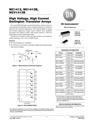
- 1. © Semiconductor Components Industries, LLC, 2006 July, 2006 − Rev. 8 1 Publication Order Number: MC1413/D MC1413, MC1413B, NCV1413B High Voltage, High Current Darlington Transistor Arrays The seven NPN Darlington connected transistors in these arrays are well suited for driving lamps, relays, or printer hammers in a variety of industrial and consumer applications. Their high breakdown voltage and internal suppression diodes insure freedom from problems associated with inductive loads. Peak inrush currents to 500 mA permit them to drive incandescent lamps. The MC1413, B with a 2.7 kW series input resistor is well suited for systems utilizing a 5.0 V TTL or CMOS Logic. Features • Pb−Free Packages are Available* • NCV Prefix for Automotive and Other Applications Requiring Site and Control Changes Figure 1. Representative Schematic Diagram 5.0 k 3.0 k Pin 9 1/7 MC1413, B 2.7 k Figure 2. PIN CONNECTIONS 9 10 11 12 13 14 15 16 8 7 6 5 4 3 2 1 (Top View) *For additional information on our Pb−Free strategy and soldering details, please download the ON Semiconductor Soldering and Mounting Techniques Reference Manual, SOLDERRM/D. http://onsemi.com PDIP−16 P SUFFIX CASE 648 1 16 1 16 SOIC−16 D SUFFIX CASE 751B Device Package Shipping† ORDERING INFORMATION MC1413D SOIC−16 48 Units/Rail MC1413DR2 SOIC−16 2500 Tape & Reel See general marking information in the device marking section on page 5 of this data sheet. DEVICE MARKING INFORMATION MC1413P PDIP−16 25 Units/Rail MC1413BD SOIC−16 48 Units/Rail MC1413BDR2 SOIC−16 2500 Tape & Reel MC1413BP PDIP−16 25 Units/Rail NCV1413BDR2 SOIC−16 2500 Tape & Reel MC1413PG PDIP−16 (Pb−Free) 25 Units/Rail MC1413BDR2G SOIC−16 (Pb−Free) 2500 Tape & Reel †For information on tape and reel specifications, including part orientation and tape sizes, please refer to our Tape and Reel Packaging Specifications Brochure, BRD8011/D. MC1413DR2G SOIC−16 (Pb−Free) 2500 Tape & Reel MC1413DG SOIC−16 (Pb−Free) 48 Units/Tube MC1413BDG SOIC−16 (Pb−Free) 48 Units/Rail MC1413BPG PDIP−16 (Pb−Free) 25 Units/Rail NCV1413BDR2G SOIC−16 (Pb−Free) 2500 Tape & Reel
- 2. MC1413, MC1413B, NCV1413B http://onsemi.com 2 MAXIMUM RATINGS (TA = 25°C, and rating apply to any one device in the package, unless otherwise noted.) Rating Symbol Value Unit Output Voltage VO 50 V Input Voltage VI 30 V Collector Current − Continuous IC 500 mA Base Current − Continuous IB 25 mA Operating Ambient Temperature Range MC1413 MC1413B NCV1413B TA −20 to +85 −40 to +85 −40 to +125 °C Storage Temperature Range Tstg −55 to +150 °C Junction Temperature TJ 150 °C Thermal Resistance, Junction−to−Ambient Case 648, P Suffix Case 751B, D Suffix RqJA 67 100 °C/W Thermal Resistance, Junction−to−Case Case 648, P Suffix Case 751B, D Suffix RqJC 22 20 °C/W Electrostatic Discharge Sensitivity (ESD) Human Body Model (HBM) Machine Model (MM) Charged Device Model (CDM) ESD 2000 400 1500 V Stresses exceeding Maximum Ratings may damage the device. Maximum Ratings are stress ratings only. Functional operation above the Recommended Operating Conditions is not implied. Extended exposure to stresses above the Recommended Operating Conditions may affect device reliability.
- 3. MC1413, MC1413B, NCV1413B http://onsemi.com 3 ELECTRICAL CHARACTERISTICS (TA = 25°C, unless otherwise noted) Characteristic Symbol Min Typ Max Unit Output Leakage Current (VO = 50 V, TA = +85°C) (VO = 50 V, TA = +25°C) All Types All Types ICEX − − − − 100 50 mA Collector−Emitter Saturation Voltage (IC = 350 mA, IB = 500 mA) (IC = 200 mA, IB = 350 mA) (IC = 100 mA, IB = 250 mA) All Types All Types All Types VCE(sat) − − − 1.1 0.95 0.85 1.6 1.3 1.1 V Input Current − On Condition (VI = 3.85 V) MC1413, B II(on) − 0.93 1.35 mA Input Voltage − On Condition (VCE = 2.0 V, IC = 200 mA) (VCE = 2.0 V, IC = 250 mA) (VCE = 2.0 V, IC = 300 mA) MC1413, B MC1413, B MC1413, B VI(on) − − − − − − 2.4 2.7 3.0 V Input Current − Off Condition (IC = 500 mA, TA = 85°C) All Types II(off) 50 100 − mA DC Current Gain (VCE = 2.0 V, IC = 350 mA) hFE 1000 − − − Input Capacitance CI − 15 30 pF Turn−On Delay Time (50% EI to 50% EO) ton − 0.25 1.0 ms Turn−Off Delay Time (50% EI to 50% EO) toff − 0.25 1.0 ms Clamp Diode Leakage Current (VR = 50 V) TA = +25°C TA = +85°C IR − − − − 50 100 mA Clamp Diode Forward Voltage (IF = 350 mA) VF − 1.5 2.0 V NOTE: NCV1413B Tlow = −40°C, Thigh = +125°C. Guaranteed by design. NCV prefix is for automotive and other applications requiring site and change control.
- 4. MC1413, MC1413B, NCV1413B http://onsemi.com 4 1 Output Conducting at a Time PIN 10 All Types 1 % DUTY CYCLE VI, INPUT VOLTAGE (V)VCE(sat), SATURATION VOLTAGE (V) 100 1000 700 500 300 3 10 2 4 5 6 200 10070503020 1.0 2.5 2.0 1.5 1.0 0.5 0 0 7 7.04.0 5.0 8.03.0 6.02.0 0 100 200 400 300 500 700 600 0.4 0.6 0.8 1.0 1.2 1.4 800 1.60 0.2 IC,COLLECTORCURRENT(mA) II,INPUTCURRENT(mA) IC,COLLECTORCURRENT(mA) NUMBEROFDRIVERSUSED PIN 13 All Types 100 400300 350250200150100 400 0 300 200 0 II, INPUT CURRENT (mA) 50 IO,OUTPUTCURRENT(mA) TYPICAL PERFORMANCE CURVES − TA = 25°C VI, INPUT VOLTAGE (V) 0 1.0 2.0 3.0 4.0 5.0 109.08.0 11 12 400 300 200 100 0 IO,OUTPUTCURRENT(mA) MC1413, B Figure 3. Output Current versus Input Voltage Figure 4. Output Current versus Input Current Figure 5. Typical Output Characteristics Figure 6. Input Characteristics − MC1413, B Figure 7. Maximum Collector Current versus Duty Cycle (and Number of Drivers in Use) PIN 16 Maximum Typical
- 5. MC1413, MC1413B, NCV1413B http://onsemi.com 5 MARKING DIAGRAMS PDIP−16 P SUFFIX CASE 648 1 16 MC1413P ULN2003A AWLYYWWG 1 16 MC1413BP ULQ2003A AWLYYWWG MC1413DG AWLYWW 1 16 MC1413BDG AWLYWW 1 16 SOIC−16 D SUFFIX CASE 751B A = Assembly Location WL = Wafer Lot YY, Y = Year WW = Work Week G = Pb−Free Package NCV1413BDG AWLYWW 1 16
- 6. PDIP−16 CASE 648−08 ISSUE V DATE 22 APR 2015 SCALE 1:1 XXXXX = Specific Device Code A = Assembly Location WL = Wafer Lot YY = Year WW = Work Week G = Pb−Free Package GENERIC MARKING DIAGRAM* 16 1 XXXXXXXXXXXX XXXXXXXXXXXX AWLYYWWG 16 1 *This information is generic. Please refer to device data sheet for actual part marking. Pb−Free indicator, “G” or microdot “ G”, may or may not be present. STYLE 1: PIN 1. CATHODE 2. CATHODE 3. CATHODE 4. CATHODE 5. CATHODE 6. CATHODE 7. CATHODE 8. CATHODE 9. ANODE 10. ANODE 11. ANODE 12. ANODE 13. ANODE 14. ANODE 15. ANODE 16. ANODE STYLE 2: PIN 1. COMMON DRAIN 2. COMMON DRAIN 3. COMMON DRAIN 4. COMMON DRAIN 5. COMMON DRAIN 6. COMMON DRAIN 7. COMMON DRAIN 8. COMMON DRAIN 9. GATE 10. SOURCE 11. GATE 12. SOURCE 13. GATE 14. SOURCE 15. GATE 16. SOURCE 1 8 16 9 b2NOTE 8 D A TOP VIEW E1 B b L A1 A C SEATING PLANE 0.010 C A SIDE VIEW M 16X D1 e A2 NOTE 3 M B M eB E END VIEW END VIEW WITH LEADS CONSTRAINED DIM MIN MAX INCHES A −−−− 0.210 A1 0.015 −−−− b 0.014 0.022 C 0.008 0.014 D 0.735 0.775 D1 0.005 −−−− e 0.100 BSC E 0.300 0.325 M −−−− 10 −−− 5.33 0.38 −−− 0.35 0.56 0.20 0.36 18.67 19.69 0.13 −−− 2.54 BSC 7.62 8.26 −−− 10 MIN MAX MILLIMETERS NOTES: 1. DIMENSIONING AND TOLERANCING PER ASME Y14.5M, 1994. 2. CONTROLLING DIMENSION: INCHES. 3. DIMENSIONS A, A1 AND L ARE MEASURED WITH THE PACK- AGE SEATED IN JEDEC SEATING PLANE GAUGE GS−3. 4. DIMENSIONS D, D1 AND E1 DO NOT INCLUDE MOLD FLASH OR PROTRUSIONS. MOLD FLASH OR PROTRUSIONS ARE NOT TO EXCEED 0.10 INCH. 5. DIMENSION E IS MEASURED AT A POINT 0.015 BELOW DATUM PLANE H WITH THE LEADS CONSTRAINED PERPENDICULAR TO DATUM C. 6. DIMENSION eB IS MEASURED AT THE LEAD TIPS WITH THE LEADS UNCONSTRAINED. 7. DATUM PLANE H IS COINCIDENT WITH THE BOTTOM OF THE LEADS, WHERE THE LEADS EXIT THE BODY. 8. PACKAGE CONTOUR IS OPTIONAL (ROUNDED OR SQUARE CORNERS). E1 0.240 0.280 6.10 7.11 b2 eB −−−− 0.430 −−− 10.92 0.060 TYP 1.52 TYP c A2 0.115 0.195 2.92 4.95 L 0.115 0.150 2.92 3.81 °° H NOTE 5 NOTE 6 M e/2 MECHANICAL CASE OUTLINE PACKAGE DIMENSIONS ON Semiconductor and are trademarks of Semiconductor Components Industries, LLC dba ON Semiconductor or its subsidiaries in the United States and/or other countries. ON Semiconductor reserves the right to make changes without further notice to any products herein. ON Semiconductor makes no warranty, representation or guarantee regarding the suitability of its products for any particular purpose, nor does ON Semiconductor assume any liability arising out of the application or use of any product or circuit, and specifically disclaims any and all liability, including without limitation special, consequential or incidental damages. ON Semiconductor does not convey any license under its patent rights nor the rights of others. 98ASB42431BDOCUMENT NUMBER: DESCRIPTION: Electronic versions are uncontrolled except when accessed directly from the Document Repository. Printed versions are uncontrolled except when stamped “CONTROLLED COPY” in red. PAGE 1 OF 1PDIP−16 © Semiconductor Components Industries, LLC, 2019 www.onsemi.com
- 7. SOIC−16 CASE 751B−05 ISSUE K DATE 29 DEC 2006SCALE 1:1 NOTES: 1. DIMENSIONING AND TOLERANCING PER ANSI Y14.5M, 1982. 2. CONTROLLING DIMENSION: MILLIMETER. 3. DIMENSIONS A AND B DO NOT INCLUDE MOLD PROTRUSION. 4. MAXIMUM MOLD PROTRUSION 0.15 (0.006) PER SIDE. 5. DIMENSION D DOES NOT INCLUDE DAMBAR PROTRUSION. ALLOWABLE DAMBAR PROTRUSION SHALL BE 0.127 (0.005) TOTAL IN EXCESS OF THE D DIMENSION AT MAXIMUM MATERIAL CONDITION. 1 8 16 9 SEATING PLANE F JM R X 45_ G 8 PLP−B− −A− M0.25 (0.010) B S −T− D K C 16 PL SBM0.25 (0.010) A ST DIM MIN MAX MIN MAX INCHESMILLIMETERS A 9.80 10.00 0.386 0.393 B 3.80 4.00 0.150 0.157 C 1.35 1.75 0.054 0.068 D 0.35 0.49 0.014 0.019 F 0.40 1.25 0.016 0.049 G 1.27 BSC 0.050 BSC J 0.19 0.25 0.008 0.009 K 0.10 0.25 0.004 0.009 M 0 7 0 7 P 5.80 6.20 0.229 0.244 R 0.25 0.50 0.010 0.019 _ _ _ _ 6.40 16X 0.58 16X 1.12 1.27 DIMENSIONS: MILLIMETERS 1 PITCH SOLDERING FOOTPRINT STYLE 1: PIN 1. COLLECTOR 2. BASE 3. EMITTER 4. NO CONNECTION 5. EMITTER 6. BASE 7. COLLECTOR 8. COLLECTOR 9. BASE 10. EMITTER 11. NO CONNECTION 12. EMITTER 13. BASE 14. COLLECTOR 15. EMITTER 16. COLLECTOR STYLE 2: PIN 1. CATHODE 2. ANODE 3. NO CONNECTION 4. CATHODE 5. CATHODE 6. NO CONNECTION 7. ANODE 8. CATHODE 9. CATHODE 10. ANODE 11. NO CONNECTION 12. CATHODE 13. CATHODE 14. NO CONNECTION 15. ANODE 16. CATHODE STYLE 3: PIN 1. COLLECTOR, DYE #1 2. BASE, #1 3. EMITTER, #1 4. COLLECTOR, #1 5. COLLECTOR, #2 6. BASE, #2 7. EMITTER, #2 8. COLLECTOR, #2 9. COLLECTOR, #3 10. BASE, #3 11. EMITTER, #3 12. COLLECTOR, #3 13. COLLECTOR, #4 14. BASE, #4 15. EMITTER, #4 16. COLLECTOR, #4 STYLE 4: PIN 1. COLLECTOR, DYE #1 2. COLLECTOR, #1 3. COLLECTOR, #2 4. COLLECTOR, #2 5. COLLECTOR, #3 6. COLLECTOR, #3 7. COLLECTOR, #4 8. COLLECTOR, #4 9. BASE, #4 10. EMITTER, #4 11. BASE, #3 12. EMITTER, #3 13. BASE, #2 14. EMITTER, #2 15. BASE, #1 16. EMITTER, #1 STYLE 5: PIN 1. DRAIN, DYE #1 2. DRAIN, #1 3. DRAIN, #2 4. DRAIN, #2 5. DRAIN, #3 6. DRAIN, #3 7. DRAIN, #4 8. DRAIN, #4 9. GATE, #4 10. SOURCE, #4 11. GATE, #3 12. SOURCE, #3 13. GATE, #2 14. SOURCE, #2 15. GATE, #1 16. SOURCE, #1 STYLE 6: PIN 1. CATHODE 2. CATHODE 3. CATHODE 4. CATHODE 5. CATHODE 6. CATHODE 7. CATHODE 8. CATHODE 9. ANODE 10. ANODE 11. ANODE 12. ANODE 13. ANODE 14. ANODE 15. ANODE 16. ANODE STYLE 7: PIN 1. SOURCE N‐CH 2. COMMON DRAIN (OUTPUT) 3. COMMON DRAIN (OUTPUT) 4. GATE P‐CH 5. COMMON DRAIN (OUTPUT) 6. COMMON DRAIN (OUTPUT) 7. COMMON DRAIN (OUTPUT) 8. SOURCE P‐CH 9. SOURCE P‐CH 10. COMMON DRAIN (OUTPUT) 11. COMMON DRAIN (OUTPUT) 12. COMMON DRAIN (OUTPUT) 13. GATE N‐CH 14. COMMON DRAIN (OUTPUT) 15. COMMON DRAIN (OUTPUT) 16. SOURCE N‐CH 16 8 9 8X MECHANICAL CASE OUTLINE PACKAGE DIMENSIONS ON Semiconductor and are trademarks of Semiconductor Components Industries, LLC dba ON Semiconductor or its subsidiaries in the United States and/or other countries. ON Semiconductor reserves the right to make changes without further notice to any products herein. ON Semiconductor makes no warranty, representation or guarantee regarding the suitability of its products for any particular purpose, nor does ON Semiconductor assume any liability arising out of the application or use of any product or circuit, and specifically disclaims any and all liability, including without limitation special, consequential or incidental damages. ON Semiconductor does not convey any license under its patent rights nor the rights of others. 98ASB42566BDOCUMENT NUMBER: DESCRIPTION: Electronic versions are uncontrolled except when accessed directly from the Document Repository. Printed versions are uncontrolled except when stamped “CONTROLLED COPY” in red. PAGE 1 OF 1SOIC−16 © Semiconductor Components Industries, LLC, 2019 www.onsemi.com
- 8. www.onsemi.com 1 ON Semiconductor and are trademarks of Semiconductor Components Industries, LLC dba ON Semiconductor or its subsidiaries in the United States and/or other countries. ON Semiconductor owns the rights to a number of patents, trademarks, copyrights, trade secrets, and other intellectual property. A listing of ON Semiconductor’s product/patent coverage may be accessed at www.onsemi.com/site/pdf/Patent−Marking.pdf. ON Semiconductor reserves the right to make changes without further notice to any products herein. ON Semiconductor makes no warranty, representation or guarantee regarding the suitability of its products for any particular purpose, nor does ON Semiconductor assume any liability arising out of the application or use of any product or circuit, and specifically disclaims any and all liability, including without limitation special, consequential or incidental damages. Buyer is responsible for its products and applications using ON Semiconductor products, including compliance with all laws, regulations and safety requirements or standards, regardless of any support or applications information provided by ON Semiconductor. “Typical” parameters which may be provided in ON Semiconductor data sheets and/or specifications can and do vary in different applications and actual performance may vary over time. All operating parameters, including “Typicals” must be validated for each customer application by customer’s technical experts. ON Semiconductor does not convey any license under its patent rights nor the rights of others. ON Semiconductor products are not designed, intended, or authorized for use as a critical component in life support systems or any FDA Class 3 medical devices or medical devices with a same or similar classification in a foreign jurisdiction or any devices intended for implantation in the human body. Should Buyer purchase or use ON Semiconductor products for any such unintended or unauthorized application, Buyer shall indemnify and hold ON Semiconductor and its officers, employees, subsidiaries, affiliates, and distributors harmless against all claims, costs, damages, and expenses, and reasonable attorney fees arising out of, directly or indirectly, any claim of personal injury or death associated with such unintended or unauthorized use, even if such claim alleges that ON Semiconductor was negligent regarding the design or manufacture of the part. ON Semiconductor is an Equal Opportunity/Affirmative Action Employer. This literature is subject to all applicable copyright laws and is not for resale in any manner. PUBLICATION ORDERING INFORMATION TECHNICAL SUPPORT North American Technical Support: Voice Mail: 1 800−282−9855 Toll Free USA/Canada Phone: 011 421 33 790 2910 LITERATURE FULFILLMENT: Email Requests to: orderlit@onsemi.com ON Semiconductor Website: www.onsemi.com Europe, Middle East and Africa Technical Support: Phone: 00421 33 790 2910 For additional information, please contact your local Sales Representative ◊