Original N-CHANNEL MOSFET GP8NC60KD 8NC60KD 8NC60 15A 600V TO-220 New STMicroelectronics
1. April 2008 Rev 2 1/18
18
STGB8NC60KD - STGD8NC60KD
STGF8NC60KD - STGP8NC60KD
600 V - 8 A - short circuit rugged IGBT
Features
■ Lower on voltage drop (VCE(sat))
■ Lower CRES / CIES ratio (no cross-conduction
susceptibility)
■ Very soft ultra fast recovery antiparallel diode
■ Short circuit withstand time 10 µs
Applications
■ High frequency motor controls
■ SMPS and PFC in both hard switch and
resonant topologies
■ Motor drivers
Description
This IGBT utilizes the advanced PowerMESH™
process resulting in an excellent trade-off
between switching performance and low on-state
behavior.
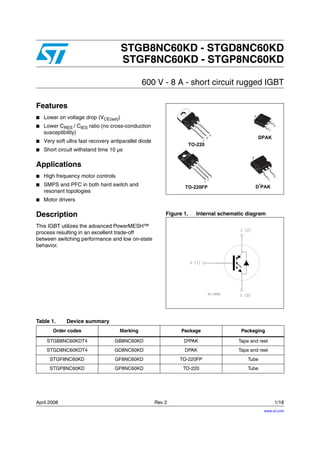
Figure 1. Internal schematic diagram
TO-220
D²
PAK
1
2
3
1
3
2
1
3
2
DPAK
1
2
3
TO-220FP
Table 1. Device summary
Order codes Marking Package Packaging
STGB8NC60KDT4 GB8NC60KD D²PAK Tape and reel
STGD8NC60KDT4 GD8NC60KD DPAK Tape and reel
STGF8NC60KD GF8NC60KD TO-220FP Tube
STGP8NC60KD GP8NC60KD TO-220 Tube
www.st.com
3. STGB8NC60KD - STGD8NC60KD - STGF8NC60KD - STGP8NC60KD Electrical ratings
3/18
1 Electrical ratings
Table 2. Absolute maximum ratings
Symbol Parameter
Value
UnitD²PAK
TO-220
DPAK TO-220FP
VCES Collector-emitter voltage (VGE = 0) 600 V
IC
(1)
1. Calculated according to the iterative formula:
Collector current (continuous) at TC = 25 °C 15 7 A
IC
(1) Collector current (continuous) at TC = 100 °C 8 4 A
ICL
(2)
2. Vclamp = 80% (VCES), VGE=15 V, RG=10 Ω, TJ=150 °C
Turn-off latching current 30 A
ICP
(3)
3. Pulse width limited by max junction temperature allowed
Pulsed collector current 30 A
VGE Gate-emitter voltage ±20 V
IF Diode RMS forward current at TC = 25 °C 7 A
IFSM
Surge not repetitive forward current
tp = 10 ms sinusoidal
20 A
VISO
Insulation withstand voltage (RMS) from all
three leads to external hea sink
( t=1 s; TC = 25 °C)
-- -- 2500 V
PTOT Total dissipation at TC = 25 °C 65 62 24 W
Tj Operating junction temperature – 55 to 150 °C
Tscw
Short circuit withstand time
(VCE = 0.5 VBR(CES) , TC = 125 °C, RG = 10 Ω,
VGE = 12 V)
10 µs
Table 3. Thermal resistance
Symbol Parameter
Value
UnitD²PAK
TO-220
DPAK TO-220FP
Rthj-case
Thermal resistance junction-case max
IGBT
1.9 2.0 5.1 °C/W
Rthj-case
Thermal resistance junction-case max
diode
4 4.5 7 °C/W
Rthj-amb Thermal resistance junction-ambient max 62.5 °C/W
I
C
T
C
( )
T
JMAX
T
C
–
R
THJ C–
V
CESAT MAX( )
T
C
I
C
,( )×
------------------------------------------------------------------------------------------------------=
4. Electrical characteristics STGB8NC60KD - STGD8NC60KD - STGF8NC60KD - STGP8NC60KD
4/18
2 Electrical characteristics
(TCASE=25°C unless otherwise specified)
Table 4. Static
Symbol Parameter Test conditions Min. Typ. Max. Unit
V(BR)CES
Collector-emitter
breakdown voltage
(VGE= 0)
IC= 1 mA 600 V
VCE(sat)
Collector-emitter saturation
voltage
VGE= 15 V, IC = 3 A
VGE= 15 V, IC = 3 A, TC = 125°C
2.2
1.8
2.75 V
V
VGE(th) Gate threshold voltage VCE= VGE, IC= 250 µA 4.5 6.5 V
ICES
Collector cut-off current
(VGE = 0)
VCE = 600 V
VCE = 600 V, TC = 125 °C
150
1
µA
mA
IGES
Gate-emitter leakage
current (VCE = 0)
VGE= ±20 V ±100 nA
gfs
(1)
1. Pulse duration = 300 us, duty cycle 1.5 %
Forward transconductance VCE = 15 V, IC= 3 A 1.9 S
Table 5. Dynamic
Symbol Parameter Test conditions Min. Typ. Max. Unit
Cies
Coes
Cres
Input capacitance
Output capacitance
Reverse transfer
capacitance
VCE = 25 V, f = 1 MHz,
VGE = 0
380
46
8.5
pF
pF
pF
Qg
Qge
Qgc
Total gate charge
Gate-emitter charge
Gate-collector charge
VCE = 390 V, IC = 3 A,
VGE = 15 V,
(see Figure 20)
19
5
9
nC
nC
nC
Table 6. Switching on/off (inductive load)
Symbol Parameter Test conditions Min. Typ. Max. Unit
td(on)
tr
(di/dt)on
Turn-on delay time
Current rise time
Turn-on current slope
VCC = 390 V, IC = 3 A
RG= 10 Ω, VGE= 15 V
(see Figure 21)
17
6
655
ns
ns
A/µs
td(on)
tr
(di/dt)on
Turn-on delay time
Current rise time
Turn-on current slope
VCC = 390 V, IC =3 A
RG= 10 Ω, VGE= 15 V,
TC = 125 °C
(see Figure 21)
16.5
6.5
575
ns
ns
A/µs
5. STGB8NC60KD - STGD8NC60KD - STGF8NC60KD - STGP8NC60KD Electrical characteristics
5/18
Symbol Parameter Test conditions Min. Typ. Max. Unit
tr(Voff)
td(off)
tf
Off voltage rise time
Turn-off delay time
Current fall time
Vcc = 390 V, IC = 3 A,
RGE = 10 Ω, VGE =15 V
(see Figure 21)
33
72
82
ns
ns
ns
tr(Voff)
td(off)
tf
Off voltage rise time
Turn-off delay time
Current fall time
Vcc = 390 V, IC = 3 A,
RGE=10 Ω, VGE =15 V,
TC = 125 °C
(see Figure 21)
60
106
136
ns
ns
ns
Table 7. Switching energy (inductive load)
Symbol Parameter Test conditions Min. Typ. Max. Unit
Eon
(1)
Eoff
(2)
Ets
1. Eon is the turn-on losses when a typical diode is used in the test circuit in figure 2. If the IGBT is offered in
a package with a co-pak diode, the co-pack diode is used as external diode. IGBTs & Diode are at the
same temperature (25°C and 125°C)
2. Turn-off losses include also the tail of the collector current
Turn-on switching losses
Turn-off switching losses
Total switching losses
VCC = 390 V, IC = 3 A
RG= 10 Ω, VGE=15 V
(see Figure 21)
55
85
140
µJ
µJ
µJ
Eon
(1)
Eoff
(2)
Ets
Turn-on switching losses
Turn-off switching losses
Total switching losses
VCC = 390 V, IC = 3 A
RG= 10 Ω, VGE= 15 V,
TC = 125 °C
(see Figure 21)
87
162
249
µJ
µJ
µJ
Table 8. Collector-emitter diode
Symbol Parameter Test conditions Min. Typ. Max. Unit
VF Forward on-voltage
IF = 3 A
IF = 3 A, TC = 125 °C
1.6
1.3
2.1 V
V
trr
Qrr
Irrm
Reverse recovery time
Reverse recovery charge
Reverse recovery current
IF = 3 A, VR = 30 V,
di/dt = 100 A/µs
(see Figure 22)
23.5
16.5
1.4
ns
nC
A
trr
Qrr
Irrm
Reverse recovery time
Reverse recovery charge
Reverse recovery current
IF = 3 A,VR = 30 V,
TC =125 °C, di/dt = 100 A/µs
(see Figure 22)
39
39
2
ns
nC
A
Table 6. Switching on/off (inductive load) (continued)
6. Electrical characteristics STGB8NC60KD - STGD8NC60KD - STGF8NC60KD - STGP8NC60KD
6/18
2.1 Electrical characteristics (curves)
Figure 2. Output characteristics Figure 3. Transfer characteristics
Figure 4. Transconductance Figure 5. Collector-emitter on voltage vs
temperature
Figure 6. Gate charge vs gate-source voltage Figure 7. Capacitance variations
7. STGB8NC60KD - STGD8NC60KD - STGF8NC60KD - STGP8NC60KD Electrical characteristics
7/18
Figure 8. Normalized gate threshold voltage
vs temperature
Figure 9. Collector-emitter on voltage vs
collector current
Figure 10. Normalized breakdown voltage vs
temperature
Figure 11. Switching losses vs temperature
Figure 12. Switching losses vs gate resistance Figure 13. Switching losses vs collector
current
8. Electrical characteristics STGB8NC60KD - STGD8NC60KD - STGF8NC60KD - STGP8NC60KD
8/18
Figure 14. Thermal impedance for TO-220/
D²PAK
Figure 15. Turn-off SOA
Figure 16. Forward voltage drop versus
forward current
Figure 17. Thermal impedance for DPAK
Figure 18. Thermal impedance for TO-220FP
9. STGB8NC60KD - STGD8NC60KD - STGF8NC60KD - STGP8NC60KD Test circuit
9/18
3 Test circuit
Figure 19. Test circuit for inductive load
switching
Figure 20. Gate charge test circuit
Figure 21. Switching waveform Figure 22. Diode recovery time waveform
10. Package mechanical data STGB8NC60KD - STGD8NC60KD - STGF8NC60KD - STGP8NC60KD
10/18
4 Package mechanical data
In order to meet environmental requirements, ST offers these devices in ECOPACK®
packages. These packages have a lead-free second level interconnect. The category of
second level interconnect is marked on the package and on the inner box label, in compliance
with JEDEC Standard JESD97. The maximum ratings related to soldering conditions are also
marked on the inner box label. ECOPACK is an ST trademark.
ECOPACK specifications are available at: www.st.com
11. STGB8NC60KD - STGD8NC60KD - STGF8NC60KD - STGP8NC60KD Package mechanical data
11/18
TO-220 mechanical data
Dim
mm inch
Min Typ Max Min Typ Max
A 4.40 4.60 0.173 0.181
b 0.61 0.88 0.024 0.034
b1 1.14 1.70 0.044 0.066
c 0.48 0.70 0.019 0.027
D 15.25 15.75 0.6 0.62
D1 1.27 0.050
E 10 10.40 0.393 0.409
e 2.40 2.70 0.094 0.106
e1 4.95 5.15 0.194 0.202
F 1.23 1.32 0.048 0.051
H1 6.20 6.60 0.244 0.256
J1 2.40 2.72 0.094 0.107
L 13 14 0.511 0.551
L1 3.50 3.93 0.137 0.154
L20 16.40 0.645
L30 28.90 1.137
∅P 3.75 3.85 0.147 0.151
Q 2.65 2.95 0.104 0.116
12. Package mechanical data STGB8NC60KD - STGD8NC60KD - STGF8NC60KD - STGP8NC60KD
12/18
DIM.
mm.
min. typ max.
A 2.20 2.40
A1 0.90 1.10
A2 0.03 0.23
b 0.64 0.90
b4 5.20 5.40
c 0.45 0.60
c2 0.48 0.60
D 6.00 6.20
D1 5.10
E 6.40 6.60
E1 4.70
e 2.28
e1 4.40 4.60
H 9.35 10.10
L 1
L1 2.80
L2 0.80
L4 0.60 1
R 0.20
V2 0 o 8 o
TO-252 (DPAK) mechanical data
0068772_G
13. STGB8NC60KD - STGD8NC60KD - STGF8NC60KD - STGP8NC60KD Package mechanical data
13/18
D²PAK (TO-263) mechanical data
Dim
mm inch
Min Typ Max Min Typ Max
A 4.40 4.60 0.173 0.181
A1 0.03 0.23 0.001 0.009
b 0.70 0.93 0.027 0.037
b2 1.14 1.70 0.045 0.067
c 0.45 0.60 0.017 0.024
c2 1.23 1.36 0.048 0.053
D 8.95 9.35 0.352 0.368
D1 7.50 0.295
E 10 10.40 0.394 0.409
E1 8.50 0.334
e 2.54 0.1
e1 4.88 5.28 0.192 0.208
H 15 15.85 0.590 0.624
J1 2.49 2.69 0.099 0.106
L 2.29 2.79 0.090 0.110
L1 1.27 1.40 0.05 0.055
L2 1.30 1.75 0.051 0.069
R 0.4 0.016
V2 0° 8° 0° 8°
0079457_M
14. Package mechanical data STGB8NC60KD - STGD8NC60KD - STGF8NC60KD - STGP8NC60KD
14/18
Dim.
mm. inch
Min. Typ Max. Min. Typ. Max.
A 4.40 4.60 0.173 0.181
B 2.5 2.7 0.098 0.106
D 2.5 2.75 0.098 0.108
E 0.45 0.70 0.017 0.027
F 0.75 1.00 0.030 0.039
F1 1.15 1.50 0.045 0.067
F2 1.15 1.50 0.045 0.067
G 4.95 5.20 0.195 0.204
G1 2.40 2.70 0.094 0.106
H 10 10.40 0.393 0.409
L2 16 0.630
L3 28.6 30.6 1.126 1.204
L4 9.80 10.60 0.385 0.417
L5 2.9 3.6 0.114 0.141
L6 15.90 16.40 0.626 0.645
L7 9 9.30 0.354 0.366
Dia 3 3.2 0.118 0.126
TO-220FP mechanical data
L2
A
B
D
E
H
G
L6
F
L3
G1
1 2 3
F2
F1
L7
L4
L5
7012510-I
Dia
15. STGB8NC60KD - STGD8NC60KD - STGF8NC60KD - STGP8NC60KD Packaging mechanical data
15/18
5 Packaging mechanical data
TAPE AND REEL SHIPMENT
D2
PAK FOOTPRINT
* on sales type
DIM.
mm inch
MIN. MAX. MIN. MAX.
A 330 12.992
B 1.5 0.059
C 12.8 13.2 0.504 0.520
D 20.2 0795
G 24.4 26.4 0.960 1.039
N 100 3.937
T 30.4 1.197
BASE QTY BULK QTY
1000 1000
REEL MECHANICAL DATA
DIM.
mm inch
MIN. MAX. MIN. MAX.
A0 10.5 10.7 0.413 0.421
B0 15.7 15.9 0.618 0.626
D 1.5 1.6 0.059 0.063
D1 1.59 1.61 0.062 0.063
E 1.65 1.85 0.065 0.073
F 11.4 11.6 0.449 0.456
K0 4.8 5.0 0.189 0.197
P0 3.9 4.1 0.153 0.161
P1 11.9 12.1 0.468 0.476
P2 1.9 2.1 0.075 0.082
R 50 1.574
T 0.25 0.35 0.0098 0.0137
W 23.7 24.3 0.933 0.956
TAPE MECHANICAL DATA
16. Packaging mechanical data STGB8NC60KD - STGD8NC60KD - STGF8NC60KD - STGP8NC60KD
16/18
TAPE AND REEL SHIPMENT
DPAK FOOTPRINT
DIM.
mm inch
MIN. MAX. MIN. MAX.
A 330 12.992
B 1.5 0.059
C 12.8 13.2 0.504 0.520
D 20.2 0.795
G 16.4 18.4 0.645 0.724
N 50 1.968
T 22.4 0.881
BASE QTY BULK QTY
2500 2500
REEL MECHANICAL DATA
DIM.
mm inch
MIN. MAX. MIN. MAX.
A0 6.8 7 0.267 0.275
B0 10.4 10.6 0.409 0.417
B1 12.1 0.476
D 1.5 1.6 0.059 0.063
D1 1.5 0.059
E 1.65 1.85 0.065 0.073
F 7.4 7.6 0.291 0.299
K0 2.55 2.75 0.100 0.108
P0 3.9 4.1 0.153 0.161
P1 7.9 8.1 0.311 0.319
P2 1.9 2.1 0.075 0.082
R 40 1.574
W 15.7 16.3 0.618 0.641
TAPE MECHANICAL DATA
All dimensions are in millimeters
17. STGB8NC60KD - STGD8NC60KD - STGF8NC60KD - STGP8NC60KD Revision history
17/18
6 Revision history
Table 9. Document revision history
Date Revision Changes
02-Oct-2007 1 First release
01-Apr-2008 2 Updated Figure 14 and Figure 17