SlideShare ist ein Scribd-Unternehmen logo
1 von 11
Faculty of Electrical and Electronic Engineering   Page         1/11
                 Department of Computer Engineering                 Session    2011/2012
                Experiment’s Title: FPGA implementation of          Semester      II
                VHDL code
AIM: To examine the decoder design using VHDL


1.0    OBJECTIVES

       (i)    To design decoder using VHDL design entry.
       (ii)   To configure and implement the design onto FPGA board.


2.0    THEORY

A VHDL code can be implemented using Field Programmable Gate Array (FPGA) board.
Figure 1 shows the general flow for programming HDL and figure 2 presents the process for
downloading a design to the target device. For this lab experiment, we will use
CPLD/FPGA trainer.


  Figure 1: General design flow diagram for programming HDL code and downloading to
                                    board/hardware.


3.0    LABORATORY REQUIREMENT:

       Personal Computer with Altera Quartus II software
       CPLD/FPGA trainer unit
Faculty of Electrical and Electronic Engineering   Page             2/11
                  Department of Computer Engineering                 Session       2011/2012
                  Experiment’s Title: FPGA implementation of         Semester          II
                  VHDL code

4.0    PROCEDURE


Starting a New Project

1.    To start working on a new design, first you have to define a new designed project.

2.    Select File | New Project Wizard to start a new project. Press Next. Set the working
      directory to be C:No.MatrikLAB2dec2to4. The project must have a name, which
      may optionally be the same as the name of the directory.

3.    Name your project as dec2to4 and press Next which leads to the window in Figure 2.
      In this window the designer can specify which existing files (if any) should be included
      in the project. We have no existing files, so click Next.


                         C:No.MatrikLAB2dec2to4


                         dec2to4


                         dec2to4


                    Figure 2: Specifying the project directory and name
Faculty of Electrical and Electronic Engineering   Page           3/11
                 Department of Computer Engineering                 Session     2011/2012
                 Experiment’s Title: FPGA implementation of         Semester        II
                 VHDL code


                     Figure 3: A window for inclusion of design files


                           Figure 4 Inclusion of other EDA tools

4.   Now, the window in Figure 4 appears, which allows the designer to specify third party
     CAD tools (i.e. those that are not a part of the Quartus II software) that should be
     used.

5.   Press Next to go to the Device Family window. Here you can specify the type of
     device in which the designed circuit will be implemented. Choose the device family
     called Cyclone.

6.   Then click Finish.
Faculty of Electrical and Electronic Engineering    Page            4/11
                  Department of Computer Engineering                  Session     2011/2012
                  Experiment’s Title: FPGA implementation of          Semester         II
                  VHDL code


Part A(1): Design 2 to 4 decoder Using VHDL
In this section, you will use Quartus II to implement logic functions by writing VHDL code.
Decoder is used to decode encoded information. In general, an x to y decoder has x select bits
and y=2x outputs.


Circuit specification
1. The 2 bit select word is denoted by w1w0 and the output lines are y0y1y2y3. Thus, this
   is called 2 to 4 decoder.

2. The truth table of 2 to 4 decoder is shown in Table 1. Each select bit w1w0 is
   equivalent of decimal number n and activates the output line by yn by setting it to logic
   „1‟ level while the remaining lines are held at logic „0‟ values.


                           Table 1 : Truth table for 2 to 4 decoder


             Figure 5: 2 to 4 decoder (a) block diagram and (b)internal circuit
Faculty of Electrical and Electronic Engineering    Page              5/11
                  Department of Computer Engineering                  Session        2011/2012
                  Experiment’s Title: FPGA implementation of          Semester           II
                  VHDL code


Design Entry
1.   Create a new project for the VHDL design in the directory C:LAB2 dec2to4. Name
     the new project as dec2to4.

2.   Select File | New, choose VHDL File, and click OK. This opens the Text Editor
     window. The first step is to specify a name for the file that will be created. Select File |
     Save As to open the Save As pop-up window. In the box labeled File name type
     dec2to4. (Make sure that the extension is VHDL File).

3.   Enter the code shown in Figure 6 into the Text Editor window. (Make sure that entity
     name must be same as file name, in this case, dec2to4).

       library IEEE;
       use IEEE.std_logic_1164.all;

       ENTITY dec2to4 IS
            PORT (w     : IN STD_LOGIC_VECTOR(1 DOWNTO 0);
                   En : IN STD_LOGIC;
                   y    : OUT STD_LOGIC_VECTOR(0 TO 3);
                    LED_COM : OUT STD_LOGIC);
       END dec2to4;

       ARCHITECTURE Behavior OF dec2to4 IS
            SIGNAL Enw : STD_LOGIC_VECTOR(2 DOWNTO 0);

       BEGIN
               Enw <= En & w;
               WITH Enw SELECT
                    y <= "1000" WHEN "100",
                          "0100" WHEN "101",
                          "0010" WHEN "110",
                          "0001" WHEN "111",
                          "0000" WHEN OTHERS;
                                LED_COM <= ‘1’;
       END Behavior;


                          Figure 6: VDHL code for 2 to 4 decoder

4.   Save the file, by using File | Save or shortcut Ctrl-s.

5.   Now synthesize your code by select Processing | Start | Start Analysis and
     Synthesis.

6.   Run the Compiler by selecting Processing | Start Compilation. Successful (or
     unsuccessful) compilation is indicated in a pop-up box. View the report by selecting
     Processing | Compilation Report. If the compilation is unsuccessful, expand the
     Analysis & Synthesis part of the report and then select Messages to have the
Faculty of Electrical and Electronic Engineering   Page            6/11
                   Department of Computer Engineering                 Session      2011/2012
                  Experiment’s Title: FPGA implementation of        Semester        II
                  VHDL code
     Messages displayed. Double-click on the first error message or select Errors.
     Quartus II software responds By opening the VHDL file and highlighting the statement
     which is affected by the error. Correct the error and recompile the design.

7.   Perform the functional and timing simulation, verify and discuss your result in the
     report. Before the circuit can be simulated, it is necessary to create the desired
     waveforms, called test vectors, to represent the input signals.

     a. Open the Waveform Editor window by selecting File | New. Click on the Other
        Files tab. Choose Vector Waveform File and click OK.


     b. The Waveform Editor window will appear. Save the file under the name
        dec2to4.vwf.

     c. Set the desired simulation to run from 0 to 160 ns by selecting Edit | End Time
        and entering 160 ns in the dialog box that pops up. Select View | Fit in Window
        to display the entire simulation range of 0 to 160 ns in the window.

     d. Next, you must include the input and output nodes of the circuit to be simulated.
        This is done by using the Node Finder utility. Click Edit | Insert Node or Bus to
        open the Insert Node or Bus window.

     e. Click Node Finder… button to list out all nodes in the circuit. Since we are
        interested in input and output pins, set the filter to Pins: all. Click the List button
        to find the input and output nodes.

     f.   Set the variation of inputs.

     g. A circuit can be simulated in two ways. The simplest way is to assume that logic
        elements and interconnection wires are perfect, thus causing no delay in
        propagation of signals through the circuit. This is called functional simulation. To
        perform the functional simulation, select Assignments | Setting to open the
        Settings window. On the left side of this window, click on Simulator and choose
        Functional as the simulation mode. Click OK and save the waveform as
        dec2to4.vwf.

     h. To complete the set up of the simulator select the command Processing |
        Generate Functional Simulation Netlist.

     i.   Run the simulation process by select Processing | Start Simulation. After the
          simulation process is completed, press open to view the simulation result.

     j.   Repeat step g and i for timing simulation.


(Q1) Sketch functional simulation waveform for VHDL code in figure 6. (2 marks)
(Q2) Sketch timing simulation waveform for VHDL code in figure 6. (2 marks)
(Q3) Analyze the results for both functional and timing simulations. (10 marks)
Faculty of Electrical and Electronic Engineering   Page            7/11
                 Department of Computer Engineering                 Session      2011/2012
                 Experiment’s Title: FPGA implementation of         Semester         II
                 VHDL code


Part A(2): Download 2 to 4 decoder code on CPLD/FPGA board.
Floorplan

8. Go back to the “dec2to4.vhd” file.

9. Select the FLEX10K – EPF10K10TC144-4 device by selecting Assignment | Device
   from the menu bar. Next, assign pin numbers to all of the input and output nodes using
   Table 2 as a reference.

                          Table 2 – Pin assignments for dec2to4
            Node Type            Node          Pin Number              Device
                                   En                47                 SW1
             INPUTS               w0                 48                 SW2
                                  w1                 49                 SW3
                                   y0                20                  L12
                                   y1                19                  L11
             OUTPUT                y2                18                  L10
                                   y3                17                   L9
                              LED_COM               141               LED_COM

10. To assign a pin, select Assignment | Pins. The pin assignment window will
    appear. To assign pin number 51 to node “SW1”, Select the pin number 51 in
    “Location” text box and type “SW1” in the “pin name” text box. Repeat the pin
    assignment process for the other nodes.

11. Then, compile the design.


Download and Test

12.    Start the programmer by selecting Tools | Programmer to open the programmer
       window.

13.    Switch on the CPLD/FPGA trainer unit. Next, in the programmer window, click
       Hardware Setup button. In the hardware setup window, click the Add Hardware
       button. Select ByteBlaster II for hardware type and LPT1 for the port. Next,
       highlight the ByteBlaster II and click Select Hardware button. This will enable the
       Start button in programmer window.

14.   Alternatively, we can click Add File button to add the SRAM Object File (*.sof) (in
      this case, “dec2to4.sof”). Next, Click the start button to download the design to
      the target hardware.

15.    Test and verify the circuit by pressing the SWs push buttons and observing
       LEDs.

(Q4) Compute a truth table associated with your observation on LEDs. (8 marks)
(Q5) Write a brief discussion for your experience on the process of realizing 2-to-4
     decoder using FPGA. (15 marks)
Faculty of Electrical and Electronic Engineering   Page           8/11
                 Department of Computer Engineering                 Session     2011/2012
                Experiment’s Title: FPGA implementation of          Semester        II
                VHDL code
(Q6) Write a summary for Part A. (5 marks)

Part B(1): Design 3 to 8 Decoder using VHDL

Circuit Specification

3 to 8 decoder can be constructed with two 2 to 4 decoder and other additional gates. This
is done by define the decoder 2 to 4 as a component in the package. The component
declaration allows the entity to be used as a sub circuit in other VHDL code.

Design Entry
1.   Create a new project for the VHDL design in the directory C:LAB2dec3to8. Name
     the new project as dec3to8.

2.   Repeat the procedure in Part A 1 – 6. With the aid of Quartus II, write the VHDL code
     using structural modeling that implement the circuit in Figure 7. Save the file as a
     dec3to8.vhd.


                   Figure 7 : 3 to 8 decoder using 2 to 4 decoder circuit


(Q7) Compute VHDL code for implementing the 3-to-8 decoder in Figure 7. (10
     marks)
(Q8) Sketch timing simulation waveform for 3-to-8 decoder in Figure 7. (4 marks)
(Q9) Analyze the simulation result. (10 marks)
Faculty of Electrical and Electronic Engineering   Page            9/11
                      Department of Computer Engineering                 Session    2011/2012
                      Experiment’s Title: FPGA implementation of         Semester         II
                      VHDL code

    Part B(2): Download 3 to 8 decoder code on CPLD/FPGA board.
    Floorplan

    3. Go back to the “dec3to8.vhd” file.

    4. Select the FLEX10K – EPF10K10TC144-4 device by selecting Assignment | Device
       from the menu bar. Next, assign pin numbers to all of the input and output nodes using
       Table 3 as a reference.

                        Table 3 – Pin assignments for 3 to 8 decoder
                Node Type       Node          Pin Number             Device
                                  En                 47               SW1
                                  w0                 48               SW2
                 INPUTS
                                  w1                 49               SW3
                                  w2                 51               SW4
                                  y0                 20               L12
                                  y1                 19               L11
                                  y2                 18               L10
                                  y3                 17                L9
                OUTPUTS           y4                 14                L8
                                  y5                 13                L7
                                  y6                 12                L6
                                  y7                 11                L5
                              LED_COM               141           LED_COM


.   5.    To assign a pin, select Assignment | Pins. The pin assignment window will
         appear. To assign pin number 47 to node “SW4”, Select the pin number 47 in
         “Location” text box and type “SW4” in the “pin name” text box. Repeat the pin
         assignment process for the other nodes.


    6.    Then, compile the design.

    7.    Download the program by start the programmer by selecting Tools | Programmer to
          open the programmer window.

    8.   Test and verify the circuit by pressing the SWs push buttons and observing LEDs.


    (Q10)Compute a truth table associated with your observation on LEDs. (8 marks)
    (Q11) Write a brief discussion on your experience for developing 3-to-8 decoder
         using FPGA. (15 marks)
    (Q12) Write a summary for the task done in Part B. (5 marks)
Faculty of Electrical and Electronic Engineering   Page         10/11
                 Department of Computer Engineering                 Session    2011/2012
                 Experiment’s Title: FPGA implementation of         Semester      II
                 VHDL code


QUESTIONS
1. Briefly explain the VHDL code in Fig.1. (4 marks)
          Enw <= En & w;
                 WITH Enw SELECT
                        y <= "1000" WHEN "100",
                               "0100" WHEN "101",
                               "0010" WHEN "110",
                               "0001" WHEN "111",
                               "0000" WHEN OTHERS;

                         Fig. 1


2. Rewrite the VHDL code in Fig. 1 using conditional assignment statement. (6 marks)

3. State four (4) advantages of using VHDL design entry compared with schematic design
   entry. (4 marks)

4. Describe two approaches for declaring a VHDL code as sub-circuit in another VHDL
   code. (6 marks)


INSTRUCTION
This report must be completed and submit to the laboratory instructor ONE day after the
laboratory session.
Your report must include all the questions in Question Section.
The report must be compiled with your handwriting.
Faculty of Electrical and Electronic Engineering   Page         11/11
Department of Computer Engineering                 Session    2011/2012
Experiment’s Title: FPGA implementation of         Semester      II
VHDL code

Weitere ähnliche Inhalte

Was ist angesagt?

Was ist angesagt? (20)

Introduction to-vhdl
Introduction to-vhdlIntroduction to-vhdl
Introduction to-vhdl
 
Verilog HDL Training Course
Verilog HDL Training CourseVerilog HDL Training Course
Verilog HDL Training Course
 
Verilog Tutorial - Verilog HDL Tutorial with Examples
Verilog Tutorial - Verilog HDL Tutorial with ExamplesVerilog Tutorial - Verilog HDL Tutorial with Examples
Verilog Tutorial - Verilog HDL Tutorial with Examples
 
Digital design with Systemc
Digital design with SystemcDigital design with Systemc
Digital design with Systemc
 
EC6612 VLSI Design Lab Manual
EC6612 VLSI Design Lab ManualEC6612 VLSI Design Lab Manual
EC6612 VLSI Design Lab Manual
 
verilog
verilogverilog
verilog
 
How to design Programs using VHDL
How to design Programs using VHDLHow to design Programs using VHDL
How to design Programs using VHDL
 
Verilog HDL - 3
Verilog HDL - 3Verilog HDL - 3
Verilog HDL - 3
 
Verilog tutorial
Verilog tutorialVerilog tutorial
Verilog tutorial
 
Vhdl programming
Vhdl programmingVhdl programming
Vhdl programming
 
Lecture1
Lecture1Lecture1
Lecture1
 
Verilog HDL- 2
Verilog HDL- 2Verilog HDL- 2
Verilog HDL- 2
 
Vlsi lab manual exp:1
Vlsi lab manual exp:1Vlsi lab manual exp:1
Vlsi lab manual exp:1
 
Vhdl
VhdlVhdl
Vhdl
 
VHDL CODES
VHDL CODES VHDL CODES
VHDL CODES
 
System Verilog Tutorial - VHDL
System Verilog Tutorial - VHDLSystem Verilog Tutorial - VHDL
System Verilog Tutorial - VHDL
 
Vhdl introduction
Vhdl introductionVhdl introduction
Vhdl introduction
 
VTU ECE 7th sem VLSI lab manual
VTU ECE 7th sem VLSI lab manualVTU ECE 7th sem VLSI lab manual
VTU ECE 7th sem VLSI lab manual
 
VHDL
VHDLVHDL
VHDL
 
Chapter 5 introduction to VHDL
Chapter 5 introduction to VHDLChapter 5 introduction to VHDL
Chapter 5 introduction to VHDL
 

Andere mochten auch

Connected Cars - Use Cases for Indian Scenario
Connected Cars - Use Cases for Indian ScenarioConnected Cars - Use Cases for Indian Scenario
Connected Cars - Use Cases for Indian ScenarioHCL Technologies
 
Internet Of Things in Automobile Industry
Internet Of Things in Automobile IndustryInternet Of Things in Automobile Industry
Internet Of Things in Automobile IndustryIEI GSC
 
The Internet of Cars - Towards the Future of the Connected Car
The Internet of Cars - Towards the Future of the Connected CarThe Internet of Cars - Towards the Future of the Connected Car
The Internet of Cars - Towards the Future of the Connected CarJorgen Thelin
 
The Connected Car: Driving Towards the Future
The Connected Car: Driving Towards the FutureThe Connected Car: Driving Towards the Future
The Connected Car: Driving Towards the FutureNudge Software Inc.
 

Andere mochten auch (7)

Connected Cars - Use Cases for Indian Scenario
Connected Cars - Use Cases for Indian ScenarioConnected Cars - Use Cases for Indian Scenario
Connected Cars - Use Cases for Indian Scenario
 
Internet Of Things in Automobile Industry
Internet Of Things in Automobile IndustryInternet Of Things in Automobile Industry
Internet Of Things in Automobile Industry
 
Connected Car Technology
Connected Car TechnologyConnected Car Technology
Connected Car Technology
 
The Internet of Cars - Towards the Future of the Connected Car
The Internet of Cars - Towards the Future of the Connected CarThe Internet of Cars - Towards the Future of the Connected Car
The Internet of Cars - Towards the Future of the Connected Car
 
The Connected Car: Driving Towards the Future
The Connected Car: Driving Towards the FutureThe Connected Car: Driving Towards the Future
The Connected Car: Driving Towards the Future
 
Stp chapter 7
Stp  chapter 7Stp  chapter 7
Stp chapter 7
 
Customer driven marketing strategy
Customer driven marketing strategyCustomer driven marketing strategy
Customer driven marketing strategy
 

Ähnlich wie FPGA VHDL Decoder

Lab mke1503 mee10203 01
Lab mke1503 mee10203 01Lab mke1503 mee10203 01
Lab mke1503 mee10203 01wanrizegillah
 
verilog basics.ppt
verilog basics.pptverilog basics.ppt
verilog basics.ppt8885684828
 
generate IP CORES
generate IP CORESgenerate IP CORES
generate IP CORESguest296013
 
Xilinx ISE introduction Tutorial #1
Xilinx ISE introduction Tutorial #1Xilinx ISE introduction Tutorial #1
Xilinx ISE introduction Tutorial #1guest1e88645e
 
Micro c lab2(led patterns)
Micro c lab2(led patterns)Micro c lab2(led patterns)
Micro c lab2(led patterns)Mashood
 
Verilog overview
Verilog overviewVerilog overview
Verilog overviewposdege
 
Z turn Board Tutorial Book
Z turn Board Tutorial BookZ turn Board Tutorial Book
Z turn Board Tutorial BookLinda Zhang
 
15LLP108_Demo4_LedBlinking.pdf1. Introduction In D.docx
15LLP108_Demo4_LedBlinking.pdf1. Introduction In D.docx15LLP108_Demo4_LedBlinking.pdf1. Introduction In D.docx
15LLP108_Demo4_LedBlinking.pdf1. Introduction In D.docxfelicidaddinwoodie
 
Developing new zynq based instruments
Developing new zynq based instrumentsDeveloping new zynq based instruments
Developing new zynq based instrumentsGraham NAYLOR
 
The Principle Of Ultrasound Imaging System
The Principle Of Ultrasound Imaging SystemThe Principle Of Ultrasound Imaging System
The Principle Of Ultrasound Imaging SystemMelissa Luster
 
15EE51 - Microcontrollers Laboratory
15EE51 - Microcontrollers Laboratory15EE51 - Microcontrollers Laboratory
15EE51 - Microcontrollers LaboratoryJabez Winston
 
Filter designandanalysisusingmicrowaveoffice
Filter designandanalysisusingmicrowaveofficeFilter designandanalysisusingmicrowaveoffice
Filter designandanalysisusingmicrowaveofficeEmad S. Ahmed
 
Experiment_1.pdf
Experiment_1.pdfExperiment_1.pdf
Experiment_1.pdfmusa572502
 

Ähnlich wie FPGA VHDL Decoder (20)

Lab mke1503 mee10203 01
Lab mke1503 mee10203 01Lab mke1503 mee10203 01
Lab mke1503 mee10203 01
 
verilog basics.ppt
verilog basics.pptverilog basics.ppt
verilog basics.ppt
 
generate IP CORES
generate IP CORESgenerate IP CORES
generate IP CORES
 
Xilinx ISE introduction Tutorial #1
Xilinx ISE introduction Tutorial #1Xilinx ISE introduction Tutorial #1
Xilinx ISE introduction Tutorial #1
 
Vhdl design flow
Vhdl design flowVhdl design flow
Vhdl design flow
 
Micro c lab2(led patterns)
Micro c lab2(led patterns)Micro c lab2(led patterns)
Micro c lab2(led patterns)
 
Verilog overview
Verilog overviewVerilog overview
Verilog overview
 
Xilinx verilog tutorial
Xilinx verilog tutorialXilinx verilog tutorial
Xilinx verilog tutorial
 
Z turn Board Tutorial Book
Z turn Board Tutorial BookZ turn Board Tutorial Book
Z turn Board Tutorial Book
 
15LLP108_Demo4_LedBlinking.pdf1. Introduction In D.docx
15LLP108_Demo4_LedBlinking.pdf1. Introduction In D.docx15LLP108_Demo4_LedBlinking.pdf1. Introduction In D.docx
15LLP108_Demo4_LedBlinking.pdf1. Introduction In D.docx
 
STM -32
STM -32STM -32
STM -32
 
learning STM -32
learning STM -32 learning STM -32
learning STM -32
 
Verilog tutorial
Verilog tutorialVerilog tutorial
Verilog tutorial
 
Developing new zynq based instruments
Developing new zynq based instrumentsDeveloping new zynq based instruments
Developing new zynq based instruments
 
The Principle Of Ultrasound Imaging System
The Principle Of Ultrasound Imaging SystemThe Principle Of Ultrasound Imaging System
The Principle Of Ultrasound Imaging System
 
15EE51 - Microcontrollers Laboratory
15EE51 - Microcontrollers Laboratory15EE51 - Microcontrollers Laboratory
15EE51 - Microcontrollers Laboratory
 
Altera up1
Altera up1Altera up1
Altera up1
 
Ecad final
Ecad finalEcad final
Ecad final
 
Filter designandanalysisusingmicrowaveoffice
Filter designandanalysisusingmicrowaveofficeFilter designandanalysisusingmicrowaveoffice
Filter designandanalysisusingmicrowaveoffice
 
Experiment_1.pdf
Experiment_1.pdfExperiment_1.pdf
Experiment_1.pdf
 

Kürzlich hochgeladen

Virtual-Orientation-on-the-Administration-of-NATG12-NATG6-and-ELLNA.pdf
Virtual-Orientation-on-the-Administration-of-NATG12-NATG6-and-ELLNA.pdfVirtual-Orientation-on-the-Administration-of-NATG12-NATG6-and-ELLNA.pdf
Virtual-Orientation-on-the-Administration-of-NATG12-NATG6-and-ELLNA.pdfErwinPantujan2
 
Music 9 - 4th quarter - Vocal Music of the Romantic Period.pptx
Music 9 - 4th quarter - Vocal Music of the Romantic Period.pptxMusic 9 - 4th quarter - Vocal Music of the Romantic Period.pptx
Music 9 - 4th quarter - Vocal Music of the Romantic Period.pptxleah joy valeriano
 
Field Attribute Index Feature in Odoo 17
Field Attribute Index Feature in Odoo 17Field Attribute Index Feature in Odoo 17
Field Attribute Index Feature in Odoo 17Celine George
 
GRADE 4 - SUMMATIVE TEST QUARTER 4 ALL SUBJECTS
GRADE 4 - SUMMATIVE TEST QUARTER 4 ALL SUBJECTSGRADE 4 - SUMMATIVE TEST QUARTER 4 ALL SUBJECTS
GRADE 4 - SUMMATIVE TEST QUARTER 4 ALL SUBJECTSJoshuaGantuangco2
 
Inclusivity Essentials_ Creating Accessible Websites for Nonprofits .pdf
Inclusivity Essentials_ Creating Accessible Websites for Nonprofits .pdfInclusivity Essentials_ Creating Accessible Websites for Nonprofits .pdf
Inclusivity Essentials_ Creating Accessible Websites for Nonprofits .pdfTechSoup
 
Daily Lesson Plan in Mathematics Quarter 4
Daily Lesson Plan in Mathematics Quarter 4Daily Lesson Plan in Mathematics Quarter 4
Daily Lesson Plan in Mathematics Quarter 4JOYLYNSAMANIEGO
 
ANG SEKTOR NG agrikultura.pptx QUARTER 4
ANG SEKTOR NG agrikultura.pptx QUARTER 4ANG SEKTOR NG agrikultura.pptx QUARTER 4
ANG SEKTOR NG agrikultura.pptx QUARTER 4MiaBumagat1
 
ICS2208 Lecture6 Notes for SL spaces.pdf
ICS2208 Lecture6 Notes for SL spaces.pdfICS2208 Lecture6 Notes for SL spaces.pdf
ICS2208 Lecture6 Notes for SL spaces.pdfVanessa Camilleri
 
Influencing policy (training slides from Fast Track Impact)
Influencing policy (training slides from Fast Track Impact)Influencing policy (training slides from Fast Track Impact)
Influencing policy (training slides from Fast Track Impact)Mark Reed
 
Student Profile Sample - We help schools to connect the data they have, with ...
Student Profile Sample - We help schools to connect the data they have, with ...Student Profile Sample - We help schools to connect the data they have, with ...
Student Profile Sample - We help schools to connect the data they have, with ...Seán Kennedy
 
Full Stack Web Development Course for Beginners
Full Stack Web Development Course  for BeginnersFull Stack Web Development Course  for Beginners
Full Stack Web Development Course for BeginnersSabitha Banu
 
THEORIES OF ORGANIZATION-PUBLIC ADMINISTRATION
THEORIES OF ORGANIZATION-PUBLIC ADMINISTRATIONTHEORIES OF ORGANIZATION-PUBLIC ADMINISTRATION
THEORIES OF ORGANIZATION-PUBLIC ADMINISTRATIONHumphrey A Beña
 
4.16.24 21st Century Movements for Black Lives.pptx
4.16.24 21st Century Movements for Black Lives.pptx4.16.24 21st Century Movements for Black Lives.pptx
4.16.24 21st Century Movements for Black Lives.pptxmary850239
 
What is Model Inheritance in Odoo 17 ERP
What is Model Inheritance in Odoo 17 ERPWhat is Model Inheritance in Odoo 17 ERP
What is Model Inheritance in Odoo 17 ERPCeline George
 
Global Lehigh Strategic Initiatives (without descriptions)
Global Lehigh Strategic Initiatives (without descriptions)Global Lehigh Strategic Initiatives (without descriptions)
Global Lehigh Strategic Initiatives (without descriptions)cama23
 
Barangay Council for the Protection of Children (BCPC) Orientation.pptx
Barangay Council for the Protection of Children (BCPC) Orientation.pptxBarangay Council for the Protection of Children (BCPC) Orientation.pptx
Barangay Council for the Protection of Children (BCPC) Orientation.pptxCarlos105
 
Choosing the Right CBSE School A Comprehensive Guide for Parents
Choosing the Right CBSE School A Comprehensive Guide for ParentsChoosing the Right CBSE School A Comprehensive Guide for Parents
Choosing the Right CBSE School A Comprehensive Guide for Parentsnavabharathschool99
 
Incoming and Outgoing Shipments in 3 STEPS Using Odoo 17
Incoming and Outgoing Shipments in 3 STEPS Using Odoo 17Incoming and Outgoing Shipments in 3 STEPS Using Odoo 17
Incoming and Outgoing Shipments in 3 STEPS Using Odoo 17Celine George
 
Difference Between Search & Browse Methods in Odoo 17
Difference Between Search & Browse Methods in Odoo 17Difference Between Search & Browse Methods in Odoo 17
Difference Between Search & Browse Methods in Odoo 17Celine George
 

Kürzlich hochgeladen (20)

Virtual-Orientation-on-the-Administration-of-NATG12-NATG6-and-ELLNA.pdf
Virtual-Orientation-on-the-Administration-of-NATG12-NATG6-and-ELLNA.pdfVirtual-Orientation-on-the-Administration-of-NATG12-NATG6-and-ELLNA.pdf
Virtual-Orientation-on-the-Administration-of-NATG12-NATG6-and-ELLNA.pdf
 
Music 9 - 4th quarter - Vocal Music of the Romantic Period.pptx
Music 9 - 4th quarter - Vocal Music of the Romantic Period.pptxMusic 9 - 4th quarter - Vocal Music of the Romantic Period.pptx
Music 9 - 4th quarter - Vocal Music of the Romantic Period.pptx
 
Field Attribute Index Feature in Odoo 17
Field Attribute Index Feature in Odoo 17Field Attribute Index Feature in Odoo 17
Field Attribute Index Feature in Odoo 17
 
GRADE 4 - SUMMATIVE TEST QUARTER 4 ALL SUBJECTS
GRADE 4 - SUMMATIVE TEST QUARTER 4 ALL SUBJECTSGRADE 4 - SUMMATIVE TEST QUARTER 4 ALL SUBJECTS
GRADE 4 - SUMMATIVE TEST QUARTER 4 ALL SUBJECTS
 
Inclusivity Essentials_ Creating Accessible Websites for Nonprofits .pdf
Inclusivity Essentials_ Creating Accessible Websites for Nonprofits .pdfInclusivity Essentials_ Creating Accessible Websites for Nonprofits .pdf
Inclusivity Essentials_ Creating Accessible Websites for Nonprofits .pdf
 
Daily Lesson Plan in Mathematics Quarter 4
Daily Lesson Plan in Mathematics Quarter 4Daily Lesson Plan in Mathematics Quarter 4
Daily Lesson Plan in Mathematics Quarter 4
 
ANG SEKTOR NG agrikultura.pptx QUARTER 4
ANG SEKTOR NG agrikultura.pptx QUARTER 4ANG SEKTOR NG agrikultura.pptx QUARTER 4
ANG SEKTOR NG agrikultura.pptx QUARTER 4
 
ICS2208 Lecture6 Notes for SL spaces.pdf
ICS2208 Lecture6 Notes for SL spaces.pdfICS2208 Lecture6 Notes for SL spaces.pdf
ICS2208 Lecture6 Notes for SL spaces.pdf
 
Influencing policy (training slides from Fast Track Impact)
Influencing policy (training slides from Fast Track Impact)Influencing policy (training slides from Fast Track Impact)
Influencing policy (training slides from Fast Track Impact)
 
Student Profile Sample - We help schools to connect the data they have, with ...
Student Profile Sample - We help schools to connect the data they have, with ...Student Profile Sample - We help schools to connect the data they have, with ...
Student Profile Sample - We help schools to connect the data they have, with ...
 
Full Stack Web Development Course for Beginners
Full Stack Web Development Course  for BeginnersFull Stack Web Development Course  for Beginners
Full Stack Web Development Course for Beginners
 
THEORIES OF ORGANIZATION-PUBLIC ADMINISTRATION
THEORIES OF ORGANIZATION-PUBLIC ADMINISTRATIONTHEORIES OF ORGANIZATION-PUBLIC ADMINISTRATION
THEORIES OF ORGANIZATION-PUBLIC ADMINISTRATION
 
4.16.24 21st Century Movements for Black Lives.pptx
4.16.24 21st Century Movements for Black Lives.pptx4.16.24 21st Century Movements for Black Lives.pptx
4.16.24 21st Century Movements for Black Lives.pptx
 
YOUVE GOT EMAIL_FINALS_EL_DORADO_2024.pptx
YOUVE GOT EMAIL_FINALS_EL_DORADO_2024.pptxYOUVE GOT EMAIL_FINALS_EL_DORADO_2024.pptx
YOUVE GOT EMAIL_FINALS_EL_DORADO_2024.pptx
 
What is Model Inheritance in Odoo 17 ERP
What is Model Inheritance in Odoo 17 ERPWhat is Model Inheritance in Odoo 17 ERP
What is Model Inheritance in Odoo 17 ERP
 
Global Lehigh Strategic Initiatives (without descriptions)
Global Lehigh Strategic Initiatives (without descriptions)Global Lehigh Strategic Initiatives (without descriptions)
Global Lehigh Strategic Initiatives (without descriptions)
 
Barangay Council for the Protection of Children (BCPC) Orientation.pptx
Barangay Council for the Protection of Children (BCPC) Orientation.pptxBarangay Council for the Protection of Children (BCPC) Orientation.pptx
Barangay Council for the Protection of Children (BCPC) Orientation.pptx
 
Choosing the Right CBSE School A Comprehensive Guide for Parents
Choosing the Right CBSE School A Comprehensive Guide for ParentsChoosing the Right CBSE School A Comprehensive Guide for Parents
Choosing the Right CBSE School A Comprehensive Guide for Parents
 
Incoming and Outgoing Shipments in 3 STEPS Using Odoo 17
Incoming and Outgoing Shipments in 3 STEPS Using Odoo 17Incoming and Outgoing Shipments in 3 STEPS Using Odoo 17
Incoming and Outgoing Shipments in 3 STEPS Using Odoo 17
 
Difference Between Search & Browse Methods in Odoo 17
Difference Between Search & Browse Methods in Odoo 17Difference Between Search & Browse Methods in Odoo 17
Difference Between Search & Browse Methods in Odoo 17
 

FPGA VHDL Decoder

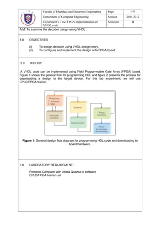
  • 1. Faculty of Electrical and Electronic Engineering Page 1/11 Department of Computer Engineering Session 2011/2012 Experiment’s Title: FPGA implementation of Semester II VHDL code AIM: To examine the decoder design using VHDL 1.0 OBJECTIVES (i) To design decoder using VHDL design entry. (ii) To configure and implement the design onto FPGA board. 2.0 THEORY A VHDL code can be implemented using Field Programmable Gate Array (FPGA) board. Figure 1 shows the general flow for programming HDL and figure 2 presents the process for downloading a design to the target device. For this lab experiment, we will use CPLD/FPGA trainer. Figure 1: General design flow diagram for programming HDL code and downloading to board/hardware. 3.0 LABORATORY REQUIREMENT: Personal Computer with Altera Quartus II software CPLD/FPGA trainer unit
  • 2. Faculty of Electrical and Electronic Engineering Page 2/11 Department of Computer Engineering Session 2011/2012 Experiment’s Title: FPGA implementation of Semester II VHDL code 4.0 PROCEDURE Starting a New Project 1. To start working on a new design, first you have to define a new designed project. 2. Select File | New Project Wizard to start a new project. Press Next. Set the working directory to be C:No.MatrikLAB2dec2to4. The project must have a name, which may optionally be the same as the name of the directory. 3. Name your project as dec2to4 and press Next which leads to the window in Figure 2. In this window the designer can specify which existing files (if any) should be included in the project. We have no existing files, so click Next. C:No.MatrikLAB2dec2to4 dec2to4 dec2to4 Figure 2: Specifying the project directory and name
  • 3. Faculty of Electrical and Electronic Engineering Page 3/11 Department of Computer Engineering Session 2011/2012 Experiment’s Title: FPGA implementation of Semester II VHDL code Figure 3: A window for inclusion of design files Figure 4 Inclusion of other EDA tools 4. Now, the window in Figure 4 appears, which allows the designer to specify third party CAD tools (i.e. those that are not a part of the Quartus II software) that should be used. 5. Press Next to go to the Device Family window. Here you can specify the type of device in which the designed circuit will be implemented. Choose the device family called Cyclone. 6. Then click Finish.
  • 4. Faculty of Electrical and Electronic Engineering Page 4/11 Department of Computer Engineering Session 2011/2012 Experiment’s Title: FPGA implementation of Semester II VHDL code Part A(1): Design 2 to 4 decoder Using VHDL In this section, you will use Quartus II to implement logic functions by writing VHDL code. Decoder is used to decode encoded information. In general, an x to y decoder has x select bits and y=2x outputs. Circuit specification 1. The 2 bit select word is denoted by w1w0 and the output lines are y0y1y2y3. Thus, this is called 2 to 4 decoder. 2. The truth table of 2 to 4 decoder is shown in Table 1. Each select bit w1w0 is equivalent of decimal number n and activates the output line by yn by setting it to logic „1‟ level while the remaining lines are held at logic „0‟ values. Table 1 : Truth table for 2 to 4 decoder Figure 5: 2 to 4 decoder (a) block diagram and (b)internal circuit
  • 5. Faculty of Electrical and Electronic Engineering Page 5/11 Department of Computer Engineering Session 2011/2012 Experiment’s Title: FPGA implementation of Semester II VHDL code Design Entry 1. Create a new project for the VHDL design in the directory C:LAB2 dec2to4. Name the new project as dec2to4. 2. Select File | New, choose VHDL File, and click OK. This opens the Text Editor window. The first step is to specify a name for the file that will be created. Select File | Save As to open the Save As pop-up window. In the box labeled File name type dec2to4. (Make sure that the extension is VHDL File). 3. Enter the code shown in Figure 6 into the Text Editor window. (Make sure that entity name must be same as file name, in this case, dec2to4). library IEEE; use IEEE.std_logic_1164.all; ENTITY dec2to4 IS PORT (w : IN STD_LOGIC_VECTOR(1 DOWNTO 0); En : IN STD_LOGIC; y : OUT STD_LOGIC_VECTOR(0 TO 3); LED_COM : OUT STD_LOGIC); END dec2to4; ARCHITECTURE Behavior OF dec2to4 IS SIGNAL Enw : STD_LOGIC_VECTOR(2 DOWNTO 0); BEGIN Enw <= En & w; WITH Enw SELECT y <= "1000" WHEN "100", "0100" WHEN "101", "0010" WHEN "110", "0001" WHEN "111", "0000" WHEN OTHERS; LED_COM <= ‘1’; END Behavior; Figure 6: VDHL code for 2 to 4 decoder 4. Save the file, by using File | Save or shortcut Ctrl-s. 5. Now synthesize your code by select Processing | Start | Start Analysis and Synthesis. 6. Run the Compiler by selecting Processing | Start Compilation. Successful (or unsuccessful) compilation is indicated in a pop-up box. View the report by selecting Processing | Compilation Report. If the compilation is unsuccessful, expand the Analysis & Synthesis part of the report and then select Messages to have the
  • 6. Faculty of Electrical and Electronic Engineering Page 6/11 Department of Computer Engineering Session 2011/2012 Experiment’s Title: FPGA implementation of Semester II VHDL code Messages displayed. Double-click on the first error message or select Errors. Quartus II software responds By opening the VHDL file and highlighting the statement which is affected by the error. Correct the error and recompile the design. 7. Perform the functional and timing simulation, verify and discuss your result in the report. Before the circuit can be simulated, it is necessary to create the desired waveforms, called test vectors, to represent the input signals. a. Open the Waveform Editor window by selecting File | New. Click on the Other Files tab. Choose Vector Waveform File and click OK. b. The Waveform Editor window will appear. Save the file under the name dec2to4.vwf. c. Set the desired simulation to run from 0 to 160 ns by selecting Edit | End Time and entering 160 ns in the dialog box that pops up. Select View | Fit in Window to display the entire simulation range of 0 to 160 ns in the window. d. Next, you must include the input and output nodes of the circuit to be simulated. This is done by using the Node Finder utility. Click Edit | Insert Node or Bus to open the Insert Node or Bus window. e. Click Node Finder… button to list out all nodes in the circuit. Since we are interested in input and output pins, set the filter to Pins: all. Click the List button to find the input and output nodes. f. Set the variation of inputs. g. A circuit can be simulated in two ways. The simplest way is to assume that logic elements and interconnection wires are perfect, thus causing no delay in propagation of signals through the circuit. This is called functional simulation. To perform the functional simulation, select Assignments | Setting to open the Settings window. On the left side of this window, click on Simulator and choose Functional as the simulation mode. Click OK and save the waveform as dec2to4.vwf. h. To complete the set up of the simulator select the command Processing | Generate Functional Simulation Netlist. i. Run the simulation process by select Processing | Start Simulation. After the simulation process is completed, press open to view the simulation result. j. Repeat step g and i for timing simulation. (Q1) Sketch functional simulation waveform for VHDL code in figure 6. (2 marks) (Q2) Sketch timing simulation waveform for VHDL code in figure 6. (2 marks) (Q3) Analyze the results for both functional and timing simulations. (10 marks)
  • 7. Faculty of Electrical and Electronic Engineering Page 7/11 Department of Computer Engineering Session 2011/2012 Experiment’s Title: FPGA implementation of Semester II VHDL code Part A(2): Download 2 to 4 decoder code on CPLD/FPGA board. Floorplan 8. Go back to the “dec2to4.vhd” file. 9. Select the FLEX10K – EPF10K10TC144-4 device by selecting Assignment | Device from the menu bar. Next, assign pin numbers to all of the input and output nodes using Table 2 as a reference. Table 2 – Pin assignments for dec2to4 Node Type Node Pin Number Device En 47 SW1 INPUTS w0 48 SW2 w1 49 SW3 y0 20 L12 y1 19 L11 OUTPUT y2 18 L10 y3 17 L9 LED_COM 141 LED_COM 10. To assign a pin, select Assignment | Pins. The pin assignment window will appear. To assign pin number 51 to node “SW1”, Select the pin number 51 in “Location” text box and type “SW1” in the “pin name” text box. Repeat the pin assignment process for the other nodes. 11. Then, compile the design. Download and Test 12. Start the programmer by selecting Tools | Programmer to open the programmer window. 13. Switch on the CPLD/FPGA trainer unit. Next, in the programmer window, click Hardware Setup button. In the hardware setup window, click the Add Hardware button. Select ByteBlaster II for hardware type and LPT1 for the port. Next, highlight the ByteBlaster II and click Select Hardware button. This will enable the Start button in programmer window. 14. Alternatively, we can click Add File button to add the SRAM Object File (*.sof) (in this case, “dec2to4.sof”). Next, Click the start button to download the design to the target hardware. 15. Test and verify the circuit by pressing the SWs push buttons and observing LEDs. (Q4) Compute a truth table associated with your observation on LEDs. (8 marks) (Q5) Write a brief discussion for your experience on the process of realizing 2-to-4 decoder using FPGA. (15 marks)
  • 8. Faculty of Electrical and Electronic Engineering Page 8/11 Department of Computer Engineering Session 2011/2012 Experiment’s Title: FPGA implementation of Semester II VHDL code (Q6) Write a summary for Part A. (5 marks) Part B(1): Design 3 to 8 Decoder using VHDL Circuit Specification 3 to 8 decoder can be constructed with two 2 to 4 decoder and other additional gates. This is done by define the decoder 2 to 4 as a component in the package. The component declaration allows the entity to be used as a sub circuit in other VHDL code. Design Entry 1. Create a new project for the VHDL design in the directory C:LAB2dec3to8. Name the new project as dec3to8. 2. Repeat the procedure in Part A 1 – 6. With the aid of Quartus II, write the VHDL code using structural modeling that implement the circuit in Figure 7. Save the file as a dec3to8.vhd. Figure 7 : 3 to 8 decoder using 2 to 4 decoder circuit (Q7) Compute VHDL code for implementing the 3-to-8 decoder in Figure 7. (10 marks) (Q8) Sketch timing simulation waveform for 3-to-8 decoder in Figure 7. (4 marks) (Q9) Analyze the simulation result. (10 marks)
  • 9. Faculty of Electrical and Electronic Engineering Page 9/11 Department of Computer Engineering Session 2011/2012 Experiment’s Title: FPGA implementation of Semester II VHDL code Part B(2): Download 3 to 8 decoder code on CPLD/FPGA board. Floorplan 3. Go back to the “dec3to8.vhd” file. 4. Select the FLEX10K – EPF10K10TC144-4 device by selecting Assignment | Device from the menu bar. Next, assign pin numbers to all of the input and output nodes using Table 3 as a reference. Table 3 – Pin assignments for 3 to 8 decoder Node Type Node Pin Number Device En 47 SW1 w0 48 SW2 INPUTS w1 49 SW3 w2 51 SW4 y0 20 L12 y1 19 L11 y2 18 L10 y3 17 L9 OUTPUTS y4 14 L8 y5 13 L7 y6 12 L6 y7 11 L5 LED_COM 141 LED_COM . 5. To assign a pin, select Assignment | Pins. The pin assignment window will appear. To assign pin number 47 to node “SW4”, Select the pin number 47 in “Location” text box and type “SW4” in the “pin name” text box. Repeat the pin assignment process for the other nodes. 6. Then, compile the design. 7. Download the program by start the programmer by selecting Tools | Programmer to open the programmer window. 8. Test and verify the circuit by pressing the SWs push buttons and observing LEDs. (Q10)Compute a truth table associated with your observation on LEDs. (8 marks) (Q11) Write a brief discussion on your experience for developing 3-to-8 decoder using FPGA. (15 marks) (Q12) Write a summary for the task done in Part B. (5 marks)
  • 10. Faculty of Electrical and Electronic Engineering Page 10/11 Department of Computer Engineering Session 2011/2012 Experiment’s Title: FPGA implementation of Semester II VHDL code QUESTIONS 1. Briefly explain the VHDL code in Fig.1. (4 marks) Enw <= En & w; WITH Enw SELECT y <= "1000" WHEN "100", "0100" WHEN "101", "0010" WHEN "110", "0001" WHEN "111", "0000" WHEN OTHERS; Fig. 1 2. Rewrite the VHDL code in Fig. 1 using conditional assignment statement. (6 marks) 3. State four (4) advantages of using VHDL design entry compared with schematic design entry. (4 marks) 4. Describe two approaches for declaring a VHDL code as sub-circuit in another VHDL code. (6 marks) INSTRUCTION This report must be completed and submit to the laboratory instructor ONE day after the laboratory session. Your report must include all the questions in Question Section. The report must be compiled with your handwriting.
  • 11. Faculty of Electrical and Electronic Engineering Page 11/11 Department of Computer Engineering Session 2011/2012 Experiment’s Title: FPGA implementation of Semester II VHDL code