2. 211103-2 Mathur et al. Appl. Phys. Lett. 96, 211103 2010
Phase Correction
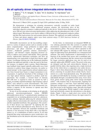
Coated side wall Gold + (a) (b)
SU-8
SU-8
TaN Resistor Si3N4 Mirror Ohmic contact
N -
I
GaAs P
GaP
Micro lens
Laser FIG. 4. Scanning electron microscope images of the final MEMS device a
Spring plate mirrors with surrounding spiral TaN resistors b A portion of
FIG. 2. Color online Cross-section schematic of a single pixel of the
the wafer fused GaAs–GaP PIN mesa array with patterned conductive SU-8.
device.
tops were then gold coated to form highly reflective mirrors.
ser beam on the GaAs photodetectors through the transparent This metal deposition was done at an angle to ensure that the
GaP back substrate. GaP was chosen as the support substrate sidewalls of an etched opening connecting the resistor side of
due to its high optical transparency to the control laser near the mirror to the front side, was also gold coated Fig. 3 v .
IR wavelength regime. The metal coated mirror top and PIN To fabricate the detector array, a GaAs wafer with epitaxi-
diode mesa act as the upper and lower electrodes of a capaci- ally grown p-i-n structure was bonded to a GaP substrate at
tive actuator, respectively. The generated photocurrent passes 700 ° C in a custom designed furnace and fixture Fig. 3 vi .
vertically through the semiconductive pillars causing a volt- The GaAs substrate was subsequently removed by a combi-
age drop across the thin film resistor in turn actuating the nation of lapping, polishing and wet etch. The transferred
mirror. p-i-n layers were then patterned and wet etched to form the
Figures 3 i –3 x illustrate the steps involved in fabricat- GaAs p-i-n mesas. The etch was monitored closely to stop in
ing the top mirror and bottom detector array. First, a low the half micron thick GaAs P region. A five layer Ni/Ge/Au/
stress plasma enhanced chemical vapor deposition recipe12 Ni/Au metal scheme was then deposited to form ohmic con-
was used to deposit 600 nm of silicon nitride on an indium tacts on the N side of each mesa and a single surrounding
phosphide InP substrate. The TaN sheet resistivity contact on the bottom P side Fig. 3 viii . In the final step, a
1.4 k / sq was then sputtered on lithographically pat- proprietary technique for doping and patterning SU-8 2010
terned photoresist AZ1512 and lifted off to form spiral resis- Microchem Corp. with a conductive polymer PANI was
tors Fig. 3 ii . Metal contact pads were then patterned fol- used to form two micron tall pillars on the mesas Fig. 3 ix .
lowing a similar process at the resistor ends Fig. 3 iii . Figure 4 shows the scanning electron microscope images of
Spring plates were then defined lithographically Fig. 3 iv portions of the final device with 900 pixels. The individual
in the center and a reactive ion etcher used to etch the Si3N4 pixel size including the resistor was 200 microns, with ac-
down to the InP. The actuators were then released by etching tual mirror area of 66 66 m2. The existing fill factor of
away the InP selectively using HCl. The released actuator 10% Fig. 4 a can be further improved by shrinking the
resistor size by using a higher resistivity material. The peri-
odicity of the p-i-n mesas and mirrors was 250 microns, and
Si3N4 GaP
the surrounding conductive SU-8 pillars were 10 m wide
InP GaAs PIN
(vi) Wafer fusion
Fig. 4 b .
TaN GaAs After fabricating the GaAs p-i-ns their breakdown and
Metal Doped SU-8 photoresponse characteristics were measured using a 830 nm
Photoresist laser source. As the photodetectors operate in series with the
patterned load resistor, their breakdown voltage sets an upper
(i) Si3N4 PECVD deposition (vii) Lapping and polishing limit on the resulting voltage drop across the actuator. Since
a voltage drop of 10 to 15 V is desirable across these actua-
tors, the p-i-ns were designed to have reverse breakdown
voltages in excess of 20 V. Figure 5 shows the I-V charac-
(ii) TaN sputtering (viii) Wet etch and metal deposition
100.0 3mW 830nm Laser
Back illumination through microlenses
Photocurrent (Microamps)
(iii) Resistor pads metal deposition (ix) Conductive SU-8 patterning 75.0 Top illumination after wafer fusion
Top illumination before wafer fusion
50.0 Dark
(iv) Si3N4 RIE etch (x) Samples cascaded
25.0
0.0
(v) Mirror release, metal deposition
0 10 20 30
Voltage (Volts)
FIG. 5. I-V curves illustrating the photo response of optically addressed
FIG. 3. Color online Micromirror and detector array fabrication steps. GaAs PINs before and after wafer fusion.
Downloaded 24 May 2010 to 129.63.234.140. Redistribution subject to AIP license or copyright; see http://apl.aip.org/apl/copyright.jsp
3. 211103-3 Mathur et al. Appl. Phys. Lett. 96, 211103 2010
830nm Laser
Frame grabber
LabVIEW
Dark Light
600
Oscilloscope
Iris
BS +
Mirror displacement (nm)
Photodiode
-
Device 400
He-Ne Laser
BS BS
200
Moving mirror
FIG. 6. Color online Interferometry and optical addressing setup for the
MEMS device beam splitter: BS .
0
teristics of the p-i-n diodes under no illumination dark , top 0 2 4 6
Optical power (mW)
illumination P-side on top before wafer fusion, and illumi-
nation through the GaP substrate P-side on bottom after FIG. 7. Interferograms showing fringe shift in shining light on the 2 M
resistor MEMS device inset . Mirror displacement vs optical intensity of
wafer fusion. A high photocurrent of about 80 A was ob- the MEMS device with 800 k resistors.
served on the first sample before wafer fusion on shining a 3
mW laser signal. The junction was found to deteriorate device, the TaN resistors were patterned to have a lower
slightly after the high temperature wafer fusion, and the pho- resistance of 800 k . The control laser intensity was var-
tocurrent dropped to 20 A when again addressed directly ied from 1–5 mW and the displacement measured in steps of
from the top. On the wafer fused test sample, the p-i-ns were quarter wavelengths = 632 nm as shown in Fig. 7. The
addressed through the GaP substrate and cascaded micro- mirror displacement was found to saturate close to 500 nm
lenses focal length 2 mm . The photocurrent further dropped corresponding to a 5 mW control laser power.
to 10 A due to additional optical losses , but was still In summary, a technique for optically addressing and
sufficient for actuation, provided a high value load resistor. actuating micromirrors using cascaded photodiodes has been
In the devices tested here, the TaN resistances were varied demonstrated. The device can be used as a simple ON/OFF
upto 2 M to ensure a voltage drop of at least 10 V across optical switch or as a phase corrector device in adaptive op-
the mirror. To monitor the mirror displacement as a function tics. The design proposed here offers several advantages over
of optical power, an inverted microscope was modified to other addressing techniques as it eliminates the need for
include standard interferometry as shown in Fig. 6. The complex circuitry, and may be adapted for several other ma-
MEMS device was then placed upside down and the micro- terial systems.
lens sample aligned carefully on top. A 830 nm Newport
LQA-830 control laser mounted on the microscope was then 1
L. Y. Lin, E. L. Goldstein, and R. W. Tkach, IEEE J. Sel. Top. Quantum
used to address approximately 100 photodiodes uniformly Electron. 5, 1 1999 .
2
and simultaneously via the microlenses. Note: The actual L. J. Hornbeck, White paper on DLP & MEMS technology, http://
power focused after the microlens on each individual detec- focus.ti.com/pdfs/dlpdmd/107_DLP_MEMS_Overview.pdf.
3
A. Tuantranont and V. M. Bright, IEEE J. Sel. Top. Quantum Electron. 8,
tor was not measured . A helium neon laser probe beam 632 33 2002 .
nm from a Michelson interferometer setup was focused on 4
H. Toshiyoshi and H. Fujita, J. Microelectromech. Syst. 5, 231 1996 .
5
an individual micromirror from under the microscope. The C. H. Ji and Y. K.Kim, J. Lightwave Technol. 21, 584 2003 .
6
reflected interference beam was captured using a frame grab- A. Jain, H. Qu, S. Todd, and H. Xie, Sens. Actuators, A 122, 9 2005 .
7
ber, and a portion of it reflected away using a beam splitter. J. M. Zanardi, P. O. Vaccaro, T. Fleischmann, T. Wang, K. Kubota, T.
Aida, T. Ohnishi, A. Sugimura, R. Izumoto, M. Hosoda, and S. Nashima,
An iris was then used to select only the innermost fringe Appl. Phys. Lett. 83, 3647 2003 .
from this reflected beam and focused on a photodetector. 8
J. E. Graebner, S. Pau, and P. L. Gammel, Appl. Phys. Lett. 81, 3531
Quantitative data on the mirror displacement was obtained 2002 .
9
by monitoring the intensity of this zeroth order fringe on an B. Haji-saeed, R. Kolluru, D. Pyburn, R. Leon, S. K. Sengupta, M. Testorf,
W. D. Goodhue, J. Khoury, A. Drehman, C. L. Woods, and J. Kierstead,
oscilloscope. The first device tested consisted of 2 M re-
Appl. Opt. 45, 2615 2006 .
sistors, and the mirror was found to displace abruptly even 10
J. Khoury, K. Vaccaro, C. L. Woods, B. Haji-saeed, S. K. Sengupta, C.
with very low intensity control laser signal 1 mW . This Armiento, W. D. Goodhue, J. Kierstead, and A. Davis, Proc. SPIE 6368,
can be attributed to a significant contribution to the total 11
636804 2006 .
parallel resistance by the semiconductive SU-8 posts, result- G. Griffith, B. Haji-saeed, S. K. Sengupta, W. D. Goodhue, J. Khoury, C.
L. Woods, and J. Kierstead, IEEE Photonics Technol. Lett. 19, 173
ing in a large voltage drop. The mirror operated as a simple 2007 .
ON/OFF switch in this case, as confirmed from the dark and 12
A. Tarraf, J. Daleiden, S. Irmer, D. Prasai, and H. Hillmer, J. Micromech.
light interferogram in the inset of Fig. 7. In our second test Microeng. 14, 317 2004 .
Downloaded 24 May 2010 to 129.63.234.140. Redistribution subject to AIP license or copyright; see http://apl.aip.org/apl/copyright.jsp