silicon ic fabrican technology
•Als PPT, PDF herunterladen•
12 gefällt mir•7,170 views

silicon IC fabrican technology

Empfohlen
Weitere ähnliche Inhalte
Was ist angesagt?
Was ist angesagt? (20)
Ähnlich wie silicon ic fabrican technology
Ähnlich wie silicon ic fabrican technology (20)
Kürzlich hochgeladen
Kürzlich hochgeladen (20)
silicon ic fabrican technology
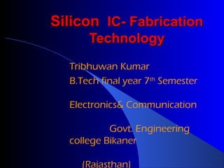
- 1. Silicon IC- Fabrication Technology Tribhuwan Kumar B.Tech final year 7th Semester Electronics& Communication Govt. Engineering college Bikaner (Rajasthan)
- 2. Silicon IC- Fabrication Technology To realize Semiconductor DEVICES or an INTEGRATED CIRCUIT an adequate set of technological steps is required that allows the realization of the same on top surface/plane of a semiconductor wafer.
- 3. Basic Steps of Si I.C-Fabrication: 1. 2. 3. 4. 5. Chemical Cleaning of Silicon Wafer Oxidation Photolithography Oxide Etching Diffusion Above steps are performed more than once depending on complexity of the I.C being fabricated. Subsequently, following steps are performed to accomplish the I.C fabrication. 6. Thin Film Metal Deposition 7. Photolithography 8. Metal etching 9. Annealing 10.Testing
- 4. P-N Junction Diode Circuit symbol Schematic diagram p-type net acceptor concentration NA n-type net donor concentration ND cross-sectional area AD ID + VD –
- 5. Practical P-N Junction Diode Structure ID + ID metal SiO2 For simplicity, assume that the doping profile changes abruptly at the junction. VD SiO2 p-type Si P-type n-type Si – metal
- 6. Fabrication of Silicon P-N Junction Diode 1. Chemical cleaning of silicon wafer 2. Oxidation 3. Photolithography 4. Silicon oxide etching 5. Diffusion 6. Thin film Metal (Aluminium) Deposition 7. Photolithography 8. Metal Etching 9. Semiconductor-Metal contact formation
- 7. Process Flow Chart for Fabrication of P-N Junction Si n-Silicon Chemically cleaned silicon wafer SiO2 Silicon dioxide Si n-Silicon Silicon-Oxide Interface Silicon Wafer with a Grown Silicon dioxide layer on top.
- 8. Silicon dioxide Positive Photo Resist Layer n-Silicon Spin Coat of Positive Photo Resist Ultra Violet Rays Glass plate Emulsion Silicon dioxide Mask U.V Exposed Region (Polymerized Photo Resist) n-Silicon Photo Resist Polymerization on U.V Exposure
- 9. Silicon dioxide Silicon dioxide n-Silicon Windows in Photo Resist After Development Silicon dioxide Silicon dioxide n-Silicon PR Coating on back of the wafer to protect oxide
- 10. Silicon dioxide n-Silicon Silicon Oxide ETCHING in BHF Silicon dioxide n-Silicon After Photo Resist & Wax removal Removal
- 11. PRE DEPOSITION Boron Atoms ambient Silicon dioxide Impurity Deposition (Boron/Phosphorous) n-Silicon Silicon dioxide n-Silicon Boro-silicate Glass and BORON Atoms
- 12. After Etching in Glass Etchant: Boron atoms Silicon dioxide n-Silicon
- 13. DRIVE - IN Silicon dioxide p p n-Silicon Silicon dioxide p n-Silicon p Pre-deposited wafer heated at High Temperature so impurity Move into silicon. Front coating photo resist layer
- 14. Silicon dioxide p p Back Oxide etching BHF p Photo resist removal n-Silicon Silicon dioxide p n-Silicon Dip in dil. HF to remove oxide if any on the front side and claen
- 15. Metal Contact Formation Silicon dioxide p p Aluminium Thin Film Deposition n-Silicon Silicon dioxide p n-Silicon Photo Resist Aluminium p
- 16. U. V Rays Glass Aluminium Silicoon dioxide p Photoresist p P- Contact n-Silicon PHOTOLITHOGRAPHY FOR Metal Contacts Silicon dioxide p p n-Silicon Development to remove U.V Exposed Photoresist
- 17. p Silicon dioxide p n-Silicon After Aluminium ETCHING p Silicon dioxide p n-Silicon Metal Thin Film Back Metal Contact Formation p One Diode Chip after separation of diode
- 18. Diodes chips are separated by scribing using a diamond point and packaged in a suiatable package as shown in the figure.
- 19. P-N Fabrication Training is Over