Hyper thread technology
•Als DOC, PDF herunterladen•
2 gefällt mir•1,233 views


Empfohlen
Weitere ähnliche Inhalte
Was ist angesagt?
Was ist angesagt? (20)
Ähnlich wie Hyper thread technology
Ähnlich wie Hyper thread technology (20)
Mehr von Shiva Krishna Chandra Shekar
Kürzlich hochgeladen
Kürzlich hochgeladen (20)
Hyper thread technology
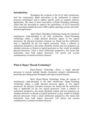
- 1. Introduction: Throughout the evolution of the IA-32 Intel Architecture, Intel has continuously added innovations to the architecture to improve processor performance and to address specific needs of compute intensive applications. The latest of these innovations is Hyper-Threading technology, which Intel has developed to improve the performance of IA-32 processors when executing multiple-processor (MP) capable operating systems and multi- threaded applications. Intel's Hyper-Threading Technology brings the concept of simultaneous multi-threading to the Intel Architecture. Hyper-Threading Technology makes a single physical processor appear as two logical processors; the physical execution resources are shared and the architecture state is duplicated for the two logical processors. From a software or architecture perspective, this means operating systems and user programs can schedule processes or threads to logical processors as they would on multiple physical processors. From a micro architecture perspective, this means that instructions from both logical processors will persist and execute simultaneously on shared execution resources. What is Hyper Thread Technology? Hyper-Thread Technology allows a single physical processor to execute multiple threads (instruction streams) simultaneously, potentially providing greater throughput and improved performance. Intel's Hyper-Thread Technology brings the concept of simultaneous multi-threading to the Intel Architecture. Hyper-Threading Technology makes a single physical processor appear as two logical processors; the physical execution resources are shared and the architecture state is duplicated for the two logical processors. From a software or architecture perspective, this means operating systems and user programs can schedule processes or threads to logical processors as they would on multiple physical processors. From a micro architecture perspective, this means that instructions from both logical processors will persist and execute simultaneously on shared execution resources.
- 2. Hyper Thread Technology Architecture: Hyper Thread Technology makes a single physical processor appear as multiple logical processors. To do this, there is one copy of the architecture state for each logical processor, and the logical processors share a single set of physical execution resources. From a software or architecture perspective, this means operating systems and user programs can schedule processes or threads to logical processors as they would on conventional physical processors in a multi-processor system. From a micro architecture perspective, this means that instructions from logical processors will persist and execute simultaneously on shared execution resources. Diagram In the above figure, a multiprocessor system with two physical processors those are not capable with Hyper Thread Technology. Diagram The above figure shows a multiprocessor system with tow physical processors that are Hyper Thread Technology capable. With two copies of the architectural state on each physical processor, the system appears to have four logical processors. The first implementation of Hyper Thread Technology is being made available on the Intel® Xeon™ processor family for dual and multiprocessor servers, with two logical processors per physical processor. By more efficiently using existing processor resources, the Intel Xeon processor family can significantly improve performance at virtually the same system cost. This implementation of Hyper Thread Technology added less than 5% to the relative chip size and maximum power requirements, but can provide performance benefits much greater than that. Each logical processor maintains a complete set of the architecture state. The architecture state consists of registers including the general-purpose registers, the control registers, the advanced programmable interrupt controller (APIC) registers, and some machine state registers. From a software perspective, once the architecture state is duplicated, the processor appears to be two processors. The number of transistors to store
- 3. the architecture state is an extremely small fraction of the total. Logical processors share nearly all other resources on the physical processor, such as caches, execution units, branch predictors, control logic, and buses. Each logical processor has its own interrupt controller or APIC. Interrupts sent to a specific logical processor are handled only by that logical processor. FIRST IMPLEMENTATION ON THE INTEL XEON PROCESSOR FAMILY Several goals were at the heart of the micro architecture design choices made for the Intel® XeonTM processor MP implementation of Hyper-Threading Technology. One goal was to minimize the die area cost of implementing Hyper-Threading Technology. Since the logical processors share the vast majority of micro architecture resources and only a few small structures were replicated, the die area cost of the first implementation was less than 5% of the total die area. A second goal was to ensure that when one logical processor is stalled the other logical processor could continue to make forward progress. A logical processor may be temporarily stalled for a variety of reasons, including servicing cache misses, handling branch miss predictions, or waiting for the results of previous instructions. Independent forward progress was ensured by managing buffering queues such that no logical processor can use all the entries when two active software threads2 were executing. This is accomplished by either partitioning or limiting the number of active entries each thread can have. A third goal was to allow a processor running only one active software thread to run at the same speed on a processor with Hyper- Threading Technology as on a processor without this capability. This means that partitioned resources should be recombined when only one software thread is active. A high-level view of the micro architecture pipeline is shown in Figure 4. As shown, buffering queues separate major pipeline logic blocks. The buffering queues are either partitioned or duplicated to ensure independent forward progress through each logic block.
- 4. Active software threads include the operating system idle loop because it runs a sequence of code that continuously checks the work queue(s). The operating system idle loop can consume considerable execution resources. Instruction Scheduling: The schedulers are at the heart of the out-of-order execution engine. Five uop schedulers are used to schedule different types of uops for the various execution units. Collectively, they can dispatch up to six uops each clock cycle. The schedulers determine when uops are ready to execute based on the readiness of their dependent input register operands and the availability of the execution unit resources. The memory instruction queue and general instruction queues send uops to the five scheduler queues as fast as they can, alternating between uops for the two logical processors every clock cycle, as needed. Each scheduler has its own scheduler queue of eight to twelve entries from which it selects uops to send to the execution units. The schedulers choose uops regardless of whether they belong to one logical processor or the other. The schedulers are effectively oblivious to logical processor distinctions. The uops are simply evaluated based on dependent inputs and availability of execution resources. For example, the schedulers could dispatch two uops from one logical processor and two uops from the other logical processor in the same clock cycle. To avoid deadlock and ensure fairness, there is a limit on the number of active entries that a logical processor can have in each scheduler's queue. This limit is dependent on the size of the scheduler queue. FRONT END: The front end of the pipeline is responsible for delivering instructions to the later pipe stages. Instructions generally come from the Execution Trace Cache (TC), which is the primary or Level 1 (L1) instruction cache. Figure 5b shows that only when there is a TC miss does the machine fetch and decode instructions from the integrated Level 2 (L2) cache. Near the TC is the Microcode ROM, which stores decoded instructions for the longer and more complex IA-32 instructions.
- 5. DIAGRAM Execution Trace Cache (TC): The TC stores decoded instructions, called micro-operations or "uops." Most instructions in a program are fetched and executed from the TC. Two sets of next-instruction-pointers independently track the progress of the two software threads executing. The two logical processors arbitrate access to the TC every clock cycle. If both logical processors want access to the TC at the same time, access is granted to one then the other in alternating clock cycles. For example, if one cycle is used to fetch a line for one logical processor, the next cycle would be used to fetch a line for the other logical processor, provided that both logical processors requested access to the trace cache. If one logical processor is stalled or is unable to use the TC, the other logical processor can use the full bandwidth of the trace cache, every cycle. The TC entries are tagged with thread information and are dynamically allocated as needed. The TC is 8-way set associative, and entries are replaced based on a least-recently-used (LRU) algorithm that is based on the full 8 ways. The shared nature of the TC allows one logical processor to have more entries than the other if needed. Microcode ROM: When a complex instruction is encountered, the TC sends a microcode-instruction pointer to the Microcode ROM. The Microcode ROM controller then fetches the uops needed and returns control to the TC. Two microcode instruction pointers are used to control the flows independently if both logical processors are executing complex IA-32 instructions. Both logical processors share the Microcode ROM entries. Access to the Microcode ROM alternates between logical processors just as in the TC.
- 6. ITLB and Branch Prediction: If there is a TC miss, then instruction bytes need to be fetched from the L2 cache and decoded into uops to be placed in the TC. The Instruction Translation Look a side Buffer (ITLB) receives the request from the TC to deliver new instructions, and it translates the next-instruction pointer address to a physical address. A request is sent to the L2 cache, and instruction bytes are returned. These bytes are placed into streaming buffers, which hold the bytes until they can be decoded. The ITLBs are duplicated. Each logical processor has its own ITLB and its own set of instruction pointers to track the progress of instruction fetch for the two logical processors. The instruction fetch logic in charge of sending requests to the L2 cache arbitrates on a first-come first- served basis, while always reserving at least one request slot for each logical processor. In this way, both logical processors can have fetches pending simultaneously. Each logical processor has its own set of two 64-byte streaming buffers to hold instruction bytes in preparation for the instruction decode stage. The ITLBs and the streaming buffers are small structures, so the die size cost of duplicating these structures is very low. The branch prediction structures are either duplicated or shared. The return stack buffer, which predicts the target of return instructions, is duplicated because it is a very small structure and the call/return pairs are better predicted for software threads independently. The branch history buffer used to look up the global history array is also tracked independently for each logical processor. However, the large global history array is a shared structure with entries that are tagged with a logical processor ID. SUPPORTING IA-32 PROCESSORS: An IA-32 processor with Hyper Thread Technology will appear to software as two independent IA-32 processors, similar to two physical processors in a traditional DP platform. This configuration allows operating system and application software that is already designed to run on a traditional DP or MP system to run unmodified on a platform that uses one or more IA-32 processors with Hyper Thread Technology. Here, the multiple threads that would be dispatched to two or more physical
- 7. processors are now dispatched to the logical processors in one or more IA- 32 processors with Hyper Thread Technology. At the firmware (BIOS) level, the basic procedures to initialize multiple processors with Hyper Thread Technology in an MP platform resemble closely those for a traditional MP platform4. An operating system designed to run on an traditional DP or MP platform can use the CPU-ID instruction to detect the presence of IA-32 processors with Hyper Thread Technology. The same mechanisms that are described in the multiprocessor specification version 1.4 to wake physical processors apply to the logical processors in an IA-32 with Hyper Thread Technology. Although existing operating system and application code will run correctly on a processor with Hyper Thread Technology, some relatively simple code modifications are recommended to get the optimum benefit from Hyper Thread Technology. IMPLEMENTATION OF IA-32 PROCESSORS: IA-32 Instruction Decode: IA-32 instructions are cumbersome to decode because the instructions have a variable number of bytes and have many different options. A significant amount of logic and intermediate state is needed to decode these instructions. Fortunately, the TC provides most of the uops, and decoding is only needed for instructions that miss the TC. The decode logic takes instruction bytes from the streaming buffers and decodes them into uops. When both threads are decoding instructions simultaneously, the streaming buffers alternate between threads so that both threads share the same decoder logic. The decode logic has to keep two copies of all the state needed to decode IA-32 instructions for the two logical processors even though it only decodes instructions for one logical processor at a time. In general, several instructions are decoded for one logical processor before switching to the other logical processor. The decision to do a coarser level of granularity in switching between logical processors was made in the interest of die size and to reduce complexity. Of course, if only one logical processor needs the decode logic, the full decode bandwidth is dedicated to that logical processor. The decoded instructions are written into the TC and forwarded to the uop queue.
- 8. Uop Queue: After uops are fetched from the trace cache or the Microcode ROM, or forwarded from the instruction decode logic, they are placed in a "uop queue." This queue decouples the Front End from the Out-of-order Execution Engine in the pipeline flow. The uop queue is partitioned such that each logical processor has half the entries. This partitioning allows both logical processors to make independent forward progress regardless of front- end stalls (e.g., TC miss) and execution stalls. OUT-OF-ORDER EXECUTION ENGINE: The out-of-order execution engine consists of the allocation, register renaming, scheduling, and execution functions, as shown in Figure 6. This part of the machine re-orders instructions and executes them as quickly as their inputs are ready, without regard to the original program order. Allocator: The out-of-order execution engine has several buffers to perform its re-ordering, tracing, and sequencing operations. The allocator logic takes uops from the uop queue and allocates many of the key machine buffers needed to execute each uop, including the 126 re-order buffer entries, 128 integer and 128 floating-point physical registers, 48 load and 24 store buffer entries. Some of these key buffers are partitioned such that each logical processor can use at most half the entries. Specifically, each logical processor can use up to a maximum of 63 re-order buffer entries, 24 load buffers, and 12 store buffer entries. If there are uops for both logical processors in the uop queue, the allocator will alternate selecting uops from the logical processors every clock cycle to assign resources. If a logical processor has used its limit of a needed resource, such as store buffer entries, the allocator will signal "stall" for that logical processor and continue to assign resources for the other logical processor. In addition, if the uop queue only contains uops for one logical processor, the allocator will try to assign resources for that logical processor every cycle to optimize allocation bandwidth, though the resource limits would still be enforced.
- 9. By limiting the maximum resource usage of key buffers, the machine helps enforce fairness and prevents deadlocks. Register Rename: The register rename logic renames the architectural IA-32 registers onto the machine's physical registers. This allows the 8 general-use IA-32 integer registers to be dynamically expanded to use the available 128 physical registers. The renaming logic uses a Register Alias Table (RAT) to track the latest version of each architectural register to tell the next instruction(s) where to get its input operands. Since each logical processor must maintain and track its own complete architecture state, there are two RATs, one for each logical processor. The register renaming process is done in parallel to the allocator logic described above, so the register rename logic works on the same uops to which the allocator is assigning resources. Once uops have completed the allocation and register rename processes, they are placed into two sets of queues, one for memory operations (loads and stores) and another for all other operations. The two sets of queues are called the memory instruction queue and the general instruction queue, respectively. The two sets of queues are also partitioned such that uops from each logical processor can use at most half the entries. Execution Units: The execution core and memory hierarchy are also largely oblivious to logical processors. Since the source and destination registers were renamed earlier to physical registers in a shared physical register pool, uops merely access the physical register file to get their destinations, and they write results back to the physical register file. Comparing physical register numbers enables the forwarding logic to forward results to other executing uops without having to understand logical processors. After execution, the uops are placed in the re-order buffer. The re-order buffer decouples the execution stage from the retirement stage. The re-order buffer is partitioned such that each logical processor can use half the entries.
- 10. Retirement: Uop retirement logic commits the architecture state in program order. The retirement logic tracks when uops from the two logical processors are ready to be retired, then retires the uops in program order for each logical processor by alternating between the two logical processors. Retirement logic will retire uops for one logical processor, then the other, alternating back and forth. If one logical processor is not ready to retire any uops then all retirement bandwidth is dedicated to the other logical processor. Once stores have retired, the store data needs to be written into the level-one data cache. Selection logic alternates between the two logical processors to commit store data to the cache. MEMORY SUBSYSTEM: The memory subsystem includes the DTLB, the low-latency Level 1 (L1) data cache, the Level 2 (L2) unified cache, and the Level 3 unified cache (the Level 3 cache is only available on the Intel® XeonTM processor MP). Access to the memory subsystem is also largely oblivious to logical processors. The schedulers send load or store uops without regard to logical processors and the memory subsystem handles them as they come. DTLB: The DTLB translates addresses to physical addresses. It has 64 fully associative entries; each entry can map either a 4K or a 4MB page. Although the DTLB is a shared structure between the two logical processors, each entry includes a logical processor ID tag. Each logical processor also has a reservation register to ensure fairness and forward progress in processing DTLB misses. L1 Data Cache, L2 Cache, L3 Cache: The L1 data cache is 4-way set associative with 64-byte lines. It is a write-through cache, meaning that writes are always copied to the L2 cache. The L1 data cache is virtually addressed and physically tagged.
- 11. The L2 and L3 caches are 8-way set associative with 128-byte lines. The L2 and L3 caches are physically addressed. Both logical processors, without regard to which logical processor's uops may have initially brought the data into the cache, can share all entries in all three levels of cache. Because logical processors can share data in the cache, there is the potential for cache conflicts, which can result in lower observed performance. However, there is also the possibility for sharing data in the cache. For example, one logical processor may prefetch instructions or data, needed by the other, into the cache; this is common in server application code. In a producer-consumer usage model, one logical processor may produce data that the other logical processor wants to use. In such cases, there is the potential for good performance benefits. BUS: Logical processor memory requests not satisfied by the cache hierarchy are serviced by the bus logic. The bus logic includes the local APIC interrupt controller, as well as off-chip system memory and I/O space. Bus logic also deals with cacheable address coherency (snooping) of requests originated by other external bus agents, plus incoming interrupt request delivery via the local APICs. From a service perspective, requests from the logical processors are treated on a first-come basis, with queue and buffering space appearing shared. Priority is not given to one logical processor above the other. Distinctions between requests from the logical processors are reliably maintained in the bus queues nonetheless. Requests to the local APIC and interrupt delivery resources are unique and separate per logical processor. Bus logic also carries out portions of barrier fence and memory ordering operations, which are applied to the bus request queues on a per logical processor basis. For debug purposes, and as an aid to forward progress mechanisms in clustered multiprocessor implementations, the logical processor ID is visibly sent onto the processor external bus in the request phase portion of a transaction. Other bus transactions, such as cache line
- 12. eviction or prefetch transactions, inherit the logical processor ID of the request that generated the transaction SINGLE-TASK AND MULTI-TASK MODES: To optimize performance when there is one software thread to execute, there are two modes of operation referred to as single-task (ST) or multi-task (MT). In MT-mode, there are two active logical processors and some of the resources are partitioned as described earlier. There are two flavors of ST-mode: single-task logical processor 0 (ST0) and single-task logical processor 1 (ST1). In ST0- or ST1-mode, only one logical processor is active, and resources that were partitioned in MT-mode are re-combined to give the single active logical processor use of all of the resources. The IA- 32 Intel Architecture has an instruction called HALT that stops processor execution and normally allows the processor to go into a lower-power mode. HALT is a privileged instruction, meaning that only the operating system or other ring-0 processes may execute this instruction. User-level applications cannot execute HALT. On a processor with Hyper-Threading Technology, executing HALT transitions the processor from MT-mode to ST0- or ST1-mode, depending on which logical processor executed the HALT. For example, if logical processor 0 executes HALT, only logical processor 1 would be active; the physical processor would be in ST1-mode and partitioned resources would be recombined giving logical processor 1 full use of all processor resources. If the remaining active logical processor also executes HALT, the physical processor would then be able to go to a lower-power mode. In ST0- or ST1-modes, an interrupt sent to the Halted processor would cause a transition to MT-mode. The operating system is responsible for managing MT-mode transitions (described in the next section). The Intel® XeonTM processor family delivers the highest server system performance of any IA-32 Intel architecture processor introduced to date. Initial benchmark tests show up to a 65% performance increase on high-end server applications when compared to the previous-generation Pentium® III Xeon™ processor on 4-way server platforms. A significant portion of those gains can be attributed to Hyper-Threading Technology.
- 13. DIAGRAM The online transaction processing performance, scaling from a single-processor configuration through to a 4-processor system with Hyper- Threading Technology enabled. This graph is normalized to the performance of the single-processor system. It can be seen that there is a significant overall performance gain attributable to Hyper-Threading Technology, 21% in the cases of the single and dual-processor systems. The benefit of Hyper-Threading Technology when executing other server-centric benchmarks. The workloads chosen were two different benchmarks that are designed to exercise data and Web server characteristics and a workload that focuses on exercising a server-side Java environment. In these cases the performance benefit ranged from 16 to 28%. All the performance results quoted above are normalized to ensure that readers focus on the relative performance and not the absolute performance. Performance tests and ratings are measured using specific computer systems and/or components and reflect the approximate performance of Intel products as measured by those tests. Any difference in system hardware or software design or configuration may affect actual performance. Buyers should consult other sources of information to evaluate the performance of systems or components they are considering purchasing. Hyper Thread Technology and Windows Streams: Windows-based servers receive processor information from the BIOS. Each server vendor creates their own BIOS using specifications provided by Intel. Assuming the BIOS is written according to Intel specifications, it begins counting processors using the first logical processor on each physical processor. Once it has counted a logical processor on all of the physical processors, it will count the second logical processor on each physical processor, and so on.
- 14. Numbers indicate the order in which logical processors are recognised by BIOS when written according to the Intel specifications. This diagram shows a four way system enabled with Hyper Thread Technology. It is critical that the BIOS count logical processors in the manner described; otherwise, Windows 2000 or its applications may use logical processors when they should be using physical processors instead. For example, consider an application that is licensed to use two processors on the system diagrammed above. Such an application will achieve better performance using two separate physical processors than it would use two logical processors on the same physical processor. CONCLUSION: Intel’s Hyper Thread Technology brings the concept of simultaneous multi-threading to the Intel Architecture. This is a significant new technology direction for Intel’s future processors. It will be become increasingly important going forward as it adds a new technique for obtaining additional performance for lower transistor and power costs. The first implementation of Hyper Thread Technology was done on the Intel® Xeon™ processor MP. In this implementation there are two logical processors on each physical processor. The logical processors have their own independent architecture state, but they share nearly all the physical execution and hardware resources of the processor. The goal was to implement the technology at minimum cost while ensuring forward progress on logical processors, even if the other is stalled, and to deliver full 1 5 2 6 3 7 4 8 Logical processors Physical Processors
- 15. performance even when there is only one active logical processor. These goals were achieved through efficient logical processor selection algorithms and the creative partitioning and recombining algorithms of many key resources. Measured performance on the Intel Xeon processor MP with Hyper Thread Technology shows performance gains of up to 30% on common server application benchmarks for this technology. The potential of Hyper Thread Technology is tremendous; our current implementation has only just begun to tap into this potential. Hyper Thread Technology is expected to be viable from mobile processors to servers; its introduction into market segments other than server is only gated by the availability and prevalence of threaded applications and workloads in those markets.
- 16. Hyper-Threading Technology is a groundbreaking innovation from Intel® Corporation that enables multi-threaded software applications to execute threads in parallel. This level of threading technology has never been seen before in a general-purpose microprocessor. Internet, e-Business, and enterprise software applications continue to put higher demands on processors. To improve performance in the past, threading was enabled in the software by splitting instructions into multiple streams so that multiple processors could act upon them. Today with Hyper-Threading Technology, processor-level threading can be utilized which offers more efficient use of processor resources for greater parallelism and improved performance on today’s multi-threaded software. Hyper-Threading Technology provides thread-level-parallelism (TLP) on each processor resulting in increased utilization of processor execution resources. As a result, resource utilization yields higher processing throughput. Hyper- Threading Technology is a form of simultaneous multi-threading technology (SMT) where multiple threads of software applications can be run simultaneously on one processor. This is achieved by duplicating the architectural state on each processor, while sharing one set of processor execution resources. Hyper- Threading Technology also delivers faster response times for multi-tasking workload environments. By allowing the processor to use on-die resources that would otherwise have been idle, Hyper-Threading Technology provides a performance boost on multi-threading and multi-tasking operations for the Intel® NetBurst™ micro architecture. This technology is largely invisible to the platform. In fact, many applications are already multi-threaded and will automatically benefit from this technology. However, multi-threaded applications take full advantage of the increased performance that Hyper-Threading Technology has to offer, allowing users will see immediate performance gains when multitasking. Today`s multi-processing aware software is also compatible with Hyper-Threading Technology enabled platforms, but further performance gains can be realized by specifically tuning software for Hyper-Threading Technology. This technology complements traditional multi-processing by providing additional headroom for future software optimizations and business growth. Hyper-Threading Technology offers many benefits to e-Business and the enterprise such as: Enables more user support improving business productivity Provides faster response times for Internet and e-Business applications enhancing customer experience Increases number of transactions that can be processed Allows compatibility with existing IA-32 applications and operating systems Handles larger workloads Offers headroom for future business growth and new solution capabilities