SlideShare ist ein Scribd-Unternehmen logo
1 von 13
Downloaden Sie, um offline zu lesen
Question: What is P-N junction? Explain the formation of potential barrier and depletion layer? With
no external voltage.

A p–n junction is a junction formed by joining p-type and n-type semiconductors together in very close
contact. The term junction refers to the boundary interface where the two regions of the semiconductor
meet. If they were constructed of two separate pieces this would introduce a grain boundary, so p–n
junctions are more often created in a single crystal of semiconductor by doping, for example by ion
implantation, diffusion of dopants, or by epitaxy (growing a layer of crystal doped with one type of
dopant on top of a layer of crystal doped with another type of dopant).

Formation of the Depletion Region.

At the instant of the PN junction formation free electrons near the junction diffuse across the junction
into the P region and combine with holes.


Filling a hole makes a negative ion and leaves behind a positive ion on the N side.

These two layers of positive and negative charges form the depletion region, as the region near the
junction is depleted of charge carriers.

As electrons diffuse across the junction a point is reached where the negative charge repels any further
diffusion of electrons.

The depletion region now acts as a barrier.

Barrier Potential.


The electric field formed in the depletion region acts as a barrier.

External energy must be applied to get the electrons to move across the barrier of the electric field.

The potential difference required to move the electrons through the electric field is called the barrier
potential.
Barrier potential of a PN junction depends on the type of semiconductor material, amount of doping and
temperature.

This is approximately 0.7V for silicon and 0.3V for germanium.


Question: Draw the energy level diagram of a PN junction and explain how a junction barrier is
developed across an unbiased junction.

Energy Diagrams of PN Junction:


The valence band and conduction band in N-Type material are slightly lower than that of P-Type
material.


As diffusion occurs the depletion region forms and the energy level of the N region conduction band
drops, causing alignment of the top of the N region conduction band and the bottom of the P region
conduction band. At this point the energy bands are at equilibrium.


There is an energy gradient across the depletion region that a N region electron must climb to get to the
P region.

Biasing the PN Junction.


Forward Bias.

An external D.C. voltage is applied to a PN junction to bias it.

Forward bias allows current through a PN junction.
Bias voltage imparts sufficient energy to the free electrons so they overcome the barrier potential and
move into the P region.


Conduction occurs with electron current in the N-Type material and hole current in the P-Type material.

As more electrons and holes flow in the depletion region the number of positive and negative ions is
reduced, causing the depletion region to narrow.

The energy loss in overcoming the barrier potential results in a voltage drop across the PN junction
equal to the barrier potential.

( 0.7V for Si, 0.3V for Ge.)

When a PN junction is forward biased the N region conduction band is raised to a higher level that
overlaps with the P region conduction band.
Reverse Bias


Reverse bias prevents current flow through a PN junction.

                                 P                        N


Reverse bias potential attracts the majority carriers away from the PN junction widening the depletion
region.

The potential across the depletion region is equal to the bias voltage.

Reverse current can flow through the PN junction due to minority carriers.

When a PN junction is reverse biased the energy hill increases.


Reverse Breakdown.

If the reverse bias voltage is increased to the breakdown voltage, the reverse current will drastically
increase.

This is due to collisions of fast minority carriers with atoms, knocking out valence electrons. This process
avalanches and results in a high reverse current damaging the PN structure.
Question: Explain the majority & minority carriers produces in n-type & t-type materials.

Majority and Minority Carriers: In the intrinsic state, the number of free electrons in Ge or Si is due only
to those few electrons in the valence band that have acquired sufficient energy from thermal or light
sources to break the covalent bond or to the few impurities that could not be re-moved. The vacancies
left behind in the covalent bonding structure represent our very limited supply of holes. In an n-type
material, the number of holes has not changed significantly from this intrinsic level. The net result,
therefore, is that the number of electrons far outweighs the number of holes. For this reason In an n-
type material (Fig. 1.13a) the electron is called the majority carrier and the hole the minority carrier. For
the p-type material the number of holes far outweighs the number of electrons, as shown in Fig. 1.13b.
Therefore: In a p-type material the hole is the majority carrier and the electron is the minority carrier.
When the fifth electron of a donor atom leaves the parent atom, the atom remaining acquires a net
positive charge: hence the positive sign in the donor-ion representation. For similar reasons, the
negative sign appears in the acceptor ion. The n- and p-type materials represent the basic building
blocks of semiconductor devices. We will find in the next section that the “joining “of a single n-type
material with a p-type material will result in a semiconductor element of considerable importance in
electronic systems.


Question: What is forward biasing & reverse biasing? Explain the PN Junction forward bias & reverse
bias.

Forward biasing: Forward bias occurs when the P-type semiconductor material is connected to the
positive terminal of a battery and the N-type semiconductor material is connected to the negative
terminal, as shown below. This usually makes the p–n junction conduct.

With a battery connected this way, the holes in the P-type region and the electrons in the N-type
region are pushed towards the junction. This reduces the width of the depletion zone. The
positive charge applied to the P-type material repels the holes, while the negative charge applied
to the N-type material repels the electrons. As electrons and holes are pushed towards the
junction, the distance between them decreases. This lowers the barrier in potential. With
increasing forward-bias voltage, the depletion zone eventually becomes thin enough that the
zone's electric field can't counteract charge carrier motion across the p–n junction, consequently
reducing electrical resistance. The electrons which cross the p–n junction into the P-type material
(or holes which cross into the N-type material) will diffuse in the near-neutral region. Therefore,
the amount of minority diffusion in the near-neutral zones determines the amount of current that may flow
through the diode.

Only majority carriers (electrons in N-type material or holes in P-type) can flow through a semiconductor
for a macroscopic length. With this in mind, consider the flow of electrons across the junction. The
forward bias causes a force on the electrons pushing them from the N side toward the P side. With
forward bias, the depletion region is narrow enough that electrons can cross the junction and inject into
the P-type material. However, they do not continue to flow through the P-type material indefinitely,
because it is energetically favorable for them to recombine with holes. The average length an electron
travels through the P-type material before recombining is called the diffusion length, and it is typically on
the order of microns.

Although the electrons penetrate only a short distance into the P-type material, the electric current
continues uninterrupted, because holes (the majority carriers) begin to flow in the opposite direction. The
total current (the sum of the electron and hole currents) is constant in space, because any variation would
cause charge buildup over time (this is Kirchhoff's current law). The flow of holes from the P-type region
into the N-type region is exactly analogous to the flow of electrons from N to P (electrons and holes swap
roles and the signs of all currents and voltages are reversed).

Therefore, the macroscopic picture of the current flow through the diode involves electrons flowing
through the N-type region toward the junction, holes flowing through the P-type region in the opposite
direction toward the junction, and the two species of carriers constantly recombining in the vicinity of the
junction. The electrons and holes travel in opposite directions, but they also have opposite charges, so the
overall current is in the same direction on both sides of the diode, as required.

Reverse Bias: Reverse biased usually refers to how a diode is used in a circuit. If a diode is
reverse biased, the voltage at the cathode is higher than that at the anode. Therefore, no current
will flow until the diode breaks down. Connecting the P-type region to the negative terminal of
the battery and the N-type region to the positive terminal, corresponds to reverse bias. The
connections are illustrated in the following diagram:


Because the p-type material is now connected to the negative terminal of the power supply, the
'holes' in the P-type material are pulled away from the junction, causing the width of the
depletion zone to increase. Similarly, because the N-type region is connected to the positive
terminal, the electrons will also be pulled away from the junction. Therefore the depletion region
widens, and does so increasingly with increasing reverse-bias voltage. This increases the voltage
barrier causing a high resistance to the flow of charge carriers thus allowing minimal electric
current to cross the p–n junction.

The strength of the depletion zone electric field increases as the reverse-bias voltage increases.
Once the electric field intensity increases beyond a critical level, the p–n junction depletion zone
breaks-down and current begins to flow, usually by either the Zener or avalanche breakdown
processes. Both of these breakdown processes are non-destructive and are reversible, so long as
the amount of current flowing does not reach levels that cause the semiconductor material to
overheat and cause thermal damage.

This effect is used to one's advantage in zener diode regulator circuits. Zener diodes have a
certain - low - breakdown voltage. A standard value for breakdown voltage is for instance 5.6V.
This means that the voltage at the cathode can never be more than 5.6V higher than the voltage
at the anode, because the diode will break down - and therefore conduct - if the voltage gets any
higher. This effectively regulates the voltage over the diode.

Another application where reverse biased diodes are used is in Varicap diodes. The width of the
depletion zone of any diode changes with voltage applied. This varies the capacitance of the
diode. For more information, refer to the Varicap article.

Question: What is break down? Explain zener break down and avalence break down?


A Zener diode is a type of diode that permits current not only in the forward direction like a
normal diode, but also in the reverse direction if the voltage is larger than the breakdown voltage
known as "Zener knee voltage" or "Zener voltage". The device was named after Clarence Zener,
who discovered this electrical property.

A conventional solid-state diode will not allow significant current if it is reverse-biased below its
reverse breakdown voltage. When the reverse bias breakdown voltage is exceeded, a
conventional diode is subject to high current due to avalanche breakdown. Unless this current is
limited by external circuitry, the diode will be permanently damaged. In case of large forward
bias (current in the direction of the arrow), the diode exhibits a voltage drop due to its junction
built-in voltage and internal resistance. The amount of the voltage drop depends on the
semiconductor material and the doping concentrations.

A Zener diode exhibits almost the same properties, except the device is specially designed so as
to have a greatly reduced breakdown voltage, the so-called Zener voltage. By contrast with he
conventional device, a reverse-biased Zener diode will exhibit a controlled breakdown and allow
the current to keep the voltage across the Zener diode at the Zener voltage. For example, a diode
with a Zener breakdown voltage of 3.2 V will exhibit a voltage drop of 3.2 V if reverse bias
voltage applied across it is more than its Zener voltage. The Zener diode is therefore ideal for
applications such as the generation of a reference voltage (e.g. for an amplifier stage), or as a
voltage stabilizer for low-current applications.
The Zener diode's operation depends on the heavy doping of its p-n junction allowing electrons
to tunnel from the valence band of the p-type material to the conduction band of the n-type
material. In the atomic scale, this tunneling corresponds to the transport of valence band
electrons into the empty conduction band states; as a result of the reduced barrier between these
bands and high electric fields that are induced due to the relatively high levels of dopings on both
sides.The breakdown voltage can be controlled quite accurately in the doping process. While
tolerances within 0.05% are available, the most widely used tolerances are 5% and 10%.
Breakdown voltage for commonly available zener diodes can vary widely from 1.2 volts to 200
volts.

Another mechanism that produces a similar effect is the avalanche effect as in the avalanche
diode. The two types of diode are in fact constructed the same way and both effects are present
in diodes of this type. In silicon diodes up to about 5.6 volts, the Zener effect is the predominant
effect and shows a marked negative temperature coefficient. Above 5.6 volts, the avalanche
effect becomes predominant and exhibits a positive temperature coefficient. In a 5.6 V diode, the
two effects occur together and their temperature coefficients neatly cancel each other out, thus
the 5.6 V diode is the component of choice in temperature-critical applications. Modern
manufacturing techniques have produced devices with voltages lower than 5.6 V with negligible
temperature coefficients, but as higher voltage devices are encountered, the temperature
coefficient rises dramatically. A 75 V diode has 10 times the coefficient of a 12 V diode.

All such diodes, regardless of breakdown voltage, are usually marketed under the umbrella term
of "Zener diode".

Avalanche breakdown: avalanche breakdown is a phenomenon that can occur in both
insulating and semiconducting materials. It is a form of electric current multiplication that can
allow very large currents to flow within materials which are otherwise good insulators. It is a
type of electron avalanche.

Explanation: Materials conduct electricity if they contain mobile charge carriers. There are two
types of charge carrier in a semiconductor: free electrons and electron holes. A fixed electron in
a reverse-biased diode may break free due to its thermal energy, creating an electron-hole pair. If
there is a voltage gradient in the semiconductor, the electron will move towards the positive
voltage while the hole will "move" towards the negative voltage. Most of the time, the electron
and hole will just move to opposite ends of the crystal and stop. Under the right circumstances,
however, (ie. when the voltage is high enough) the free electron may move fast enough to knock
other electrons free, creating more free-electron-hole pairs (ie. more charge carriers), increasing
the current. Fast-"moving" holes may also result in more electron-hole pairs being formed. In a
fraction of a nanosecond, the whole crystal begins to conduct quite nicely.

Avalanche breakdown usually destroys regular diodes, but avalanche diodes are designed to
break down this way at low voltages and can survive the reverse current.

The voltage at which the breakdown occurs is called the breakdown voltage. Once avalanche
breakdown has occurred, the material will continue to conduct if the voltage across it drops
below the breakdown voltage. This is different from a Zener diode because a Zener diode will
stop conducting once the reverse voltage drops below the breakdown voltage.
Question: What is knee voltage?

The point or area on a graph of diode current versus voltage where the forward current suddenly
increases. It is approximately equal to the barrier potential of the diode.


Question: Explain V-I Characteristics of P-N junction.

Forward biasing: A p-n junction is said to be forward biased, if the positive terminal of the external battery B is
connected to p-side and the negative terminal to the n-side of the p-n junction. Here the forward bias opposes the
potential barrier VB and so the depletion layer becomes thin. The majority charge carriers in the P type and N types
are repelled by their respective terminals due to battery B and hence cross the junction. On crossing the junction,
recombination process takes place. For every electron hole combination, a covalent bond near the +ve terminal of
the battery B is broken and this liberates an electron which enters the +ve terminal of B through connecting wires.
This in turn creates more holes in P-region. At the other end, the electrons from -ve terminal of B enter n-region to
replace electron lost due to recombination process. Thus a large current will flow to migration of majority carriers
across the p-n junction which is called forward current.

Reverse biasing: A p-n junction is said to be reverse biased if the positive terminal of the battery B is connected to
N-side and the negative terminal to p-side of the p-n junction. The majority carriers are pulled away from the
junction and the depletion region becomes thick. The resistance becomes high when reverse biased and so there is
no conduction across the junction due to majority carriers. The minority carriers however cross the junction and
they constitute a current that flows in the opposite direction. This is the reverse current.

The V-I characteristics of a p-n junction diode
Question: What are LED? How do they works? Explain Briefly, mention some of it’s application.

A light-emitting diode (LED) is a semiconductor light source. LEDs are used as indicator lamps in many
devices, and are increasingly used for lighting. Introduced as a practical electronic component in
1962,[2] early LEDs emitted low-intensity red light, but modern versions are available across the visible,
ultraviolet and infrared wavelengths, with very high brightness.

The LED is based on the semiconductor diode. When a diode is forward biased (switched on), electrons
are able to recombine with holes within the device, releasing energy in the form of photons. This effect
is called electroluminescence and the color of the light (corresponding to the energy of the photon) is
determined by the energy gap of the semiconductor. An LED is usually small in area (less than 1 mm2),
and integrated optical components are used to shape its radiation pattern and assist in reflection.[3]
LEDs present many advantages over incandescent light sources including lower energy consumption,
longer lifetime, improved robustness, smaller size, faster switching, and greater durability and reliability.
However, they are relatively expensive and require more precise current and heat management than
traditional light sources. Current LED products for general lighting are more expensive to buy than
fluorescent lamp sources of comparable output. They also enjoy use in applications as diverse as
replacements for traditional light sources in automotive lighting (particularly indicators) and in traffic
signals. The compact size of LEDs has allowed new text and video displays and sensors to be developed,
while their high switching rates are useful in advanced communications technology.

Application of LEDs fall into three major categories:

       Visual signal application where the light goes more or less directly from the LED to the human
        eye, to convey a message or meaning.
       Illumination where LED light is reflected from object to give visual response of these objects.
       Generate light for measuring and interacting with processes that do not involve the human
        visual system.

Question: How an ideal diode acts as a switch?

    The IDEAL DIODE serves as an electrical one-way valve. It conducts current much more
readily in one direction, called the FORWARD (BIAS) DIRECTION, than it does in the other
direction called the REVERSE (BIAS) DIRECTION.

        IDEAL DIODE acts like a SWITCH that closes to allow current flow in the forward
direction but opens to prevent current flow in the reverse direction.
Question: What is rectifier and rectification?

Rectifier: Rectifier is an electrical device which can change an a.c current to d.c current.

Rectification: The process of changes ac to d.c is called rectification.

Question : What is half wave rectifier? Explain the use of a PN junction diode as a half wave rectifier?
Find out the efficiency & ripple factor of a half wave rectifier?

In half wave rectification, either the positive or negative half of the AC wave is passed, while the other
half is blocked. Because only one half of the input waveform reaches the output, it is very inefficient if
used for power transfer. Half-wave rectification can be achieved with a single diode in a one-phase
supply, or with three diodes in a three-phase supply.


    •   Average value of the output voltage, Vdc

    •   Average value of the output current, Idc

    •   Output dc power, Pdc

            –    Pdc = VdcIdc

    •   rms value of the output voltage, Vrms

    •   Output ac power, Pac

            –    Pac = VrmsIrms

    •   Efficiency, η

            –    η = Pdc/Pac

    •   Effective (rms) value of the ac component of the output voltage, Vac

            –    Vac = Vrms2 – Vdc2

    •   Form factor, FF

            –    FF = Vrms/Vdc

    •   Ripple factor, RF
–   RF = Vac/Vdc

   •   Alternate form for ripple factor

   •   Transformer utilization factor, TUF

           –   TUF = Pdc/VsIs

           –   Vs, Is are rms voltage and current of the transformer secondary

Determine the Average Voltage, Vdc
.

Weitere ähnliche Inhalte

Was ist angesagt?

Physics project class 12
Physics project class 12Physics project class 12
Physics project class 12Pranav12109
 
PN JUNCTION DIODE IN हिंदी|FORWARD AND REVERSE BIASED OF DIODE|BASIC ELECTRON...
PN JUNCTION DIODE IN हिंदी|FORWARD AND REVERSE BIASED OF DIODE|BASIC ELECTRON...PN JUNCTION DIODE IN हिंदी|FORWARD AND REVERSE BIASED OF DIODE|BASIC ELECTRON...
PN JUNCTION DIODE IN हिंदी|FORWARD AND REVERSE BIASED OF DIODE|BASIC ELECTRON...Prasant Kumar
 
Physics investigatory projec tdocx
Physics investigatory projec tdocxPhysics investigatory projec tdocx
Physics investigatory projec tdocxHrithiksingla
 
Physics Investigatory:To Study V-I Characteristics Of Zener Diode
Physics Investigatory:To Study V-I Characteristics Of Zener DiodePhysics Investigatory:To Study V-I Characteristics Of Zener Diode
Physics Investigatory:To Study V-I Characteristics Of Zener DiodeGautammaini9
 
Rectifier class 12th physics investigatory project
Rectifier class 12th physics investigatory projectRectifier class 12th physics investigatory project
Rectifier class 12th physics investigatory projectndaashishk7781
 
physics investigatory project for class 12th students
 physics investigatory project for class 12th students physics investigatory project for class 12th students
physics investigatory project for class 12th studentsGaurav Jha
 
Pn junction diode class 12 investegatory project
Pn junction diode class 12 investegatory projectPn junction diode class 12 investegatory project
Pn junction diode class 12 investegatory projectabhijeet singh
 
Physics Project for class 12 isc Junction and diode
Physics Project for class 12 isc Junction and diodePhysics Project for class 12 isc Junction and diode
Physics Project for class 12 isc Junction and diodeIshani gupta Gupta
 
CLASS 12 PHYSICS PROJECT - Measuring current using halfwave rectifier
CLASS 12 PHYSICS PROJECT - Measuring current using halfwave rectifierCLASS 12 PHYSICS PROJECT - Measuring current using halfwave rectifier
CLASS 12 PHYSICS PROJECT - Measuring current using halfwave rectifierMathesh T
 
physics cbse 12th classs investigatory project
physics cbse 12th classs investigatory projectphysics cbse 12th classs investigatory project
physics cbse 12th classs investigatory projectVishvjeet Yadav
 
Pn junction diode by sarmad baloch
Pn junction diode by sarmad balochPn junction diode by sarmad baloch
Pn junction diode by sarmad balochSarmad Baloch
 
PHYSICS OF SEMICONDUCTOR DEVICES
PHYSICS OF SEMICONDUCTOR DEVICESPHYSICS OF SEMICONDUCTOR DEVICES
PHYSICS OF SEMICONDUCTOR DEVICESVaishnavi Bathina
 
Physics investigatory
Physics investigatoryPhysics investigatory
Physics investigatoryHemant Singh
 
self inductance
self inductanceself inductance
self inductanceGPERI
 
Type of all kind of diode.zenzer diode,p n junction diode,pin diode,led diode...
Type of all kind of diode.zenzer diode,p n junction diode,pin diode,led diode...Type of all kind of diode.zenzer diode,p n junction diode,pin diode,led diode...
Type of all kind of diode.zenzer diode,p n junction diode,pin diode,led diode...Robioul Hasan
 

Was ist angesagt? (20)

Half wave rectifier
Half wave rectifierHalf wave rectifier
Half wave rectifier
 
Physics project class 12
Physics project class 12Physics project class 12
Physics project class 12
 
PN JUNCTION DIODE IN हिंदी|FORWARD AND REVERSE BIASED OF DIODE|BASIC ELECTRON...
PN JUNCTION DIODE IN हिंदी|FORWARD AND REVERSE BIASED OF DIODE|BASIC ELECTRON...PN JUNCTION DIODE IN हिंदी|FORWARD AND REVERSE BIASED OF DIODE|BASIC ELECTRON...
PN JUNCTION DIODE IN हिंदी|FORWARD AND REVERSE BIASED OF DIODE|BASIC ELECTRON...
 
Physics investigatory projec tdocx
Physics investigatory projec tdocxPhysics investigatory projec tdocx
Physics investigatory projec tdocx
 
Physics Investigatory:To Study V-I Characteristics Of Zener Diode
Physics Investigatory:To Study V-I Characteristics Of Zener DiodePhysics Investigatory:To Study V-I Characteristics Of Zener Diode
Physics Investigatory:To Study V-I Characteristics Of Zener Diode
 
Rectifier class 12th physics investigatory project
Rectifier class 12th physics investigatory projectRectifier class 12th physics investigatory project
Rectifier class 12th physics investigatory project
 
physics investigatory project for class 12th students
 physics investigatory project for class 12th students physics investigatory project for class 12th students
physics investigatory project for class 12th students
 
Pn junction diode class 12 investegatory project
Pn junction diode class 12 investegatory projectPn junction diode class 12 investegatory project
Pn junction diode class 12 investegatory project
 
Gauss's Law & its Applications
Gauss's Law & its ApplicationsGauss's Law & its Applications
Gauss's Law & its Applications
 
Semiconductor diode
Semiconductor diodeSemiconductor diode
Semiconductor diode
 
Rectifier
RectifierRectifier
Rectifier
 
Physics Project for class 12 isc Junction and diode
Physics Project for class 12 isc Junction and diodePhysics Project for class 12 isc Junction and diode
Physics Project for class 12 isc Junction and diode
 
CLASS 12 PHYSICS PROJECT - Measuring current using halfwave rectifier
CLASS 12 PHYSICS PROJECT - Measuring current using halfwave rectifierCLASS 12 PHYSICS PROJECT - Measuring current using halfwave rectifier
CLASS 12 PHYSICS PROJECT - Measuring current using halfwave rectifier
 
physics cbse 12th classs investigatory project
physics cbse 12th classs investigatory projectphysics cbse 12th classs investigatory project
physics cbse 12th classs investigatory project
 
Pn junction diode by sarmad baloch
Pn junction diode by sarmad balochPn junction diode by sarmad baloch
Pn junction diode by sarmad baloch
 
P n junction diode prabhakar
P n junction diode prabhakar P n junction diode prabhakar
P n junction diode prabhakar
 
PHYSICS OF SEMICONDUCTOR DEVICES
PHYSICS OF SEMICONDUCTOR DEVICESPHYSICS OF SEMICONDUCTOR DEVICES
PHYSICS OF SEMICONDUCTOR DEVICES
 
Physics investigatory
Physics investigatoryPhysics investigatory
Physics investigatory
 
self inductance
self inductanceself inductance
self inductance
 
Type of all kind of diode.zenzer diode,p n junction diode,pin diode,led diode...
Type of all kind of diode.zenzer diode,p n junction diode,pin diode,led diode...Type of all kind of diode.zenzer diode,p n junction diode,pin diode,led diode...
Type of all kind of diode.zenzer diode,p n junction diode,pin diode,led diode...
 

Andere mochten auch

[FULL ANIMATED(Download to view)] Unbiased diode, Forward biased , reverse bi...
[FULL ANIMATED(Download to view)] Unbiased diode, Forward biased , reverse bi...[FULL ANIMATED(Download to view)] Unbiased diode, Forward biased , reverse bi...
[FULL ANIMATED(Download to view)] Unbiased diode, Forward biased , reverse bi...Pratik Nakrani
 
Basic electronics Darya
Basic electronics  DaryaBasic electronics  Darya
Basic electronics DaryaDarya khan
 
1.1.3 forward bias and reverse bias
1.1.3 forward bias and reverse bias1.1.3 forward bias and reverse bias
1.1.3 forward bias and reverse biasLearn By Watch
 
23 h electrostatics
23 h electrostatics23 h electrostatics
23 h electrostaticsHan Ge Liu
 
Born oppenheimer p1 7
Born oppenheimer p1 7Born oppenheimer p1 7
Born oppenheimer p1 7Lim Wei
 
Adiabatic compresion and expansion of gases
Adiabatic compresion and expansion of gasesAdiabatic compresion and expansion of gases
Adiabatic compresion and expansion of gasesGohar Rehman Sani
 
The First Order Stark Effect In Hydrogen For $n=3$
The First Order Stark Effect In Hydrogen For $n=3$The First Order Stark Effect In Hydrogen For $n=3$
The First Order Stark Effect In Hydrogen For $n=3$Johar M. Ashfaque
 
Alpha decay - physical background and practical applications
Alpha decay - physical background and practical applicationsAlpha decay - physical background and practical applications
Alpha decay - physical background and practical applicationsAndrii Sofiienko
 
Time Independent Perturbation Theory, 1st order correction, 2nd order correction
Time Independent Perturbation Theory, 1st order correction, 2nd order correctionTime Independent Perturbation Theory, 1st order correction, 2nd order correction
Time Independent Perturbation Theory, 1st order correction, 2nd order correctionJames Salveo Olarve
 

Andere mochten auch (20)

[FULL ANIMATED(Download to view)] Unbiased diode, Forward biased , reverse bi...
[FULL ANIMATED(Download to view)] Unbiased diode, Forward biased , reverse bi...[FULL ANIMATED(Download to view)] Unbiased diode, Forward biased , reverse bi...
[FULL ANIMATED(Download to view)] Unbiased diode, Forward biased , reverse bi...
 
Pn junction
Pn junctionPn junction
Pn junction
 
Pn junction diode
Pn junction diodePn junction diode
Pn junction diode
 
Diodes
DiodesDiodes
Diodes
 
Diode Descriptions
Diode DescriptionsDiode Descriptions
Diode Descriptions
 
P-N junction
P-N junction P-N junction
P-N junction
 
Basic electronics Darya
Basic electronics  DaryaBasic electronics  Darya
Basic electronics Darya
 
1.1.3 forward bias and reverse bias
1.1.3 forward bias and reverse bias1.1.3 forward bias and reverse bias
1.1.3 forward bias and reverse bias
 
511
511511
511
 
23 h electrostatics
23 h electrostatics23 h electrostatics
23 h electrostatics
 
The wkb approximation
The wkb approximationThe wkb approximation
The wkb approximation
 
Semiconductor diode
Semiconductor diodeSemiconductor diode
Semiconductor diode
 
Perturbation
PerturbationPerturbation
Perturbation
 
Born oppenheimer p1 7
Born oppenheimer p1 7Born oppenheimer p1 7
Born oppenheimer p1 7
 
Maxwell 3D
Maxwell 3DMaxwell 3D
Maxwell 3D
 
Adiabatic compresion and expansion of gases
Adiabatic compresion and expansion of gasesAdiabatic compresion and expansion of gases
Adiabatic compresion and expansion of gases
 
Magnetostatics 3rd 1
Magnetostatics 3rd 1Magnetostatics 3rd 1
Magnetostatics 3rd 1
 
The First Order Stark Effect In Hydrogen For $n=3$
The First Order Stark Effect In Hydrogen For $n=3$The First Order Stark Effect In Hydrogen For $n=3$
The First Order Stark Effect In Hydrogen For $n=3$
 
Alpha decay - physical background and practical applications
Alpha decay - physical background and practical applicationsAlpha decay - physical background and practical applications
Alpha decay - physical background and practical applications
 
Time Independent Perturbation Theory, 1st order correction, 2nd order correction
Time Independent Perturbation Theory, 1st order correction, 2nd order correctionTime Independent Perturbation Theory, 1st order correction, 2nd order correction
Time Independent Perturbation Theory, 1st order correction, 2nd order correction
 

Ähnlich wie PN Junction Formation and Barrier Potential

Minor project report on pn junction, zener diode, led characteristics
Minor project report on pn junction, zener diode, led characteristicsMinor project report on pn junction, zener diode, led characteristics
Minor project report on pn junction, zener diode, led characteristicsom prakash bishnoi
 
Class 12 th semiconductor part 3
Class 12 th semiconductor part 3Class 12 th semiconductor part 3
Class 12 th semiconductor part 3Priyanka Jakhar
 
KARAN FILE 1.docx
KARAN FILE 1.docxKARAN FILE 1.docx
KARAN FILE 1.docxks8924367
 
AN IDEAL DIODE. science dealing with development and application of devices a...
AN IDEAL DIODE. science dealing with development and application of devices a...AN IDEAL DIODE. science dealing with development and application of devices a...
AN IDEAL DIODE. science dealing with development and application of devices a...DenMarkMasaga
 
diodecurren-jntu.pdf
diodecurren-jntu.pdfdiodecurren-jntu.pdf
diodecurren-jntu.pdfjayand4
 
2e2c49afc1b0afda8651de988c9cac03.pptx
2e2c49afc1b0afda8651de988c9cac03.pptx2e2c49afc1b0afda8651de988c9cac03.pptx
2e2c49afc1b0afda8651de988c9cac03.pptxHarshalVaidya11
 
Diode and Rectifier.ppt
Diode and Rectifier.pptDiode and Rectifier.ppt
Diode and Rectifier.pptGVijayakumari1
 
pn-junctiondiodeJJNINIIJOIOOIMOMOKMOMOIM
pn-junctiondiodeJJNINIIJOIOOIMOMOKMOMOIMpn-junctiondiodeJJNINIIJOIOOIMOMOKMOMOIM
pn-junctiondiodeJJNINIIJOIOOIMOMOKMOMOIMSaravanan Pazapughal
 
PN JUNCTION DIODE IN PHYSICS PROJECT.pptx
PN JUNCTION DIODE IN PHYSICS PROJECT.pptxPN JUNCTION DIODE IN PHYSICS PROJECT.pptx
PN JUNCTION DIODE IN PHYSICS PROJECT.pptxcaremeloo01
 
1.0 construction principle of operation-types and characteristics-pn junction...
1.0 construction principle of operation-types and characteristics-pn junction...1.0 construction principle of operation-types and characteristics-pn junction...
1.0 construction principle of operation-types and characteristics-pn junction...sarath kumar
 

Ähnlich wie PN Junction Formation and Barrier Potential (20)

PN Junction.pptx
PN Junction.pptxPN Junction.pptx
PN Junction.pptx
 
Minor project report on pn junction, zener diode, led characteristics
Minor project report on pn junction, zener diode, led characteristicsMinor project report on pn junction, zener diode, led characteristics
Minor project report on pn junction, zener diode, led characteristics
 
PN Junction 2.pptx
PN Junction 2.pptxPN Junction 2.pptx
PN Junction 2.pptx
 
PN Junction 1.pptx
PN Junction 1.pptxPN Junction 1.pptx
PN Junction 1.pptx
 
PN Junction 2.pptx
PN Junction 2.pptxPN Junction 2.pptx
PN Junction 2.pptx
 
Introduction to semiconductors
Introduction to  semiconductorsIntroduction to  semiconductors
Introduction to semiconductors
 
Class 12 th semiconductor part 3
Class 12 th semiconductor part 3Class 12 th semiconductor part 3
Class 12 th semiconductor part 3
 
KARAN FILE 1.docx
KARAN FILE 1.docxKARAN FILE 1.docx
KARAN FILE 1.docx
 
AN IDEAL DIODE. science dealing with development and application of devices a...
AN IDEAL DIODE. science dealing with development and application of devices a...AN IDEAL DIODE. science dealing with development and application of devices a...
AN IDEAL DIODE. science dealing with development and application of devices a...
 
diodecurren-jntu.pdf
diodecurren-jntu.pdfdiodecurren-jntu.pdf
diodecurren-jntu.pdf
 
P-N Junction Ppt.pptx
P-N Junction Ppt.pptxP-N Junction Ppt.pptx
P-N Junction Ppt.pptx
 
P n junction--eema
P n junction--eemaP n junction--eema
P n junction--eema
 
2e2c49afc1b0afda8651de988c9cac03.pptx
2e2c49afc1b0afda8651de988c9cac03.pptx2e2c49afc1b0afda8651de988c9cac03.pptx
2e2c49afc1b0afda8651de988c9cac03.pptx
 
Diode and Rectifier.ppt
Diode and Rectifier.pptDiode and Rectifier.ppt
Diode and Rectifier.ppt
 
pn-junctiondiodeJJNINIIJOIOOIMOMOKMOMOIM
pn-junctiondiodeJJNINIIJOIOOIMOMOKMOMOIMpn-junctiondiodeJJNINIIJOIOOIMOMOKMOMOIM
pn-junctiondiodeJJNINIIJOIOOIMOMOKMOMOIM
 
Diode.ppt
Diode.pptDiode.ppt
Diode.ppt
 
PN JUNCTION DIODE IN PHYSICS PROJECT.pptx
PN JUNCTION DIODE IN PHYSICS PROJECT.pptxPN JUNCTION DIODE IN PHYSICS PROJECT.pptx
PN JUNCTION DIODE IN PHYSICS PROJECT.pptx
 
Semiconductors
SemiconductorsSemiconductors
Semiconductors
 
1.0 construction principle of operation-types and characteristics-pn junction...
1.0 construction principle of operation-types and characteristics-pn junction...1.0 construction principle of operation-types and characteristics-pn junction...
1.0 construction principle of operation-types and characteristics-pn junction...
 
tunnel.ppt
tunnel.ppttunnel.ppt
tunnel.ppt
 

Kürzlich hochgeladen

DSPy a system for AI to Write Prompts and Do Fine Tuning
DSPy a system for AI to Write Prompts and Do Fine TuningDSPy a system for AI to Write Prompts and Do Fine Tuning
DSPy a system for AI to Write Prompts and Do Fine TuningLars Bell
 
Anypoint Exchange: It’s Not Just a Repo!
Anypoint Exchange: It’s Not Just a Repo!Anypoint Exchange: It’s Not Just a Repo!
Anypoint Exchange: It’s Not Just a Repo!Manik S Magar
 
The Ultimate Guide to Choosing WordPress Pros and Cons
The Ultimate Guide to Choosing WordPress Pros and ConsThe Ultimate Guide to Choosing WordPress Pros and Cons
The Ultimate Guide to Choosing WordPress Pros and ConsPixlogix Infotech
 
Leverage Zilliz Serverless - Up to 50X Saving for Your Vector Storage Cost
Leverage Zilliz Serverless - Up to 50X Saving for Your Vector Storage CostLeverage Zilliz Serverless - Up to 50X Saving for Your Vector Storage Cost
Leverage Zilliz Serverless - Up to 50X Saving for Your Vector Storage CostZilliz
 
TrustArc Webinar - How to Build Consumer Trust Through Data Privacy
TrustArc Webinar - How to Build Consumer Trust Through Data PrivacyTrustArc Webinar - How to Build Consumer Trust Through Data Privacy
TrustArc Webinar - How to Build Consumer Trust Through Data PrivacyTrustArc
 
DevoxxFR 2024 Reproducible Builds with Apache Maven
DevoxxFR 2024 Reproducible Builds with Apache MavenDevoxxFR 2024 Reproducible Builds with Apache Maven
DevoxxFR 2024 Reproducible Builds with Apache MavenHervé Boutemy
 
Hyperautomation and AI/ML: A Strategy for Digital Transformation Success.pdf
Hyperautomation and AI/ML: A Strategy for Digital Transformation Success.pdfHyperautomation and AI/ML: A Strategy for Digital Transformation Success.pdf
Hyperautomation and AI/ML: A Strategy for Digital Transformation Success.pdfPrecisely
 
New from BookNet Canada for 2024: BNC CataList - Tech Forum 2024
New from BookNet Canada for 2024: BNC CataList - Tech Forum 2024New from BookNet Canada for 2024: BNC CataList - Tech Forum 2024
New from BookNet Canada for 2024: BNC CataList - Tech Forum 2024BookNet Canada
 
Commit 2024 - Secret Management made easy
Commit 2024 - Secret Management made easyCommit 2024 - Secret Management made easy
Commit 2024 - Secret Management made easyAlfredo García Lavilla
 
Advanced Computer Architecture – An Introduction
Advanced Computer Architecture – An IntroductionAdvanced Computer Architecture – An Introduction
Advanced Computer Architecture – An IntroductionDilum Bandara
 
Dev Dives: Streamline document processing with UiPath Studio Web
Dev Dives: Streamline document processing with UiPath Studio WebDev Dives: Streamline document processing with UiPath Studio Web
Dev Dives: Streamline document processing with UiPath Studio WebUiPathCommunity
 
TeamStation AI System Report LATAM IT Salaries 2024
TeamStation AI System Report LATAM IT Salaries 2024TeamStation AI System Report LATAM IT Salaries 2024
TeamStation AI System Report LATAM IT Salaries 2024Lonnie McRorey
 
SIP trunking in Janus @ Kamailio World 2024
SIP trunking in Janus @ Kamailio World 2024SIP trunking in Janus @ Kamailio World 2024
SIP trunking in Janus @ Kamailio World 2024Lorenzo Miniero
 
"Debugging python applications inside k8s environment", Andrii Soldatenko
"Debugging python applications inside k8s environment", Andrii Soldatenko"Debugging python applications inside k8s environment", Andrii Soldatenko
"Debugging python applications inside k8s environment", Andrii SoldatenkoFwdays
 
Are Multi-Cloud and Serverless Good or Bad?
Are Multi-Cloud and Serverless Good or Bad?Are Multi-Cloud and Serverless Good or Bad?
Are Multi-Cloud and Serverless Good or Bad?Mattias Andersson
 
Streamlining Python Development: A Guide to a Modern Project Setup
Streamlining Python Development: A Guide to a Modern Project SetupStreamlining Python Development: A Guide to a Modern Project Setup
Streamlining Python Development: A Guide to a Modern Project SetupFlorian Wilhelm
 
Nell’iperspazio con Rocket: il Framework Web di Rust!
Nell’iperspazio con Rocket: il Framework Web di Rust!Nell’iperspazio con Rocket: il Framework Web di Rust!
Nell’iperspazio con Rocket: il Framework Web di Rust!Commit University
 
H2O.ai CEO/Founder: Sri Ambati Keynote at Wells Fargo Day
H2O.ai CEO/Founder: Sri Ambati Keynote at Wells Fargo DayH2O.ai CEO/Founder: Sri Ambati Keynote at Wells Fargo Day
H2O.ai CEO/Founder: Sri Ambati Keynote at Wells Fargo DaySri Ambati
 
What's New in Teams Calling, Meetings and Devices March 2024
What's New in Teams Calling, Meetings and Devices March 2024What's New in Teams Calling, Meetings and Devices March 2024
What's New in Teams Calling, Meetings and Devices March 2024Stephanie Beckett
 

Kürzlich hochgeladen (20)

DSPy a system for AI to Write Prompts and Do Fine Tuning
DSPy a system for AI to Write Prompts and Do Fine TuningDSPy a system for AI to Write Prompts and Do Fine Tuning
DSPy a system for AI to Write Prompts and Do Fine Tuning
 
Anypoint Exchange: It’s Not Just a Repo!
Anypoint Exchange: It’s Not Just a Repo!Anypoint Exchange: It’s Not Just a Repo!
Anypoint Exchange: It’s Not Just a Repo!
 
The Ultimate Guide to Choosing WordPress Pros and Cons
The Ultimate Guide to Choosing WordPress Pros and ConsThe Ultimate Guide to Choosing WordPress Pros and Cons
The Ultimate Guide to Choosing WordPress Pros and Cons
 
Leverage Zilliz Serverless - Up to 50X Saving for Your Vector Storage Cost
Leverage Zilliz Serverless - Up to 50X Saving for Your Vector Storage CostLeverage Zilliz Serverless - Up to 50X Saving for Your Vector Storage Cost
Leverage Zilliz Serverless - Up to 50X Saving for Your Vector Storage Cost
 
TrustArc Webinar - How to Build Consumer Trust Through Data Privacy
TrustArc Webinar - How to Build Consumer Trust Through Data PrivacyTrustArc Webinar - How to Build Consumer Trust Through Data Privacy
TrustArc Webinar - How to Build Consumer Trust Through Data Privacy
 
DevoxxFR 2024 Reproducible Builds with Apache Maven
DevoxxFR 2024 Reproducible Builds with Apache MavenDevoxxFR 2024 Reproducible Builds with Apache Maven
DevoxxFR 2024 Reproducible Builds with Apache Maven
 
Hyperautomation and AI/ML: A Strategy for Digital Transformation Success.pdf
Hyperautomation and AI/ML: A Strategy for Digital Transformation Success.pdfHyperautomation and AI/ML: A Strategy for Digital Transformation Success.pdf
Hyperautomation and AI/ML: A Strategy for Digital Transformation Success.pdf
 
New from BookNet Canada for 2024: BNC CataList - Tech Forum 2024
New from BookNet Canada for 2024: BNC CataList - Tech Forum 2024New from BookNet Canada for 2024: BNC CataList - Tech Forum 2024
New from BookNet Canada for 2024: BNC CataList - Tech Forum 2024
 
Commit 2024 - Secret Management made easy
Commit 2024 - Secret Management made easyCommit 2024 - Secret Management made easy
Commit 2024 - Secret Management made easy
 
Advanced Computer Architecture – An Introduction
Advanced Computer Architecture – An IntroductionAdvanced Computer Architecture – An Introduction
Advanced Computer Architecture – An Introduction
 
Dev Dives: Streamline document processing with UiPath Studio Web
Dev Dives: Streamline document processing with UiPath Studio WebDev Dives: Streamline document processing with UiPath Studio Web
Dev Dives: Streamline document processing with UiPath Studio Web
 
TeamStation AI System Report LATAM IT Salaries 2024
TeamStation AI System Report LATAM IT Salaries 2024TeamStation AI System Report LATAM IT Salaries 2024
TeamStation AI System Report LATAM IT Salaries 2024
 
SIP trunking in Janus @ Kamailio World 2024
SIP trunking in Janus @ Kamailio World 2024SIP trunking in Janus @ Kamailio World 2024
SIP trunking in Janus @ Kamailio World 2024
 
"Debugging python applications inside k8s environment", Andrii Soldatenko
"Debugging python applications inside k8s environment", Andrii Soldatenko"Debugging python applications inside k8s environment", Andrii Soldatenko
"Debugging python applications inside k8s environment", Andrii Soldatenko
 
Are Multi-Cloud and Serverless Good or Bad?
Are Multi-Cloud and Serverless Good or Bad?Are Multi-Cloud and Serverless Good or Bad?
Are Multi-Cloud and Serverless Good or Bad?
 
Streamlining Python Development: A Guide to a Modern Project Setup
Streamlining Python Development: A Guide to a Modern Project SetupStreamlining Python Development: A Guide to a Modern Project Setup
Streamlining Python Development: A Guide to a Modern Project Setup
 
E-Vehicle_Hacking_by_Parul Sharma_null_owasp.pptx
E-Vehicle_Hacking_by_Parul Sharma_null_owasp.pptxE-Vehicle_Hacking_by_Parul Sharma_null_owasp.pptx
E-Vehicle_Hacking_by_Parul Sharma_null_owasp.pptx
 
Nell’iperspazio con Rocket: il Framework Web di Rust!
Nell’iperspazio con Rocket: il Framework Web di Rust!Nell’iperspazio con Rocket: il Framework Web di Rust!
Nell’iperspazio con Rocket: il Framework Web di Rust!
 
H2O.ai CEO/Founder: Sri Ambati Keynote at Wells Fargo Day
H2O.ai CEO/Founder: Sri Ambati Keynote at Wells Fargo DayH2O.ai CEO/Founder: Sri Ambati Keynote at Wells Fargo Day
H2O.ai CEO/Founder: Sri Ambati Keynote at Wells Fargo Day
 
What's New in Teams Calling, Meetings and Devices March 2024
What's New in Teams Calling, Meetings and Devices March 2024What's New in Teams Calling, Meetings and Devices March 2024
What's New in Teams Calling, Meetings and Devices March 2024
 

PN Junction Formation and Barrier Potential

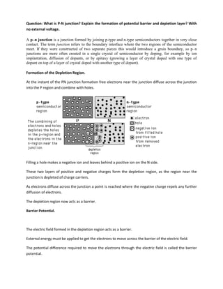
  • 1. Question: What is P-N junction? Explain the formation of potential barrier and depletion layer? With no external voltage. A p–n junction is a junction formed by joining p-type and n-type semiconductors together in very close contact. The term junction refers to the boundary interface where the two regions of the semiconductor meet. If they were constructed of two separate pieces this would introduce a grain boundary, so p–n junctions are more often created in a single crystal of semiconductor by doping, for example by ion implantation, diffusion of dopants, or by epitaxy (growing a layer of crystal doped with one type of dopant on top of a layer of crystal doped with another type of dopant). Formation of the Depletion Region. At the instant of the PN junction formation free electrons near the junction diffuse across the junction into the P region and combine with holes. Filling a hole makes a negative ion and leaves behind a positive ion on the N side. These two layers of positive and negative charges form the depletion region, as the region near the junction is depleted of charge carriers. As electrons diffuse across the junction a point is reached where the negative charge repels any further diffusion of electrons. The depletion region now acts as a barrier. Barrier Potential. The electric field formed in the depletion region acts as a barrier. External energy must be applied to get the electrons to move across the barrier of the electric field. The potential difference required to move the electrons through the electric field is called the barrier potential.
  • 2. Barrier potential of a PN junction depends on the type of semiconductor material, amount of doping and temperature. This is approximately 0.7V for silicon and 0.3V for germanium. Question: Draw the energy level diagram of a PN junction and explain how a junction barrier is developed across an unbiased junction. Energy Diagrams of PN Junction: The valence band and conduction band in N-Type material are slightly lower than that of P-Type material. As diffusion occurs the depletion region forms and the energy level of the N region conduction band drops, causing alignment of the top of the N region conduction band and the bottom of the P region conduction band. At this point the energy bands are at equilibrium. There is an energy gradient across the depletion region that a N region electron must climb to get to the P region. Biasing the PN Junction. Forward Bias. An external D.C. voltage is applied to a PN junction to bias it. Forward bias allows current through a PN junction.
  • 3. Bias voltage imparts sufficient energy to the free electrons so they overcome the barrier potential and move into the P region. Conduction occurs with electron current in the N-Type material and hole current in the P-Type material. As more electrons and holes flow in the depletion region the number of positive and negative ions is reduced, causing the depletion region to narrow. The energy loss in overcoming the barrier potential results in a voltage drop across the PN junction equal to the barrier potential. ( 0.7V for Si, 0.3V for Ge.) When a PN junction is forward biased the N region conduction band is raised to a higher level that overlaps with the P region conduction band.
  • 4. Reverse Bias Reverse bias prevents current flow through a PN junction. P N Reverse bias potential attracts the majority carriers away from the PN junction widening the depletion region. The potential across the depletion region is equal to the bias voltage. Reverse current can flow through the PN junction due to minority carriers. When a PN junction is reverse biased the energy hill increases. Reverse Breakdown. If the reverse bias voltage is increased to the breakdown voltage, the reverse current will drastically increase. This is due to collisions of fast minority carriers with atoms, knocking out valence electrons. This process avalanches and results in a high reverse current damaging the PN structure.
  • 5. Question: Explain the majority & minority carriers produces in n-type & t-type materials. Majority and Minority Carriers: In the intrinsic state, the number of free electrons in Ge or Si is due only to those few electrons in the valence band that have acquired sufficient energy from thermal or light sources to break the covalent bond or to the few impurities that could not be re-moved. The vacancies left behind in the covalent bonding structure represent our very limited supply of holes. In an n-type material, the number of holes has not changed significantly from this intrinsic level. The net result, therefore, is that the number of electrons far outweighs the number of holes. For this reason In an n- type material (Fig. 1.13a) the electron is called the majority carrier and the hole the minority carrier. For the p-type material the number of holes far outweighs the number of electrons, as shown in Fig. 1.13b. Therefore: In a p-type material the hole is the majority carrier and the electron is the minority carrier. When the fifth electron of a donor atom leaves the parent atom, the atom remaining acquires a net positive charge: hence the positive sign in the donor-ion representation. For similar reasons, the negative sign appears in the acceptor ion. The n- and p-type materials represent the basic building blocks of semiconductor devices. We will find in the next section that the “joining “of a single n-type material with a p-type material will result in a semiconductor element of considerable importance in electronic systems. Question: What is forward biasing & reverse biasing? Explain the PN Junction forward bias & reverse bias. Forward biasing: Forward bias occurs when the P-type semiconductor material is connected to the positive terminal of a battery and the N-type semiconductor material is connected to the negative terminal, as shown below. This usually makes the p–n junction conduct. With a battery connected this way, the holes in the P-type region and the electrons in the N-type region are pushed towards the junction. This reduces the width of the depletion zone. The positive charge applied to the P-type material repels the holes, while the negative charge applied to the N-type material repels the electrons. As electrons and holes are pushed towards the junction, the distance between them decreases. This lowers the barrier in potential. With increasing forward-bias voltage, the depletion zone eventually becomes thin enough that the zone's electric field can't counteract charge carrier motion across the p–n junction, consequently reducing electrical resistance. The electrons which cross the p–n junction into the P-type material (or holes which cross into the N-type material) will diffuse in the near-neutral region. Therefore,
  • 6. the amount of minority diffusion in the near-neutral zones determines the amount of current that may flow through the diode. Only majority carriers (electrons in N-type material or holes in P-type) can flow through a semiconductor for a macroscopic length. With this in mind, consider the flow of electrons across the junction. The forward bias causes a force on the electrons pushing them from the N side toward the P side. With forward bias, the depletion region is narrow enough that electrons can cross the junction and inject into the P-type material. However, they do not continue to flow through the P-type material indefinitely, because it is energetically favorable for them to recombine with holes. The average length an electron travels through the P-type material before recombining is called the diffusion length, and it is typically on the order of microns. Although the electrons penetrate only a short distance into the P-type material, the electric current continues uninterrupted, because holes (the majority carriers) begin to flow in the opposite direction. The total current (the sum of the electron and hole currents) is constant in space, because any variation would cause charge buildup over time (this is Kirchhoff's current law). The flow of holes from the P-type region into the N-type region is exactly analogous to the flow of electrons from N to P (electrons and holes swap roles and the signs of all currents and voltages are reversed). Therefore, the macroscopic picture of the current flow through the diode involves electrons flowing through the N-type region toward the junction, holes flowing through the P-type region in the opposite direction toward the junction, and the two species of carriers constantly recombining in the vicinity of the junction. The electrons and holes travel in opposite directions, but they also have opposite charges, so the overall current is in the same direction on both sides of the diode, as required. Reverse Bias: Reverse biased usually refers to how a diode is used in a circuit. If a diode is reverse biased, the voltage at the cathode is higher than that at the anode. Therefore, no current will flow until the diode breaks down. Connecting the P-type region to the negative terminal of the battery and the N-type region to the positive terminal, corresponds to reverse bias. The connections are illustrated in the following diagram: Because the p-type material is now connected to the negative terminal of the power supply, the 'holes' in the P-type material are pulled away from the junction, causing the width of the depletion zone to increase. Similarly, because the N-type region is connected to the positive terminal, the electrons will also be pulled away from the junction. Therefore the depletion region widens, and does so increasingly with increasing reverse-bias voltage. This increases the voltage barrier causing a high resistance to the flow of charge carriers thus allowing minimal electric current to cross the p–n junction. The strength of the depletion zone electric field increases as the reverse-bias voltage increases. Once the electric field intensity increases beyond a critical level, the p–n junction depletion zone breaks-down and current begins to flow, usually by either the Zener or avalanche breakdown processes. Both of these breakdown processes are non-destructive and are reversible, so long as
  • 7. the amount of current flowing does not reach levels that cause the semiconductor material to overheat and cause thermal damage. This effect is used to one's advantage in zener diode regulator circuits. Zener diodes have a certain - low - breakdown voltage. A standard value for breakdown voltage is for instance 5.6V. This means that the voltage at the cathode can never be more than 5.6V higher than the voltage at the anode, because the diode will break down - and therefore conduct - if the voltage gets any higher. This effectively regulates the voltage over the diode. Another application where reverse biased diodes are used is in Varicap diodes. The width of the depletion zone of any diode changes with voltage applied. This varies the capacitance of the diode. For more information, refer to the Varicap article. Question: What is break down? Explain zener break down and avalence break down? A Zener diode is a type of diode that permits current not only in the forward direction like a normal diode, but also in the reverse direction if the voltage is larger than the breakdown voltage known as "Zener knee voltage" or "Zener voltage". The device was named after Clarence Zener, who discovered this electrical property. A conventional solid-state diode will not allow significant current if it is reverse-biased below its reverse breakdown voltage. When the reverse bias breakdown voltage is exceeded, a conventional diode is subject to high current due to avalanche breakdown. Unless this current is limited by external circuitry, the diode will be permanently damaged. In case of large forward bias (current in the direction of the arrow), the diode exhibits a voltage drop due to its junction built-in voltage and internal resistance. The amount of the voltage drop depends on the semiconductor material and the doping concentrations. A Zener diode exhibits almost the same properties, except the device is specially designed so as to have a greatly reduced breakdown voltage, the so-called Zener voltage. By contrast with he conventional device, a reverse-biased Zener diode will exhibit a controlled breakdown and allow the current to keep the voltage across the Zener diode at the Zener voltage. For example, a diode with a Zener breakdown voltage of 3.2 V will exhibit a voltage drop of 3.2 V if reverse bias voltage applied across it is more than its Zener voltage. The Zener diode is therefore ideal for applications such as the generation of a reference voltage (e.g. for an amplifier stage), or as a voltage stabilizer for low-current applications.
  • 8. The Zener diode's operation depends on the heavy doping of its p-n junction allowing electrons to tunnel from the valence band of the p-type material to the conduction band of the n-type material. In the atomic scale, this tunneling corresponds to the transport of valence band electrons into the empty conduction band states; as a result of the reduced barrier between these bands and high electric fields that are induced due to the relatively high levels of dopings on both sides.The breakdown voltage can be controlled quite accurately in the doping process. While tolerances within 0.05% are available, the most widely used tolerances are 5% and 10%. Breakdown voltage for commonly available zener diodes can vary widely from 1.2 volts to 200 volts. Another mechanism that produces a similar effect is the avalanche effect as in the avalanche diode. The two types of diode are in fact constructed the same way and both effects are present in diodes of this type. In silicon diodes up to about 5.6 volts, the Zener effect is the predominant effect and shows a marked negative temperature coefficient. Above 5.6 volts, the avalanche effect becomes predominant and exhibits a positive temperature coefficient. In a 5.6 V diode, the two effects occur together and their temperature coefficients neatly cancel each other out, thus the 5.6 V diode is the component of choice in temperature-critical applications. Modern manufacturing techniques have produced devices with voltages lower than 5.6 V with negligible temperature coefficients, but as higher voltage devices are encountered, the temperature coefficient rises dramatically. A 75 V diode has 10 times the coefficient of a 12 V diode. All such diodes, regardless of breakdown voltage, are usually marketed under the umbrella term of "Zener diode". Avalanche breakdown: avalanche breakdown is a phenomenon that can occur in both insulating and semiconducting materials. It is a form of electric current multiplication that can allow very large currents to flow within materials which are otherwise good insulators. It is a type of electron avalanche. Explanation: Materials conduct electricity if they contain mobile charge carriers. There are two types of charge carrier in a semiconductor: free electrons and electron holes. A fixed electron in a reverse-biased diode may break free due to its thermal energy, creating an electron-hole pair. If there is a voltage gradient in the semiconductor, the electron will move towards the positive voltage while the hole will "move" towards the negative voltage. Most of the time, the electron and hole will just move to opposite ends of the crystal and stop. Under the right circumstances, however, (ie. when the voltage is high enough) the free electron may move fast enough to knock other electrons free, creating more free-electron-hole pairs (ie. more charge carriers), increasing the current. Fast-"moving" holes may also result in more electron-hole pairs being formed. In a fraction of a nanosecond, the whole crystal begins to conduct quite nicely. Avalanche breakdown usually destroys regular diodes, but avalanche diodes are designed to break down this way at low voltages and can survive the reverse current. The voltage at which the breakdown occurs is called the breakdown voltage. Once avalanche breakdown has occurred, the material will continue to conduct if the voltage across it drops below the breakdown voltage. This is different from a Zener diode because a Zener diode will stop conducting once the reverse voltage drops below the breakdown voltage.
  • 9. Question: What is knee voltage? The point or area on a graph of diode current versus voltage where the forward current suddenly increases. It is approximately equal to the barrier potential of the diode. Question: Explain V-I Characteristics of P-N junction. Forward biasing: A p-n junction is said to be forward biased, if the positive terminal of the external battery B is connected to p-side and the negative terminal to the n-side of the p-n junction. Here the forward bias opposes the potential barrier VB and so the depletion layer becomes thin. The majority charge carriers in the P type and N types are repelled by their respective terminals due to battery B and hence cross the junction. On crossing the junction, recombination process takes place. For every electron hole combination, a covalent bond near the +ve terminal of the battery B is broken and this liberates an electron which enters the +ve terminal of B through connecting wires. This in turn creates more holes in P-region. At the other end, the electrons from -ve terminal of B enter n-region to replace electron lost due to recombination process. Thus a large current will flow to migration of majority carriers across the p-n junction which is called forward current. Reverse biasing: A p-n junction is said to be reverse biased if the positive terminal of the battery B is connected to N-side and the negative terminal to p-side of the p-n junction. The majority carriers are pulled away from the junction and the depletion region becomes thick. The resistance becomes high when reverse biased and so there is no conduction across the junction due to majority carriers. The minority carriers however cross the junction and they constitute a current that flows in the opposite direction. This is the reverse current. The V-I characteristics of a p-n junction diode
  • 10. Question: What are LED? How do they works? Explain Briefly, mention some of it’s application. A light-emitting diode (LED) is a semiconductor light source. LEDs are used as indicator lamps in many devices, and are increasingly used for lighting. Introduced as a practical electronic component in 1962,[2] early LEDs emitted low-intensity red light, but modern versions are available across the visible, ultraviolet and infrared wavelengths, with very high brightness. The LED is based on the semiconductor diode. When a diode is forward biased (switched on), electrons are able to recombine with holes within the device, releasing energy in the form of photons. This effect is called electroluminescence and the color of the light (corresponding to the energy of the photon) is determined by the energy gap of the semiconductor. An LED is usually small in area (less than 1 mm2), and integrated optical components are used to shape its radiation pattern and assist in reflection.[3] LEDs present many advantages over incandescent light sources including lower energy consumption, longer lifetime, improved robustness, smaller size, faster switching, and greater durability and reliability. However, they are relatively expensive and require more precise current and heat management than traditional light sources. Current LED products for general lighting are more expensive to buy than fluorescent lamp sources of comparable output. They also enjoy use in applications as diverse as replacements for traditional light sources in automotive lighting (particularly indicators) and in traffic signals. The compact size of LEDs has allowed new text and video displays and sensors to be developed, while their high switching rates are useful in advanced communications technology. Application of LEDs fall into three major categories:  Visual signal application where the light goes more or less directly from the LED to the human eye, to convey a message or meaning.  Illumination where LED light is reflected from object to give visual response of these objects.  Generate light for measuring and interacting with processes that do not involve the human visual system. Question: How an ideal diode acts as a switch? The IDEAL DIODE serves as an electrical one-way valve. It conducts current much more readily in one direction, called the FORWARD (BIAS) DIRECTION, than it does in the other direction called the REVERSE (BIAS) DIRECTION. IDEAL DIODE acts like a SWITCH that closes to allow current flow in the forward direction but opens to prevent current flow in the reverse direction.
  • 11. Question: What is rectifier and rectification? Rectifier: Rectifier is an electrical device which can change an a.c current to d.c current. Rectification: The process of changes ac to d.c is called rectification. Question : What is half wave rectifier? Explain the use of a PN junction diode as a half wave rectifier? Find out the efficiency & ripple factor of a half wave rectifier? In half wave rectification, either the positive or negative half of the AC wave is passed, while the other half is blocked. Because only one half of the input waveform reaches the output, it is very inefficient if used for power transfer. Half-wave rectification can be achieved with a single diode in a one-phase supply, or with three diodes in a three-phase supply. • Average value of the output voltage, Vdc • Average value of the output current, Idc • Output dc power, Pdc – Pdc = VdcIdc • rms value of the output voltage, Vrms • Output ac power, Pac – Pac = VrmsIrms • Efficiency, η – η = Pdc/Pac • Effective (rms) value of the ac component of the output voltage, Vac – Vac = Vrms2 – Vdc2 • Form factor, FF – FF = Vrms/Vdc • Ripple factor, RF
  • 12. RF = Vac/Vdc • Alternate form for ripple factor • Transformer utilization factor, TUF – TUF = Pdc/VsIs – Vs, Is are rms voltage and current of the transformer secondary Determine the Average Voltage, Vdc
  • 13. .