Semiconductor
•Als PPTX, PDF herunterladen•
6 gefällt mir•5,531 views

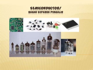
1) Semiconductors exhibit characteristics between conductors and insulators. Diodes and transistors are early components made from semiconductors. 2) There are two types of semiconductors - intrinsic and extrinsic. Intrinsic semiconductors do not contain any foreign atoms while extrinsic are created by diffusing or implanting impurities into intrinsic semiconductors. 3) Extrinsic semiconductors can be n-type or p-type depending on the impurity used - n-type uses elements like phosphorus that add free electrons, while p-type uses elements like boron that create holes. The combination of n-type and p-type materials creates the PN

Empfohlen
Weitere ähnliche Inhalte
Was ist angesagt?
Was ist angesagt? (20)
Andere mochten auch
Andere mochten auch (20)
Ähnlich wie Semiconductor
Ähnlich wie Semiconductor (20)
Kürzlich hochgeladen
Kürzlich hochgeladen (20)
Semiconductor
- 2. INTRODUCTION • Material which exhibit the characteristics between conductor and an insulator. • Diodes & transistor are the earliest component built from conductor.
- 3. TYPES OF SEMICONDUCTORS Semiconduktor Extrinsic P- type material N-type material Intrinsic
- 4. INTRINSIC intrinsik ialah separuh pengalir tulin dan tidak mengandungi unsur asing sedikitpyuun di dalamnya
- 5. EXTRINSIC Created when an impure atom is diffused or implanted into an intrinsic semiconductor. The process of diffusion or implantation impurities an the atom is known as doping. The purpose of doping is to increase the number of electron/holes to improve
- 6. N-TYPE MATERIAL Doped with pentavalent elements like phosphorus, arsenic, and antimony. Semikonduktor tulen diserapkan dengan bendasing pentavalen (contoh:Arsenik yang mempunyai 5 elektron valensi).. 4 daripada 5 elektron valensi atom Arsenik akan membentuk ikatan kovalen dengan atom--atom Silikon.. Satu elektron Arsenik Iagi tidak mempunyai pasangan.. Elektron ini akan terlepas dari orbitnya dan menjadi elektron bebas iaitu pembawa arus negatif.. Maka terhasillah semikonduktor jenis N..
- 7. P-TYPE MATERIAL • Semikonduktor tulen diserapkan dengan bendasing trivalen (contoh Indium) yang mempunyai 3 elektron valensi • Ketiga--tiga elektron valensi dari atom Indium akan membentuk ikatari kovalen dengan elektron valensi atom--atom silikon yang betlampiran.. • Satu Iagi elektron valensi atom siIikon tidak dapat membentuk ikatan kovalen.. • Kekosongan ini menghasilkan hol iaitu pembawa arus
- 8. CLASSIFICATION OF MATERIALS Atomic structure consists of three basic element: o Proton o Neutron o Electron Proton and neutron make up the nucleus. Electron spin in the orbit around the nucleus. Electrons are negatively charged and protons are positively charged. Atom is neutral when the value of proton and electron is equal. Neutron and proton has the same mass. The number of neutron in a nucleus determines the weight of an atom.
- 9. BOHRᶦS THEORY According to Bohr's theory, electron orbit around the nucleus at a specific energy level. The orbit or shell that used by the electrons to orbit around the nucleus is labelled K,L,M and N. The number of electron in each orbit is given by the formula 2n², with “n” representing the orbit number of shell position from the nucleus (that is n=1, 2, 3, ) Shell 1 = K Shell 2 = L Shell 3 =M Valence electron have the highest energy level. The number of valence electron is the different between the total electron in an atom and the total electron in orbit K, L, and M. The number of valence electron determines the classification of the element. The classification are classified into three type based on its ability to conduct current. ( conductor, insulator and semiconductor) conductor insulator semiconductor • an element that allows electrical current or free electron to flow through it easily. • only 1 or 2 electron are available in the valence orbit. •Very low number of valence electron, there Material that does not allow electric current to flow through it. Non-metallic element and has 5,6 or 7 valence electron. An atom has 8 valence electron and considered stable . is an element that has the characteristics between a conductor and insulator. has 4 valence electron. Resistance is not low as the resistance of a conductor and not as high as the resistance of an
- 10. BAND DIAGRAM Electron in orbit contain kinetic and electric potential energy. Orbit of atom are referred to as energy levels. Random movement of electron in orbit is influenced by the combination of the electric field of atom and other nearby
- 12. We will resolve the discussion of solids into three types, where bands are concerned:
- 15. INSULATOR insulators the electrons in the valence band are separated by a large gap from the conduction band, where there is no conductivity over a wide range of temperatures.
- 16. SEMICONDUCTOR semiconductors there is a small enough gap between the valence and conduction bands that thermal or other excitations can bridge the gap. With such a small gap, the presence of a small percentage of a doping material can increase conductivity dramatically. where there is no conductivity at
- 17. CONDUCTOR conductors like metals the valence band overlaps the conduction band, where the electrons in the highest energy levels are free to move along delocalized energy levels. Conductivity decreases as the temperature is raised.
- 18. CURRENT FLOW IN SEMICONDUCTOR N-type Materials P-type Materials • Occur simultaneously in two ways: i. Flow of free electron in the conduction band which is the majority current carrier ii.Flow of holes in valence band which is the minority •Occur simultaneously in two ways: i. Flow of holes in the valence band which is the majority current carrier, ii.Flow of free electron in the conduction band which is the
- 19. CURRENT FLOW IN N-TYPE MATERIALS
- 20. N-Types extrinsic semiconductor connected to a voltage source. Electrons move to positive terminal of the voltage source. Holes left behind because of the movement of the electron in the valence band seem to move to the negative terminal of the voltage source. In N-types material, most of current is due to electron because they are majority carrier. While holes are the minority carrier in N- types materials, thus the current due to holes is minimal. When the temperature of the semiconductor is
- 21. CURRENT FLOW IN P-TYPE MATERIALS
- 22. Holes repelled by the positive terminal of the voltage source will move towards the negative terminal of the voltage source. Free electron will move to the positive terminal of the voltage source. Current in N-type materials is greater than the current in the P- type materials because the electron movement in the conduction band is much easier compared to holes
- 23. THE MOVEMENT OF HOLES IN P-TYPE MATERIALS
- 24. PN JUNCTION i. .
- 25. i. When the two materials P-types and N-Types are combined they formed a PN junction. ii. The different structure of P-types and N-types materials allows the creation of devices such as diodes, unijunction transistor, bipolar junction transistor and field effect
- 26. END