
Empfohlen
Weitere ähnliche Inhalte
Was ist angesagt?
Was ist angesagt? (18)
Ähnlich wie CC2430 SoC for 2.4 GHz Wireless Applications
Ähnlich wie CC2430 SoC for 2.4 GHz Wireless Applications (20)
Kürzlich hochgeladen
Kürzlich hochgeladen (20)
CC2430 SoC for 2.4 GHz Wireless Applications
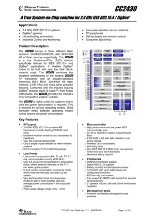
- 1. CC2430 A True System-on-Chip solution for 2.4 GHz IEEE 802.15.4 / ZigBee® Applications • 2.4 GHz IEEE 802.15.4 systems • Low power wireless sensor networks • ZigBee® systems • PC peripherals • Home/building automation • Set-top boxes and remote controls • Industrial Control and Monitoring • Consumer Electronics Product Description The CC2430 comes in three different flash versions: CC2430F32/64/128, with 32/64/128 KB of flash memory respectively. The CC2430 is a true System-on-Chip (SoC) solution specifically tailored for IEEE 802.15.4 and ZigBee® applications. It enables ZigBee® nodes to be built with very low total bill-of- material costs. The CC2430 combines the excellent performance of the leading CC2420 RF transceiver with an industry-standard enhanced 8051 MCU, 32/64/128 KB flash memory, 8 KB RAM and many other powerful features. Combined with the industry leading ZigBee® protocol stack (Z-Stack™) from Texas Instruments, the CC2430 provides the market’s most competitive ZigBee® solution. The CC2430 is highly suited for systems where ultra low power consumption is required. This is ensured by various operating modes. Short transition times between operating modes further ensure low power consumption. Key Features • RF/Layout • Microcontroller o 2.4 GHz IEEE 802.15.4 compliant RF o High performance and low power 8051 transceiver (industry leading CC2420 radio microcontroller core core) o 32, 64 or 128 KB in-system programmable o Excellent receiver sensitivity and robustness to flash interferers o 8 KB RAM, 4 KB with data retention in all o Very few external components power modes o Only a single crystal needed for mesh network o Powerful DMA functionality systems o Watchdog timer o RoHS compliant 7x7mm QLP48 package o One IEEE 802.15.4 MAC timer, one general 16-bit timer and two 8-bit timers • Low Power o Hardware debug support o Low current consumption (RX: 27 mA, TX: 27 mA, microcontroller running at 32 MHz) • Peripherals o Only 0.5 µA current consumption in powerdown o CSMA/CA hardware support. mode, where external interrupts or the RTC o Digital RSSI / LQI support can wake up the system o Battery monitor and temperature sensor o 0.3 µA current consumption in stand-by mode, o 12-bit ADC with up to eight inputs and where external interrupts can wake up the configurable resolution system o AES security coprocessor o Very fast transition times from low-power o Two powerful USARTs with support for several modes to active mode enables ultra low serial protocols average power consumption in low dutycycle o 21 general I/O pins, two with 20mA sink/source systems capability o Wide supply voltage range (2.0V - 3.6V) • Development tools o Powerful and flexible development tools available CC2430 Data Sheet (rev. 2.1) SWRS036F Page 1 of 211
- 2. CC2430 Table Of Contents 1 ABBREVIATIONS................................................................................................................................ 5 2 REFERENCES....................................................................................................................................... 7 3 REGISTER CONVENTIONS .............................................................................................................. 8 4 FEATURES EMPHASIZED ................................................................................................................ 9 4.1 HIGH-PERFORMANCE AND LOW-POWER 8051-COMPATIBLE MICROCONTROLLER ............................... 9 4.2 UP TO 128 KB NON-VOLATILE PROGRAM MEMORY AND 2 X 4 KB DATA MEMORY ............................ 9 4.3 HARDWARE AES ENCRYPTION/DECRYPTION ....................................................................................... 9 4.4 PERIPHERAL FEATURES ......................................................................................................................... 9 4.5 LOW POWER.......................................................................................................................................... 9 4.6 IEEE 802.15.4 MAC HARDWARE SUPPORT ........................................................................................... 9 4.7 INTEGRATED 2.4GHZ DSSS DIGITAL RADIO ........................................................................................ 9 5 ABSOLUTE MAXIMUM RATINGS ................................................................................................ 10 6 OPERATING CONDITIONS............................................................................................................. 10 7 ELECTRICAL SPECIFICATIONS .................................................................................................. 11 7.1 GENERAL CHARACTERISTICS .............................................................................................................. 12 7.2 RF RECEIVE SECTION ......................................................................................................................... 13 7.3 RF TRANSMIT SECTION ....................................................................................................................... 13 7.4 32 MHZ CRYSTAL OSCILLATOR .......................................................................................................... 14 7.5 32.768 KHZ CRYSTAL OSCILLATOR .................................................................................................... 14 7.6 32 KHZ RC OSCILLATOR..................................................................................................................... 15 7.7 16 MHZ RC OSCILLATOR ................................................................................................................... 15 7.8 FREQUENCY SYNTHESIZER CHARACTERISTICS ................................................................................... 16 7.9 ANALOG TEMPERATURE SENSOR ........................................................................................................ 16 7.10 ADC ................................................................................................................................................... 16 7.11 CONTROL AC CHARACTERISTICS........................................................................................................ 18 7.12 SPI AC CHARACTERISTICS ................................................................................................................. 19 7.13 DEBUG INTERFACE AC CHARACTERISTICS ......................................................................................... 20 7.14 PORT OUTPUTS AC CHARACTERISTICS ............................................................................................... 21 7.15 TIMER INPUTS AC CHARACTERISTICS................................................................................................. 21 7.16 DC CHARACTERISTICS ........................................................................................................................ 21 8 PIN AND I/O PORT CONFIGURATION ........................................................................................ 22 9 CIRCUIT DESCRIPTION ................................................................................................................. 24 9.1 CPU AND PERIPHERALS ...................................................................................................................... 25 9.2 RADIO ................................................................................................................................................. 26 10 APPLICATION CIRCUIT ................................................................................................................. 27 10.1 INPUT / OUTPUT MATCHING ................................................................................................................. 27 10.2 BIAS RESISTORS .................................................................................................................................. 27 10.3 CRYSTAL ............................................................................................................................................. 27 10.4 VOLTAGE REGULATORS ...................................................................................................................... 27 10.5 DEBUG INTERFACE .............................................................................................................................. 27 10.6 POWER SUPPLY DECOUPLING AND FILTERING...................................................................................... 28 11 8051 CPU .............................................................................................................................................. 30 11.1 8051 CPU INTRODUCTION .................................................................................................................. 30 11.2 MEMORY ............................................................................................................................................. 30 11.3 CPU REGISTERS .................................................................................................................................. 42 11.4 INSTRUCTION SET SUMMARY .............................................................................................................. 44 11.5 INTERRUPTS ........................................................................................................................................ 49 12 DEBUG INTERFACE......................................................................................................................... 60 12.1 DEBUG MODE ..................................................................................................................................... 60 12.2 DEBUG COMMUNICATION ................................................................................................................... 60 12.3 DEBUG COMMANDS ............................................................................................................................ 60 12.4 DEBUG LOCK BIT ................................................................................................................................ 60 12.5 DEBUG INTERFACE AND POWER MODES ............................................................................................. 64 13 PERIPHERALS ................................................................................................................................... 65 CC2430 Data Sheet (rev. 2.1) SWRS036F Page 2 of 211
- 3. CC2430 13.1 POWER MANAGEMENT AND CLOCKS ................................................................................................... 65 13.2 RESET ................................................................................................................................................. 71 13.3 FLASH CONTROLLER ........................................................................................................................... 71 13.4 I/O PORTS ............................................................................................................................................ 77 13.5 DMA CONTROLLER ............................................................................................................................ 88 13.6 16-BIT TIMER, TIMER1 ........................................................................................................................ 99 13.7 MAC TIMER (TIMER2)...................................................................................................................... 110 13.8 8-BIT TIMERS, TIMER 3 AND TIMER 4 ................................................................................................ 117 13.9 SLEEP TIMER ..................................................................................................................................... 126 13.10 ADC ................................................................................................................................................. 128 13.11 RANDOM NUMBER GENERATOR ....................................................................................................... 134 13.12 AES COPROCESSOR .......................................................................................................................... 136 13.13 WATCHDOG TIMER ........................................................................................................................... 141 13.14 USART............................................................................................................................................. 143 14 RADIO ................................................................................................................................................ 153 14.1 IEEE 802.15.4 MODULATION FORMAT ............................................................................................. 154 14.2 COMMAND STROBES ......................................................................................................................... 155 14.3 RF REGISTERS................................................................................................................................... 155 14.4 INTERRUPTS ...................................................................................................................................... 155 14.5 FIFO ACCESS .................................................................................................................................... 157 14.6 DMA ................................................................................................................................................ 157 14.7 RECEIVE MODE.................................................................................................................................. 158 14.8 RXFIFO OVERFLOW ......................................................................................................................... 158 14.9 TRANSMIT MODE ............................................................................................................................... 159 14.10 GENERAL CONTROL AND STATUS ...................................................................................................... 160 14.11 DEMODULATOR, SYMBOL SYNCHRONIZER AND DATA DECISION ..................................................... 160 14.12 FRAME FORMAT ................................................................................................................................ 161 14.13 SYNCHRONIZATION HEADER ............................................................................................................. 161 14.14 LENGTH FIELD ................................................................................................................................... 162 14.15 MAC PROTOCOL DATA UNIT ............................................................................................................. 162 14.16 FRAME CHECK SEQUENCE ................................................................................................................. 162 14.17 RF DATA BUFFERING ........................................................................................................................ 163 14.18 ADDRESS RECOGNITION .................................................................................................................... 164 14.19 ACKNOWLEDGE FRAMES .................................................................................................................. 165 14.20 RADIO CONTROL STATE MACHINE ..................................................................................................... 166 14.21 MAC SECURITY OPERATIONS (ENCRYPTION AND AUTHENTICATION).............................................. 168 14.22 LINEAR IF AND AGC SETTINGS ........................................................................................................ 168 14.23 RSSI / ENERGY DETECTION .............................................................................................................. 168 14.24 LINK QUALITY INDICATION .............................................................................................................. 168 14.25 CLEAR CHANNEL ASSESSMENT......................................................................................................... 169 14.26 FREQUENCY AND CHANNEL PROGRAMMING ..................................................................................... 169 14.27 VCO AND PLL SELF-CALIBRATION .................................................................................................. 169 14.28 OUTPUT POWER PROGRAMMING ....................................................................................................... 170 14.29 INPUT / OUTPUT MATCHING .............................................................................................................. 170 14.30 TRANSMITTER TEST MODES ............................................................................................................. 171 14.31 SYSTEM CONSIDERATIONS AND GUIDELINES .................................................................................... 173 14.32 PCB LAYOUT RECOMMENDATION .................................................................................................... 175 14.33 ANTENNA CONSIDERATIONS ............................................................................................................. 175 14.34 CSMA/CA STROBE PROCESSOR ....................................................................................................... 176 14.35 RADIO REGISTERS ............................................................................................................................. 183 15 VOLTAGE REGULATORS............................................................................................................. 202 15.1 VOLTAGE REGULATORS POWER-ON.................................................................................................. 202 16 EVALUATION SOFTWARE........................................................................................................... 202 17 REGISTER OVERVIEW ................................................................................................................. 203 18 PACKAGE DESCRIPTION (QLP 48) ............................................................................................ 206 18.1 RECOMMENDED PCB LAYOUT FOR PACKAGE (QLP 48).................................................................... 207 18.2 PACKAGE THERMAL PROPERTIES....................................................................................................... 207 18.3 SOLDERING INFORMATION ................................................................................................................ 207 18.4 TRAY SPECIFICATION ........................................................................................................................ 207 CC2430 Data Sheet (rev. 2.1) SWRS036F Page 3 of 211
- 4. CC2430 18.5 CARRIER TAPE AND REEL SPECIFICATION .......................................................................................... 207 19 ORDERING INFORMATION......................................................................................................... 209 20 GENERAL INFORMATION ........................................................................................................... 210 20.1 DOCUMENT HISTORY ........................................................................................................................ 210 21 ADDRESS INFORMATION ............................................................................................................ 210 22 TI WORLDWIDE TECHNICAL SUPPORT ................................................................................. 210 CC2430 Data Sheet (rev. 2.1) SWRS036F Page 4 of 211
- 5. CC2430 1 Abbreviations ADC Analog to Digital Converter I/O Input / Output AES Advanced Encryption Standard I/Q In-phase / Quadrature-phase AGC Automatic Gain Control IEEE Institute of Electrical and Electronics Engineers ARIB Association of Radio Industries and Businesses IF Intermediate Frequency BCD Binary Coded Decimal INL Integral Nonlinearity BER Bit Error Rate IOC I/O Controller BOD Brown Out Detector IRQ Interrupt Request BOM Bill of Materials ISM Industrial, Scientific and Medical CBC Cipher Block Chaining ITU-T International Telecommunication Union – Telecommunication Standardization CBC-MAC Cipher Block Chaining Message Sector Authentication Code IV Initialization Vector CCA Clear Channel Assessment JEDEC Joint Electron Device Engineering CCM Counter mode + CBC-MAC Council CFB Cipher Feedback KB 1024 bytes CFR Code of Federal Regulations kbps kilo bits per second CMOS Complementary Metal Oxide LC Inductor-capacitor Semiconductor LFSR Linear Feedback Shift Register CMRR Common Mode Ratio Recjection LNA Low-Noise Amplifier CPU Central Processing Unit LO Local Oscillator CRC Cyclic Redundancy Check LQI Link Quality Indication CSMA-CA Carrier Sense Multiple Access with Collision Avoidance LSB Least Significant Bit / Byte CSP CSMA/CA Strobe Processor LSB Least Significant Byte CTR Counter mode (encryption) MAC Medium Access Control CW Continuous Wave MAC Message Authentication Code DAC Digital to Analog Converter MCU Microcontroller Unit DC Direct Current MFR MAC Footer DMA Direct Memory Access MHR MAC Header DNL Differential Nonlineraity MIC Message Integrity Code DSM Delta Sigma Modulator MISO Master In Slave Out DSSS Direct Sequence Spread Spectrum MOSI Master Out Slave In ECB Electronic Code Book (encryption) MPDU MAC Protocol Data Unit EM Evaluation Module MSB Most Significant Byte ENOB Effective Number of bits MSDU MAC Service Data Unit ESD Electro Static Discharge MUX Multiplexer ESR Equivalent Series Resistance NA Not Available ETSI European Telecommunications NC Not Connected Standards Institute OFB Output Feedback (encryption) EVM Error Vector Magnitude O-QPSK Offset - Quadrature Phase Shift Keying FCC Federal Communications Commission PA Power Amplifier FCF Frame Control Field PCB Printed Circuit Board FCS Frame Check Sequence PER Packet Error Rate FFCTRL FIFO and Frame Control PHR PHY Header FIFO First In First Out PHY Physical Layer HF High Frequency PLL Phase Locked Loop HSSD High Speed Serial Data CC2430 Data Sheet (rev. 2.1) SWRS036F Page 5 of 211
- 6. CC2430 PM{0-3} Power Mode 0-3 SPI Serial Peripheral Interface PMC Power Management Controller SRAM Static Random Access Memory POR Power On Reset ST Sleep Timer PSDU PHY Service Data Unit T/R Tape and reel PWM Pulse Width Modulator T/R Transmit / Receive QLP Quad Leadless Package TBD To Be Decided / To Be Defined RAM Random Access Memory THD Total Harmonic Distortion RBW Resolution Bandwidth TI Texas Instruments RC Resistor-Capacitor TX Transmit RCOSC RC Oscillator UART Universal Asynchronous Receiver/Transmitter RF Radio Frequency USART Universal Synchronous/Asynchronous RoHS Restriction on Hazardous Substances Receiver/Transmitter RSSI Receive Signal Strength Indicator VCO Voltage Controlled Oscillator RTC Real-Time Clock VGA Variable Gain Amplifier RX Receive WDT Watchdog Timer SCK Serial Clock XOSC Crystal Oscillator SFD Start of Frame Delimiter SFR Special Function Register SHR Synchronization Header SINAD Signal-to-noise and distortion ratio CC2430 Data Sheet (rev. 2.1) SWRS036F Page 6 of 211
- 7. CC2430 2 References [1] IEEE std. 802.15.4 - 2003: Wireless Medium Access Control (MAC) and Physical Layer (PHY) specifications for Low Rate Wireless Personal Area Networks (LR-WPANs) http://standards.ieee.org/getieee802/download/802.15.4-2003.pdf [2] NIST FIPS Pub 197: Advanced Encryption Standard (AES), Federal Information Processing Standards Publication 197, US Department of Commerce/N.I.S.T., November 26, 2001. Available from the NIST website. http://csrc.nist.gov/publications/fips/fips197/fips-197.pdf CC2430 Data Sheet (rev. 2.1) SWRS036F Page 7 of 211
- 8. CC2430 3 Register conventions Each SFR register is described in a separate REGISTER NAME (XDATA Address) table. The table heading is given in the In the register descriptions, each register bit is following format: shown with a symbol indicating the access REGISTER NAME (SFR Address) - Register mode of the register bit. The register values Description. are always given in binary notation unless prefixed by ‘0x’ which indicates hexadecimal Each RF register is described in a separate notation. table. The table heading is given in the following format: Table 1: Register bit conventions Symbol Access Mode R/W Read/write R Read only R0 Read as 0 R1 Read as 1 W Write only W0 Write as 0 W1 Write as 1 H0 Hardware clear H1 Hardware set CC2430 Data Sheet (rev. 2.1) SWRS036F Page 8 of 211
- 9. CC2430 4 Features Emphasized 4.1 High-Performance and Low-Power 4.5 Low Power 8051-Compatible Microcontroller • Four flexible power modes for reduced • Optimized 8051 core, which typically power consumption gives 8x the performance of a standard • System can wake up on external 8051 interrupt or real-time counter event • Dual data pointers • Low-power fully static CMOS design • In-circuit interactive debugging is • System clock source can be 16 MHz RC supported for the IAR Embedded oscillator or 32 MHz crystal oscillator. Workbench through a simple two-wire The 32 MHz oscillator is used when serial interface radio is active 4.2 Up to 128 KB Non-volatile Program • Optional clock source for ultra-low power Memory and 2 x 4 KB Data Memory operation can be either low-power RC oscillator or an optional 32.768 kHz • 32/64/128 KB of non-volatile flash crystal oscillator memory in-system programmable through a simple two-wire interface or by 4.6 IEEE 802.15.4 MAC hardware support the 8051 core • Automatic preamble generator • Worst-case flash memory endurance: 1000 write/erase cycles • Synchronization word insertion/detection • Programmable read and write lock of • CRC-16 computation and checking over portions of Flash memory for software the MAC payload security • Clear Channel Assessment • 4096 bytes of internal SRAM with data • Energy detection / digital RSSI retention in all power modes • Link Quality Indication • Additional 4096 bytes of internal SRAM • CSMA/CA Coprocessor with data retention in power modes 0 and 1 4.7 Integrated 2.4GHz DSSS Digital Radio 4.3 Hardware AES Encryption/Decryption • 2.4 GHz IEEE 802.15.4 compliant RF transceiver (based on industry leading • AES supported in hardware coprocessor CC2420 radio core). 4.4 Peripheral Features • Excellent receiver sensitivity and robustness to interferers • Powerful DMA Controller • 250 kbps data rate, 2 MChip/s chip rate • Power On Reset/Brown-Out Detection • Reference designs comply with • Eight channel ADC with configurable worldwide radio frequency regulations resolution covered by ETSI EN 300 328 and EN • Programmable watchdog timer 300 440 class 2 (Europe), FCC CFR47 Part 15 (US) and ARIB STD-T66 • Real time clock with 32.768 kHz crystal (Japan). Transmit on 2480MHz under oscillator FCC is supported by duty-cycling, or by • Four timers: one general 16-bit timer, reducing output power. two general 8-bit timers, one MAC timer • Two programmable USARTs for master/slave SPI or UART operation • 21 configurable general-purpose digital I/O-pins • True random number generator CC2430 Data Sheet (rev. 2.1) SWRS036F Page 9 of 211
- 10. CC2430 5 Absolute Maximum Ratings Under no circumstances must the absolute maximum ratings given in Table 2 be violated. Stress exceeding one or more of the limiting values may cause permanent damage to the device. Table 2: Absolute Maximum Ratings Parameter Min Max Units Condition Supply voltage –0.3 3.9 V All supply pins must have the same voltage Voltage on any digital pin –0.3 VDD+0.3, V max 3.9 Voltage on the 1.8V pins (pin no. –0.3 2.0 V 22, 25-40 and 42) Input RF level 10 dBm Storage temperature range –50 150 °C Device not programmed Reflow soldering temperature 260 °C According to IPC/JEDEC J-STD-020C On RF pads (RF_P, RF_N, AVDD_RF1, <500 V and AVDD_RF2), according to Human Body Model, JEDEC STD 22, method A114 ESD All other pads, according to Human Body 700 V Model, JEDEC STD 22, method A114 According to Charged Device Model, 200 V JEDEC STD 22, method C101 Caution! ESD sensitive device. Precaution should be used when handling the device in order to prevent permanent damage. 6 Operating Conditions The operating conditions for CC2430 are listed in Table 3 . Table 3: Operating Conditions Parameter Min Max Unit Condition Operating ambient temperature -40 85 °C range, TA Operating supply voltage 2.0 3.6 V The supply pins to the radio part must be driven by the 1.8 V on-chip regulator CC2430 Data Sheet (rev. 2.1) SWRS036F Page 10 of 211
- 11. CC2430 7 Electrical Specifications Measured on Texas Instruments CC2430 EM reference design with TA=25°C and VDD=3.0V unless stated otherwise. Table 4: Electrical Specifications Parameter Min Typ Max Unit Condition Current Consumption Digital regulator on. 16 MHz RCOSC running. No radio, MCU Active Mode, 16 MHz, crystals, or peripherals active. 4.3 mA low MCU activity Low MCU activity: no flash access (i.e. only cache hit), no RAM access. Digital regulator on. 16 MHz RCOSC running. No radio, MCU Active Mode, 16 MHz, crystals, or peripherals active. 5.1 mA medium MCU activity 1 Medium MCU activity: normal flash access , minor RAM access. Digital regulator on. 16 MHz RCOSC running. No radio, MCU Active Mode, 16 MHz, crystals, or peripherals active. 5.7 mA high MCU activity 1 High MCU activity: normal flash access , extensive RAM access and heavy CPU load. 32 MHz XOSC running. No radio or peripherals active. MCU Active Mode, 32 MHz, 9.5 mA Low MCU activity : no flash access (i.e. only cache hit), low MCU activity no RAM access 32 MHz XOSC running. No radio or peripherals active. MCU Active Mode, 32 MHz, 10.5 mA 1 Medium MCU activity: normal flash access , minor RAM medium MCU activity access. 32 MHz XOSC running. No radio or peripherals active. MCU Active Mode, 32 MHz, 12.3 mA 1 High MCU activity: normal flash access , extensive RAM high MCU activity access and heavy CPU load. MCU running at full speed (32MHz), 32MHz XOSC MCU Active and RX Mode 26.7 mA running, radio in RX mode, -50 dBm input power. No peripherals active. Low MCU activity. MCU running at full speed (32MHz), 32MHz XOSC MCU Active and TX Mode, 0dBm 26.9 mA running, radio in TX mode, 0dBm output power. No peripherals active. Low MCU activity. Digital regulator on, 16 MHz RCOSC and 32 MHz crystal Power mode 1 190 µA oscillator off. 32.768 kHz XOSC, POR and ST active. RAM retention. Digital regulator off, 16 MHz RCOSC and 32 MHz crystal Power mode 2 0.5 µA oscillator off. 32.768 kHz XOSC, POR and ST active. RAM retention. Power mode 3 0.3 µA No clocks. RAM retention. POR active. Peripheral Current Adds to the figures above if the peripheral unit is Consumption activated Timer 1 150 µA Timer running, 32MHz XOSC used. Timer 2 230 µA Timer running, 32MHz XOSC used. Timer 3 50 µA Timer running, 32MHz XOSC used. Timer 4 50 µA Timer running, 32MHz XOSC used. Sleep Timer 0.2 µA Including 32.753 kHz RCOSC. ADC 1.2 mA When converting. Flash write 3 mA Estimated value Flash erase 3 mA Estimated value 1 Normal Flash access means that the code used exceeds the cache storage (see last paragraph in section 11.2.3 Flash memory) so cache misses will happen frequently. CC2430 Data Sheet (rev. 2.1) SWRS036F Page 11 of 211
- 12. CC2430 7.1 General Characteristics Measured on Texas Instruments CC2430 EM reference design with TA=25°C and VDD=3.0V unless stated otherwise. Table 5: General Characteristics Parameter Min Typ Max Unit Condition/Note Wake-Up and Timing Digital regulator on, 16 MHz RCOSC and Power mode 1 power 4.1 µs 32 MHz crystal oscillator off. Start-up of mode 0 16 MHz RCOSC. Digital regulator off, 16 MHz RCOSC and Power mode 2 or 3 power 120 µs 32 MHz crystal oscillator off. Start-up of mode 0 regulator and 16 MHz RCOSC. Time from enabling radio part in power Active TX or RX mode 0, until TX or RX starts. Includes 32MHz XOSC initially OFF. 525 µs start-up of voltage regulator and crystal Voltage regulator initially OFF oscillator in parallel. Crystal ESR=16Ω. Time from enabling radio part in power Active TX or RX 320 µs mode 0, until TX or RX starts. Includes Voltage regulator initially OFF start-up of voltage regulator. Radio part already enabled. Active RX or TX 192 µs Time until RX or TX starts. RX/TX turnaround 192 µs Radio part RF Frequency Range 2400 2483.5 MHz Programmable in 1 MHz steps, 5 MHz between channels for compliance with [1] Radio bit rate 250 kbps As defined by [1] Radio chip rate 2.0 MChip/s As defined by [1] CC2430 Data Sheet (rev. 2.1) SWRS036F Page 12 of 211
- 13. CC2430 7.2 RF Receive Section Measured on Texas Instruments CC2430 EM reference design with TA=25°C and VDD=3.0V unless stated otherwise. Table 6: RF Receive Parameters Parameter Min Typ Max Unit Condition/Note Receiver sensitivity -92 dBm PER = 1%, as specified by [1] Measured in 50 Ω single endedly through a balun. [1] requires –85 dBm Saturation (maximum input 10 dBm PER = 1%, as specified by [1] level) Measured in 50 Ω single endedly through a balun. [1] requires –20 dBm Adjacent channel rejection Wanted signal -88dBm, adjacent modulated channel + 5 MHz channel spacing 41 dB at +5 MHz, PER = 1 %, as specified by [1]. [1] requires 0 dB Adjacent channel rejection Wanted signal -88dBm, adjacent modulated channel - 5 MHz channel spacing 30 dB at -5 MHz, PER = 1 %, as specified by [1]. [1] requires 0 dB Alternate channel rejection Wanted signal -88dBm, adjacent modulated channel + 10 MHz channel spacing 55 dB at +10 MHz, PER = 1 %, as specified by [1] [1] requires 30 dB Alternate channel rejection Wanted signal -88dBm, adjacent modulated channel - 10 MHz channel spacing 53 dB at -10 MHz, PER = 1 %, as specified by [1] [1] requires 30 dB Channel rejection Wanted signal @ -82 dBm. Undesired signal is an ≥ + 15 MHz 55 dB 802.15.4 modulated channel, stepped through all channels from 2405 to 2480 MHz. Signal level for ≤ - 15 MHz 53 dB PER = 1%. Values are estimated. Co-channel rejection Wanted signal @ -82 dBm. Undesired signal is -6 dB 802.15.4 modulated at the same frequency as the desired signal. Signal level for PER = 1%. Blocking / Desensitization + 5 MHz from band edge -42 dBm Wanted signal 3 dB above the sensitivity level, CW + 10 MHz from band edge -45 dBm jammer, PER = 1%. Measured according to EN 300 + 20 MHz from band edge -26 dBm 440 class 2. + 50 MHz from band edge -22 dBm - 5 MHz from band edge -31 dBm - 10 MHz from band edge -36 dBm - 20 MHz from band edge -24 dBm - 50 MHz from band edge -25 dBm Spurious emission 30 – 1000 MHz −64 dBm Conducted measurement in a 50 Ω single ended 1 – 12.75 GHz −75 dBm load. Complies with EN 300 328, EN 300 440 class 2, FCC CFR47, Part 15 and ARIB STD-T-66. Frequency error tolerance ±140 ppm Difference between centre frequency of the received RF signal and local oscillator frequency. [1] requires minimum 80 ppm Symbol rate error tolerance ±900 ppm Difference between incoming symbol rate and the internally generated symbol rate [1] requires minimum 80 ppm 7.3 RF Transmit Section Measured on Texas Instruments CC2430 EM reference design with TA=25°C, VDD=3.0V, and nominal output power unless stated otherwise. CC2430 Data Sheet (rev. 2.1) SWRS036F Page 13 of 211
- 14. CC2430 Table 7: RF Transmit Parameters Parameter Min Typ Max Unit Condition/Note Nominal output 0 dBm Delivered to a single ended 50 Ω load through a balun and power output power control set to 0x5F (TXCTRLL). [1] requires minimum –3 dBm Programmable 26 dB The output power is programmable in 16 steps from typically output power range -25.2 to 0.6 dBm (see Table 45). Harmonics nd 2 harmonic -50.7 dBm Measurement conducted with 100 kHz resolution bandwidth on rd 3 harmonic -55.8 dBm spectrum analyzer and output power control set to 0x5F th (TXCTRLL). Output Delivered to a single ended 50 Ω load 4 harmonic -54.2 dBm through a balun. th 5 harmonic -53.4 dBm Spurious emission Maximum output power. 30 - 1000 MHz -47 dBm Texas Instruments CC2430 EM reference design complies with EN 300 328, EN 300 440, FCC CFR47 Part 15 and ARIB STD- 1– 12.75 GHz -43 dBm T-66. 1.8 – 1.9 GHz -58 dBm Transmit on 2480MHz under FCC is supported by duty-cycling, 5.15 – 5.3 GHz -56 dBm or by reducing output power The peak conducted spurious emission is -47 dBm @ 192 MHz which is in an EN 300 440 restricted band limited to -54 dBm. All radiated spurious emissions are within the limits of ETSI/FCC/ARIB. Conducted spurious emission (CSE) can be reduced with a simple band pass filter connected between matching network and RF connector (1.8 pF in parallel with 1.6 nH reduces the CSE by 20 dB), this filter must be connected to good RF ground. Error Vector 11 % Measured as defined by [1] Magnitude (EVM) [1] requires max. 35 % Optimum load 60 Ω Differential impedance as seen from the RF-port (RF_P and impedance + j164 RF_N) towards the antenna2. 7.4 32 MHz Crystal Oscillator Measured on Texas Instruments CC2430 EM reference design with TA=25°C and VDD=3.0V unless stated otherwise. Table 8: 32 MHz Crystal Oscillator Parameters Parameter Min Typ Max Unit Condition/Note Crystal frequency 32 MHz Crystal frequency - 40 40 ppm Including aging and temperature dependency, as specified by [1] accuracy requirement ESR 6 16 60 Ω Simulated over operating conditions C0 1 1.9 7 pF Simulated over operating conditions CL 10 13 16 pF Simulated over operating conditions Start-up time 212 µs 7.5 32.768 kHz Crystal Oscillator Measured on Texas Instruments CC2430 EM reference design with TA=25°C and VDD=3.0V unless stated otherwise. 2 This is for 2440MHz CC2430 Data Sheet (rev. 2.1) SWRS036F Page 14 of 211
- 15. CC2430 Table 9: 32.768 kHz Crystal Oscillator Parameters Parameter Min Typ Max Unit Condition/Note Crystal frequency 32.768 kHz Crystal frequency –40 40 ppm Including aging and temperature dependency, as specified by [1] accuracy requirement ESR 40 130 kΩ Simulated over operating conditions C0 0.9 2.0 pF Simulated over operating conditions CL 12 16 pF Simulated over operating conditions Start-up time 400 ms Value is simulated. 7.6 32 kHz RC Oscillator Measured on Texas Instruments CC2430 EM reference design with TA=25°C and VDD=3.0V unless stated otherwise. Table 10: 32 kHz RC Oscillator parameters Parameter Min Typ Max Unit Condition/Note Calibrated frequency 32.753 kHz The calibrated 32 kHz RC Oscillator frequency is the 32 MHz XTAL frequency divided by 977 Frequency accuracy after ±0.2 % Value is estimated. calibration Temperature coefficient +0.4 % / °C Frequency drift when temperature changes after calibration. Value is estimated. Supply voltage coefficient +3 %/V Frequency drift when supply voltage changes after calibration. Value is estimated. Initial calibration time 1.7 ms When the 32 kHz RC Oscillator is enabled, calibration is continuously done in the background as long as the 32 MHz crystal oscillator is running and SLEEP.OSC32K_CALDIS bit is cleared. 7.7 16 MHz RC Oscillator Measured on Texas Instruments CC2430 EM reference design with TA=25°C and VDD=3.0V unless stated otherwise. Table 11: 16 MHz RC Oscillator parameters Parameter Min Typ Max Unit Condition/Note Frequency 16 MHz The calibrated 16 MHz RC Oscillator frequency is the 32 MHz XTAL frequency divided by 2 Uncalibrated frequency ±18 % accuracy Calibrated frequency ±0.6 ±1 % accuracy Start-up time 10 µs Temperature coefficient -325 ppm / °C Frequency drift when temperature changes after calibration Supply voltage coefficient 28 ppm / mV Frequency drift when supply voltage changes after calibration Initial calibration time 50 µs When the 16 MHz RC Oscillator is enabled it will be calibrated continuously when the 32MHz crystal oscillator is running. CC2430 Data Sheet (rev. 2.1) SWRS036F Page 15 of 211
- 16. CC2430 7.8 Frequency Synthesizer Characteristics Measured on Texas Instruments CC2430 EM reference design with TA=25°C and VDD=3.0V unless stated otherwise. Table 12: Frequency Synthesizer Parameters Parameter Min Typ Max Unit Condition/Note Phase noise Unmodulated carrier −116 dBc/Hz At ±1.5 MHz offset from carrier −117 dBc/Hz At ±3 MHz offset from carrier −118 dBc/Hz At ±5 MHz offset from carrier PLL lock time 192 µs The startup time until RX/TX turnaround. The crystal oscillator is running. 7.9 Analog Temperature Sensor Measured on Texas Instruments CC2430 EM reference design with TA=25°C and VDD=3.0V unless stated otherwise. Table 13: Analog Temperature Sensor Parameters Parameter Min Typ Max Unit Condition/Note Output voltage at –40°C 0.648 V Value is estimated Output voltage at 0°C 0.743 V Value is estimated Output voltage at +40°C 0.840 V Value is estimated Output voltage at +80°C 0.939 V Value is estimated Temperature coefficient 2.45 mV/°C Fitted from –20°C to +80°C on estimated values. Absolute error in calculated –8 °C From –20°C to +80°C when assuming best fit for temperature absolute accuracy on estimated values: 0.743V at 0°C and 2.45mV / °C. Error in calculated -2 0 2 °C From –20°C to +80°C when using 2.45mV / °C, temperature, calibrated after 1-point calibration at room temperature. Values are estimated. Indicated min/max with 1- point calibration is based on simulated values for typical process parameters Current consumption 280 µA increase when enabled 7.10 ADC Measured with TA=25°C and VDD=3.0V. Note that other data may result using Texas Instruments CC2430 EM reference design. Table 14: ADC Characteristics Parameter Min Typ Max Unit Condition/Note Input voltage 0 VDD V VDD is voltage on AVDD_SOC pin External reference voltage 0 VDD V VDD is voltage on AVDD_SOC pin External reference voltage 0 VDD V VDD is voltage on AVDD_SOC pin differential Input resistance, signal 197 kΩ Simulated using 4 MHz clock speed (see section 13.10.2.7) 3 Full-Scale Signal 2.97 V Peak-to-peak, defines 0dBFS 3 Measured with 300 Hz Sine input and VDD as reference. CC2430 Data Sheet (rev. 2.1) SWRS036F Page 16 of 211
- 17. CC2430 Parameter Min Typ Max Unit Condition/Note 3 ENOB 5.7 bits 7-bits setting. Single ended input 7.5 9-bits setting. 9.3 10-bits setting. 10.8 12-bits setting. 3 ENOB 6.5 bits 7-bits setting. Differential input 8.3 9-bits setting. 10.0 10-bits setting. 11.5 12-bits setting. Useful Power Bandwidth 0-20 kHz 7-bits setting, both single and differential 3 THD -Single ended input -75.2 dB 12-bits setting, -6dBFS -Differential input -86.6 dB 12-bits setting, -6dBFS 3 Signal To Non-Harmonic Ratio -Single ended input 70.2 dB 12-bits setting -Differential input 79.3 dB 12-bits setting 3 Spurious Free Dynamic Range -Single ended input 78.8 dB 12-bits setting, -6dBFS -Differential input 88.9 dB 12-bits setting, -6dBFS CMRR, differential input <-84 dB 12- bit setting, 1 kHz Sine (0dBFS), limited by ADC resolution Crosstalk, single ended input <-84 dB 12- bit setting, 1 kHz Sine (0dBFS), limited by ADC resolution Offset -3 mV Mid. scale Gain error 0.68 % 3 DNL 0.05 LSB 12-bits setting, mean 0.9 LSB 12-bits setting, max 3 INL 4.6 LSB 12-bits setting, mean 13.3 LSB 12-bits setting, max 3 SINAD 35.4 dB 7-bits setting. Single ended input 46.8 dB 9-bits setting. (-THD+N) 57.5 dB 10-bits setting. 66.6 dB 12-bits setting. 3 SINAD 40.7 dB 7-bits setting. Differential input 51.6 dB 9-bits setting. (-THD+N) 61.8 dB 10-bits setting. 70.8 dB 12-bits setting. Conversion time 20 µs 7-bits setting. 36 µs 9-bits setting. 68 µs 10-bits setting. 132 µs 12-bits setting. Power Consumption 1.2 mA CC2430 Data Sheet (rev. 2.1) SWRS036F Page 17 of 211
- 18. CC2430 7.11 Control AC Characteristics TA= -40°C to 85°C, VDD=2.0V to 3.6V if nothing else stated. Table 15: Control Inputs AC Characteristics Parameter Min Typ Max Unit Condition/Note System clock, 16 32 MHz System clock is 32 MHz when crystal oscillator is used. fSYSCLK System clock is 16 MHz when calibrated 16 MHz RC tSYSCLK= 1/ fSYSCLK oscillator is used. RESET_N low 250 ns See item 1, Figure 1. This is the shortest pulse that is width guaranteed to be recognized as a complete reset pin request. Note that shorter pulses may be recognized but will not lead to complete reset of all modules within the chip. Interrupt pulse tSYSCLK ns See item 2, Figure 1.This is the shortest pulse that is width guaranteed to be recognized as an interrupt request. In PM2/3 the internal synchronizers are bypassed so this requirement does not apply in PM2/3. 1 RESET_N Px.n 2 2 Px.n Figure 1: Control Inputs AC Characteristics CC2430 Data Sheet (rev. 2.1) SWRS036F Page 18 of 211
- 19. CC2430 7.12 SPI AC Characteristics TA= -40°C to 85°C, VDD=2.0V to 3.6V if nothing else stated. Table 16: SPI AC Characteristics Parameter Min Typ Max Unit Condition/Note SCK period See ns Master. See item 1 Figure 2 section 13.14.4 SCK duty cycle 50% Master. SSN low to SCK 2*tSYSCLK See item 5 Figure 2 SCK to SSN high 30 ns See item 6 Figure 2 MISO setup 10 ns Master. See item 2 Figure 2 MISO hold 10 ns Master. See item 3 Figure 2 SCK to MOSI 25 ns Master. See item 4 Figure 2, load = 10 pF SCK period 100 ns Slave. See item 1 Figure 2 SCK duty cycle 50% Slave. MOSI setup 10 ns Slave. See item 2 Figure 2 MOSI hold 10 ns Slave. See item 3 Figure 2 SCK to MISO 25 ns Slave. See item 4 Figure 2, load = 10 pF Figure 2: SPI AC Characteristics CC2430 Data Sheet (rev. 2.1) SWRS036F Page 19 of 211
- 20. CC2430 7.13 Debug Interface AC Characteristics TA= -40°C to 85°C, VDD=2.0V to 3.6V if nothing else stated. Table 17: Debug Interface AC Characteristics Parameter Min Typ Max Unit Condition/Note Debug clock 128 ns See item 1 Figure 3 period Debug data setup 5 ns See item 2 Figure 3 Debug data hold 5 ns See item 3 Figure 3 Clock to data 10 ns See item 4 Figure 3, load = 10 pF delay RESET_N inactive 10 ns See item 5 Figure 3 after P2_2 rising 1 DEBUG CLK P2_2 3 2 DEBUG DATA P2_1 4 DEBUG DATA P2_1 RESET_N 5 Figure 3: Debug Interface AC Characteristics CC2430 Data Sheet (rev. 2.1) SWRS036F Page 20 of 211
- 21. CC2430 7.14 Port Outputs AC Characteristics TA= 25°C, VDD=3.0V if nothing else stated. Table 18: Port Outputs AC Characteristics Parameter Min Typ Max Unit Condition/Note P0_[0:7], P1_[2:7], 3.15/ ns Load = 10 pF P2_[0:4] Port output 1.34 Timing is with respect to 10% VDD and 90% VDD levels. rise time Values are estimated (SC=0/SC=1) fall time 3.2/ Load = 10 pF (SC=0/SC=1) 1.44 Timing is with respect to 90% VDD and 10% VDD. Values are estimated 7.15 Timer Inputs AC Characteristics TA= -40°C to 85°C, VDD=2.0V to 3.6V if nothing else stated. Table 19: Timer Inputs AC Characteristics Parameter Min Typ Max Unit Condition/Note Input capture tSYSCLK ns Synchronizers determine the shortest input pulse that pulse width can be recognized. The synchronizers operate at the current system clock rate (16 or 32 MHz) 7.16 DC Characteristics The DC Characteristics of CC2430 are listed in Table 20 below. TA=25°C, VDD=3.0V if nothing else stated. Table 20: DC Characteristics Digital Inputs/Outputs Min Typ Max Unit Condition Logic "0" input voltage 0.5 V Logic "1" input voltage VDD-0.5 V Logic "0" input current NA –1 µA Input equals 0V Logic "1" input current NA 1 µA Input equals VDD I/O pin pull-up and pull-down 20 kΩ resistor CC2430 Data Sheet (rev. 2.1) SWRS036F Page 21 of 211
- 22. CC2430 8 Pin and I/O Port Configuration The CC2430 pinout is shown in Figure 4 and Table 21. See section 13.4 for details on the configuration of digital I/O ports. AVDD_DGUARD P2_3/XOSC_Q1 P2_4/XOSC_Q2 AVDD_DREG DVDD_ADC AVDD_ADC AVDD_IF2 DCOUPL DVDD P2_0 P2_1 P2_2 P0_2 P0_3 P0_4 P0_5 P0_6 P0_7 XOSC_Q2 AVDD_SOC XOSC_Q1 RBIAS1 AVDD_RREG RREG_OUT Figure 4: Pinout top view Note: The exposed die attach pad must be connected to a solid ground plane as this is the ground connection for the chip. CC2430 Data Sheet (rev. 2.1) SWRS036F Page 22 of 211
- 23. CC2430 Table 21: Pinout overview Pin Pin name Pin type Description - GND Ground The exposed die attach pad must be connected to a solid ground plane 1 P1_7 Digital I/O Port 1.7 2 P1_6 Digital I/O Port 1.6 3 P1_5 Digital I/O Port 1.5 4 P1_4 Digital I/O Port 1.4 5 P1_3 Digital I/O Port 1.3 6 P1_2 Digital I/O Port 1.2 7 DVDD Power (Digital) 2.0V-3.6V digital power supply for digital I/O 8 P1_1 Digital I/O Port 1.1 – 20 mA drive capability 9 P1_0 Digital I/O Port 1.0 – 20 mA drive capability 10 RESET_N Digital input Reset, active low 11 P0_0 Digital I/O Port 0.0 12 P0_1 Digital I/O Port 0.1 13 P0_2 Digital I/O Port 0.2 14 P0_3 Digital I/O Port 0.3 15 P0_4 Digital I/O Port 0.4 16 P0_5 Digital I/O Port 0.5 17 P0_6 Digital I/O Port 0.6 18 P0_7 Digital I/O Port 0.7 19 XOSC_Q2 Analog I/O 32 MHz crystal oscillator pin 2 20 AVDD_SOC Power (Analog) 2.0V-3.6V analog power supply connection 21 XOSC_Q1 Analog I/O 32 MHz crystal oscillator pin 1, or external clock input 22 RBIAS1 Analog I/O External precision bias resistor for reference current 23 AVDD_RREG Power (Analog) 2.0V-3.6V analog power supply connection 24 RREG_OUT Power output 1.8V Voltage regulator power supply output. Only intended for supplying the analog 1.8V part (power supply for pins 25, 27-31, 35-40). 25 AVDD_IF1 Power (Analog) 1.8V Power supply for the receiver band pass filter, analog test module, global bias and first part of the VGA 26 RBIAS2 Analog output External precision resistor, 43 kΩ, ±1 % 27 AVDD_CHP Power (Analog) 1.8V Power supply for phase detector, charge pump and first part of loop filter 28 VCO_GUARD Power (Analog) Connection of guard ring for VCO (to AVDD) shielding 29 AVDD_VCO Power (Analog) 1.8V Power supply for VCO and last part of PLL loop filter 30 AVDD_PRE Power (Analog) 1.8V Power supply for Prescaler, Div-2 and LO buffers 31 AVDD_RF1 Power (Analog) 1.8V Power supply for LNA, front-end bias and PA 32 RF_P RF I/O Positive RF input signal to LNA during RX. Positive RF output signal from PA during TX 33 TXRX_SWITCH Power (Analog) Regulated supply voltage for PA 34 RF_N RF I/O Negative RF input signal to LNA during RX Negative RF output signal from PA during TX 35 AVDD_SW Power (Analog) 1.8V Power supply for LNA / PA switch 36 AVDD_RF2 Power (Analog) 1.8V Power supply for receive and transmit mixers 37 AVDD_IF2 Power (Analog) 1.8V Power supply for transmit low pass filter and last stages of VGA 38 AVDD_ADC Power (Analog) 1.8V Power supply for analog parts of ADCs and DACs 39 DVDD_ADC Power (Digital) 1.8V Power supply for digital parts of ADCs 40 AVDD_DGUARD Power (Digital) Power supply connection for digital noise isolation 41 AVDD_DREG Power (Digital) 2.0V-3.6V digital power supply for digital core voltage regulator 42 DCOUPL Power (Digital) 1.8V digital power supply decoupling. Do not use for supplying external circuits. 43 P2_4/XOSC_Q2 Digital I/O Port 2.4/32.768 kHz XOSC 44 P2_3/XOSC_Q1 Digital I/O Port 2.3/32.768 kHz XOSC 45 P2_2 Digital I/O Port 2.2 46 P2_1 Digital I/O Port 2.1 47 DVDD Power (Digital) 2.0V-3.6V digital power supply for digital I/O 48 P2_0 Digital I/O Port 2.0 CC2430 Data Sheet (rev. 2.1) SWRS036F Page 23 of 211
- 24. CC2430 9 Circuit Description Figure 5: CC2430 Block Diagram A block diagram of CC2430 is shown in Figure distribution, and radio-related modules. In the 5. The modules can be roughly divided into following subsections, a short description of one of three categories: CPU-related modules, each module that appears in Figure 5 is given. modules related to power, test and clock CC2430 Data Sheet (rev. 2.1) SWRS036F Page 24 of 211
- 25. CC2430 9.1 CPU and Peripherals The 8051 CPU core is a single-cycle 8051- between a single SFR address and compatible core. It has three different memory flash/SRAM. See section 13.5 for details. access buses (SFR, DATA and The interrupt controller services a total of 18 CODE/XDATA), a debug interface and an 18- interrupt sources, divided into six interrupt input extended interrupt unit. See section 11 groups, each of which is associated with one for details on the CPU. of four interrupt priorities. An interrupt request The memory crossbar/arbitrator is at the is serviced even if the device is in a sleep heart of the system as it connects the CPU mode (power modes 1-3) by bringing the and DMA controller with the physical CC2430 back to active mode (power mode 0). memories and all peripherals through the SFR bus. The memory arbitrator has four memory The debug interface implements a proprietary access points, access at which can map to two-wire serial interface that is used for in- one of three physical memories: an 8 KB circuit debugging. Through this debug SRAM, flash memory or RF and SFR interface it is possible to perform an erasure of registers. The memory arbitrator is responsible the entire flash memory, control which for performing arbitration and sequencing oscillators are enabled, stop and start between simultaneous memory accesses to execution of the user program, execute the same physical memory. supplied instructions on the 8051 core, set code breakpoints, and single step through The SFR bus is drawn conceptually in Figure instructions in the code. Using these 5 as a common bus that connects all hardware techniques it is possible to elegantly perform peripherals to the memory arbitrator. The SFR in-circuit debugging and external flash bus in the block diagram also provides access programming. See section 12 for details. to the radio registers in the radio register bank even though these are indeed mapped into The I/O-controller is responsible for all XDATA memory space. general-purpose I/O pins. The CPU can configure whether peripheral modules control The 8 KB SRAM maps to the DATA memory certain pins or whether they are under space and to parts of the XDATA memory software control, and if so whether each pin is spaces. 4 KB of the 8 KB SRAM is an ultra- configured as an input or output and if a pull- low-power SRAM that retains its contents even up or pull-down resistor in the pad is when the digital part is powered off (power connected. Each peripheral that connects to modes 2 and 3). The rest of the SRAM loses the I/O-pins can choose between two different its contents when the digital part is powered I/O pin locations to ensure flexibility in various off. applications. See section 13.4 for details. The 32/64/128 KB flash block provides in- The sleep timer is an ultra-low power timer circuit programmable non-volatile program that counts 32.768 kHz crystal oscillator or 32 memory for the device and maps into the kHz RC oscillator periods. The sleep timer CODE and XDATA memory spaces. Table 22 runs continuously in all operating modes shows the available devices in the CC2430 except power mode 3. Typical uses for it is as family. The available devices differ only in a real-time counter that runs regardless of flash memory size. Writing to the flash block is operating mode (except power mode 3) or as a performed through a flash controller that wakeup timer to get out of power mode 1 or 2. allows page-wise (2048 byte) erasure and 4 See section 13.9 for details. byte-wise programming. See section 13.3 for details on the flash controller. A built-in watchdog timer allows the CC2430 to reset itself in case the firmware hangs. A versatile five-channel DMA controller is When enabled by software, the watchdog available in the system and accesses memory timer must be cleared periodically, otherwise it using the XDATA memory space and thus has will reset the device when it times out. See access to all physical memories. Each channel section 13.13 for details. is configured (trigger, priority, transfer mode, addressing mode, source and destination Timer 1 is a 16-bit timer with pointers, and transfer count) with DMA timer/counter/PWM functionality. It has a descriptors anywhere in memory. Many of the programmable prescaler, a 16-bit period value hardware peripherals rely on the DMA and three individually programmable controller for efficient operation (AES core, counter/capture channels each with a 16-bit flash write controller, USARTs, Timers, ADC compare value. Each of the counter/capture interface) by performing data transfers channels can be used as PWM outputs or to CC2430 Data Sheet (rev. 2.1) SWRS036F Page 25 of 211
- 26. CC2430 capture the timing of edges on input signals. and hardware flow-control and are thus well See section 13.6 for details. suited to high-throughput full-duplex applications. Each has its own high-precision MAC timer (Timer 2) is specially designed for baud-rate generator thus leaving the ordinary supporting an IEEE 802.15.4 MAC or other timers free for other uses. When configured as time-slotted protocols in software. The timer an SPI slave they sample the input signal has a configurable timer period and an 8-bit using SCK directly instead of some over- overflow counter that can be used to keep sampling scheme and are thus well-suited to track of the number of periods that have high data rates. See section 13.14 for details. transpired. There is also a 16-bit capture register used to record the exact time at which The AES encryption/decryption core allows a start of frame delimiter is the user to encrypt and decrypt data using the received/transmitted or the exact time of which AES algorithm with 128-bit keys. The core is transmission ends, as well as a 16-bit output able to support the AES operations required by compare register that can produce various IEEE 802.15.4 MAC security, the ZigBee® command strobes (start RX, start TX, etc) at network layer and the application layer. See specific times to the radio modules. See section 13.12 for details. section 13.7 for details. The ADC supports 7 to 12 bits of resolution in Timers 3 and 4 are 8-bit timers with a 30 kHz to 4 kHz bandwidth respectively. DC timer/counter/PWM functionality. They have a and audio conversions with up to 8 input programmable prescaler, an 8-bit period value channels (Port 0) are possible. The inputs can and one programmable counter channel with a be selected as single ended or differential. 8-bit compare value. Each of the counter The reference voltage can be internal, AVDD, channels can be used as PWM outputs. See or a single ended or differential external signal. section 13.8 for details. The ADC also has a temperature sensor input channel. The ADC can automate the process USART 0 and 1 are each configurable as of periodic sampling or conversion over a either an SPI master/slave or a UART. They sequence of channels. See Section 13.10 for provide double buffering on both RX and TX details. 9.2 Radio CC2430 features an IEEE 802.15.4 compliant radio based on the leading CC2420 transceiver. See Section 14 for details. Table 22: CC2430 Flash Memory Options Device Flash CC2430F32 32 KB CC2430F64 64 KB CC2430F128 128 KB CC2430 Data Sheet (rev. 2.1) SWRS036F Page 26 of 211
- 27. CC2430 10 Application Circuit Few external components are required for the description of external components are shown operation of CC2430. A typical application in Table 23. circuit is shown in Figure 6. Typical values and 10.1 Input / output matching The RF input/output is high impedance and LNA (RX) and the PA (TX). See Input/output differential. The optimum differential load for matching section on page 170 for more the RF port is 60 + j164 Ω4. details. When using an unbalanced antenna such as a If a balanced antenna such as a folded dipole monopole, a balun should be used in order to is used, the balun can be omitted. If the optimize performance. The balun can be antenna also provides a DC path from implemented using low-cost discrete inductors TXRX_SWITCH pin to the RF pins, inductors and capacitors. The recommended balun are not needed for DC bias. shown, consists of C341, L341, L321 and Figure 6 shows a suggested application circuit L331 together with a PCB microstrip using a differential antenna. The antenna type transmission line (λ/2-dipole), and will match is a standard folded dipole. The dipole has a the RF input/output to 50 Ω. An internal T/R virtual ground point; hence bias is provided switch circuit is used to switch between the without degradation in antenna performance. 4 Also refer to the section Antenna This is for 2440MHz. Considerations on page 175. 10.2 Bias resistors The bias resistors are R221 and R261. The bias resistor R221 is used to set an accurate bias current for the 32 MHz crystal oscillator. 10.3 Crystal An external 32 MHz crystal, XTAL1, with two sleep current consumption and accurate wake loading capacitors (C191 and C211) is used up times. The load capacitance seen by the for the 32 MHz crystal oscillator. See page 14 32.768 kHz crystal is given by: for details. The load capacitance seen by the 32 MHz crystal is given by: 1 CL = + C parasitic 1 1 1 + CL = + C parasitic C 441 C 431 1 1 + C191 C 211 A series resistor may be used to comply with XTAL2 is an optional 32.768 kHz crystal, with the ESR requirement. two loading capacitors (C441 and C431), used for the 32.768 kHz crystal oscillator. The 32.768 kHz crystal oscillator is used in applications where you need both very low 10.4 Voltage regulators The on chip voltage regulators supply all 1.8 V C241 and C421 are required for stability of the power supply pins and internal power supplies. regulators. 10.5 Debug interface The debug interface pin P2_2 is connected through pull-up resistor R451 to the power supply. See section 12 on page 60. CC2430 Data Sheet (rev. 2.1) SWRS036F Page 27 of 211