Tata AIG General Insurance Company - Insurer Innovation Award 2024
Lasers & semiconductors 2008 prelim solutions
1. 1. Answer: D
2. Answer: B
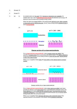
3. (a) (i) As isolated atoms are far apart, their interatomic interactions are negligible. An
isolated atom has a set of well-defined energy levels that electrons can occupy. All
electrons have the same set of possible energy values
When the atoms are closer together, the energy levels split and curve, either upwards
or downwards and by varying amounts. Hence, these energy-levels combine to form a
set of energy-bands.
(ii)
For a p-type extrinsic semiconductor, when acceptor atoms are added, they
provide an acceptor level which is just above the valence band. The valence electrons
of the pure semiconductor can be easily excited to jump into this level, leaving behind
a hole in the valence band.
When a p.d. is applied, these holes will move within in the valence band to conduct
current.
For a n-type extrinsic semiconductor, when donor atoms are added, each atom
provides an electron in the donor level which is just below the conduction band. The
donor electron can easily jump into the conduction band, thus becoming one of the
conduction electrons to move freely through the semiconductor (by occupying higher
energy levels within the conduction band).
When a p.d. is applied, these electrons will move in the conduction band in the
opposite direction to the direction of the electric field to produce current flow.
2. (iii) 1. Each p- and n-type semiconductor is electrically neutral.
Due to concentration gradient, the mobile electrons from the n-side and the mobile
holes from the p-side flow across the junction and combine (no need to apply p.d.).
This process leaves the n-side with a positive charge layer, and the p-side with a
negative charge layer.
The positive and negative charge layers on the 2 sides of the junction set up an
electric field E in the junction. This electric field prevents any further movement of
charge from the n-side and p-side across the junction. Hence, a depletion layer is
formed.
Gave the correct direction of motion of charges to create region depleted of charges.
Understand that the e- and holes built up in p and n region creates internal E-field to
prevent further movement of charges
2. When a p.d. is applied across the device in Fig. 7, the width of the depletion layer can
be varied.
To allow subsequent charges to flow across the depletion layer, positive terminal of
voltage supply is applied to p-side and negative terminal to n-side to produce a narrow
depletion layer (→ rectifier in forward biased)
or
To prevent subsequent charges from flowing across the depletion layer, positive
terminal of voltage supply is applied to n-side and negative terminal to p-side to
produce a wider depletion layer (→ rectifier in reverse biased).
The rectifier, then is unidirectional as it only allows current to flow through it in one
direction. (Diodes can convert an ac voltage into a dc voltage)
Explain correctly that forward bias lead to decrease in depletion width
Explain correctly that reverse bias lead to increase in depletion width
4. Answer: B
5. Answer: D
6. Answer: B
Electrons and holes are urged towards the junction region when the diode is in forward bias. This results
in the reduction of the depletion region, thus allowing a current to flow.
7. No answer given
8. No answer given
9. (a) Power per unit area = 3.0 x 10
-3
/ 1.0 x 10
-9
/ 8 x 10
-10
W m
-2
(b) When more atoms are in an upper state than in a lower state, population inversion occurs.
Population inversion is a necessary condition for stimulated emission (amplification) to
dominate or laser action to occur. Light and electricity are commonly used to selectively
transfer energy to atoms or molecules, exciting them to higher energy levels, most of the time,
a metastable state.
The photon that any atom releases has a certain wavelength that is dependent on the energy
difference between the excited state and the ground state. If this photon (possessing a certain
energy and phase) should encounter another atom that has an electron in the same excited
state, stimulated emission can occur. The first photon can stimulate or induce atomic emission
3. such that the subsequent emitted photon (from the second atom) vibrates with the same
frequency and direction as the incoming photon.
When a stimulated emission happens, one photon results in two in-phase photons.
The other key to a laser is a pair of mirrors, one at each end of the lasing medium. Photons,
with a very specific frequency and phase, reflect off the mirrors to travel back and forth through
the lasing medium. In the process, they stimulate other electrons to make the downward
energy jump and can cause the emission of more photons of the same frequency and phase.
The initial two in-phase photons will create two simulated emissions, resulting in four in-phase
photons and so on. A cascade effect occurs, and soon we have propagated many, many
photons of the same frequency (energy) and in exactly the same direction in phase with the
incident photon (conservation of momentum). Thus, the light is amplified, resulting in an
intense (high intensity) and directed (same direction in phase) light beam.
10. (a)
An incident photon of energy equal or larger than the band gap energy can excite an electron
from the valence band into the conduction band, resulting in a electron in the conduction band
and a hole in the valence band.
(b),(c),(d)
11. Answer: B
Laser Light is highly coherent but it is an electromagnetic wave and will undergo diffraction when
passing through a small aperture.
12. Answer: D
Both types of charge carriers are present. The majority charge carriers are holes and the minority
electrons.
4. 13. (a) (i) 1. Metastable state is a long-lived excited state. The energy level is said to be
a metastable state when an excited atom remains in this state for a relatively
longtime (~10
-3
s) before falling to the ground state. [B1]
2. Population inversion is a condition when the higher of the two states has
more atoms in excited states than the lower state (or ground state). [B1]
(ii) At equilibrium, the number of atoms in the excited state equal to the number of atoms
in the ground state. For lasing to occur, number of atoms in the excited state must be
greater than the ground state (non-equilibrium condition) [C1]
The largest number of atoms that can undergo stimulated emission is
[C1]
Total energy in a single pulse of laser [A1]
(iii) Power = rate of photon arrival x energy of photon
Rate of photon arrival, [C1]
no of photons emitted per minute = [M1]
[A1]
(iv) [M1]
Diameter of laser beam [M1]
[C1]
[A1]
(b) (i) Two separate diagrams showing clearly the conduction bands, valence bands (for
metal and semiconductor) and the difference in energy gap in the forbidden band.
For metal, the conduction band overlaps with the valence band. The region of overlap
has free electrons and there is no energy gap between the conduction and valence
bands. When a potential difference is applied, conduction of electricity in the metal is
readily possible because of the availability of free electrons in the conduction band.
[B1]
5. For semiconductor, there is a small energy gap between the conduction and valence
bands. At 0 Kelvin or absolute zero, there is no free electron in the conduction band.
With a rise in temperature, some electrons can made to be excited into the conduction
band resulting in an increase in current conductivity or a decrease in resistivity. Thus,
electric current conduction in a semiconductor is smaller than that of metal and it
increases with temperature. [B1]
(ii) Diagram to show how free charge-carriers, electrons in this case, are created due to
the introduction of donor atoms. [B1]
Intrinsic semiconductor is made from an element with 4 electrons in the outermost
shell (eg silicon). The outermost electrons readily paired up with neighbouring
electrons. [B1]
When donor atoms (eg antimony, a Group 5 element) are introduced (doped) into the
semiconductor, lone (unattached) electrons are created. [B1]
These unpaired electrons are the free negative charge carriers in the n-type
semiconductor and are the main agents for electric current conduction.
[B1]
Alternative answer
In terms of the band theory, the donor atoms introduce an energy level (called donor
level) just beneath the conduction band. As the energy gap now is smaller, more
electrons are able to enter the conduction band resulting in an increased conductivity
for n-type semiconductor. N-type semiconductor has more electrons than holes as
free charge carriers.
14. Answer: C
In stimulated emission, the photon that is created by the transition of a electron from an excited state to
a lower energy level must have the same energy and phase as the incoming photon.
15. Answer: D
Some transitions are spontaneous; stimulated emissions increase the intensity of the laser beam and
are desirable but not crucial for its production.
6. 16. (a) (i) Difference in energy levels = hc/ ג
= [6.63 x 10
-34
x 3 x 10
8
]/(193 x 10
-9
)
= 1.03 x 10
-18
J / 6.44 eV
(ii) N = (1.58 x 10
-13
)/ (1.03 x 10
-18
J)
= 1.53 x 10
5
(b) For Si : energy gap = hf = 6.63 x 10
-34
x 2.75 x 10
14
= 1.82 x 10
-19
J/1.14 eV
For Ge : energy gap = hf = 6.63 x 10
-34
x 1.79 x 10
14
= 1.19 x 10
-19
J/0.742 eV
(c) Diffusion allows electrons from the N-type semiconductor and holes from the P-type
semiconductor to meet and recombine near the junction, forming +ve and −ve ions.
Electric field set up by these ions opposes further electron-hole recombination, hence
forming the depletion zone.
(d) (i)
Substituting values into above,
(ii)
17. Answer: A
The presence of impurities in a semiconductor increases the conductivity which mean decreases the
resistance.
18. Answer: C
Under reverse bias mode, the electrons in the n-region are pulled away from the depletion region,
leaving more immobile positive ions in the region. In other words, the electrons are driven towards the n-
region
19. (a) X – intrinsic semiconductor
Y – metal
(b) Y conducts electricity at 0K
As the empty conduction bands overlap with valence bands containing electrons, hence the
electrons can move to a higher energy level with little or no additional energy imparted.
(Mentioning ‘free electrons’ without reference to the overlap of bands will not be awarded any
credit.)
(c) 1] for any 3 of the following points:
At higher temperatures, an electron may gain enough energy to move from the valence band to
the conduction band leaving behind a vacant site known as the hole, in the otherwise filled
valence band.
This hole acts as a positive charge carrier as a free electron from a nearby site can then move
into the hole.
Whenever an electron does so, it creates a new hole at the site it abandoned. The net effect
will be viewed as the hole moving in opposite direction to the movement of the electron.
These movements of holes and electrons give rise to a current in the same direction when an
external electric field is applied. Electrons conduct in the conduction band, while holes conduct
in the valence band.
7. 20. Answer not provided
21. Answer not provided
22. Answer not provided
23. Answer not provided
24. (a) (i) The meta-stable state is a long-lived excited state where the electrons/atoms can exist for a relatively
long time.
(ii) Electrons are excited by an external source to E3 where they quickly de-excite to either E1 or E2 states.
Those that are de-excited to the ground state will be excited by the external source again. Since E2 is a
meta-stable state in time to come, most electrons will be accumulated in that level compared to the ground
state. Thus, population inversion has occurred. If an electron in E2 manages to undergo spontaneous
emission to produce a photon of energy E2 – E1, the photon will be able to stimulate other electrons in the
meta-stable state to de-excite and produce more photons. Through stimulated emission, more photons will
be produced, which all have the same wavelength, same phase and travelling in the same direction. Thus,
the production of laser.
(iii) For the three-level laser system, the photons produced by stimulated emission may be re-absorbed by
the electrons in the ground state and this reduces the emission of the photons necessary for lasing.
For the four-level laser system, the electrons will de-excite quickly from E2 – E1 , and
will not re-absorb the photons necessary for lasing (E3 – E2) since E2 is a short-lived state.
(b) (i)
(ii) For n-type doping, a donor level is created near to the conduction band with a much smaller bandgap. At
room temperature, the electrons at the donor level will be able to excite to the conduction band through
thermal agitation. Hence, conductivity increases.
(iii) The majority of the charge carriers for n- and p-type semiconductors are electrons and holes respectively.
25. Answer: B
26. Answer: D
27. Answer: D
28. Answer: A
29. (a) (i)
8. (ii) Metastable state, population inversion, stimulated emission.
(b) (i) P-type
(ii) Berryllium is in Group II and has 2 valence electrons which is fewer than in gallium, aluminium and
arsenic. Doping with beryllium will introduce holes in the bonds in the valence band which are otherwise
fully occupied.
With a small amount of energy, neighbouring electrons are able to break away to fill a hole, leaving a
hole in the previous bond (or holes are the majority charge carriers in the valence band).
30. (a)
(b) (i) At room temperature (~300 K), the thermal energy of the electron is ~0.01 eV. This is too
compared with the band gap of 1.1 eV.
Hence only a very small number of electrons can be thermally excited from the top of valence band
to the bottom of the conduction band.
(ii) Fermi-Dirac distribution
Since the Fermi level is about midway between EC and EV, the difference in energy between energy
states in the conduction band and Fermi energy (~0.5 eV) is very much larger than at room
temperature (~0.01 eV), i.e.,
9. (iii)
(iv) The number density of electrons in the conduction band
(v) The number density of electrons in the conduction band ne at room temperature
1.5 x 10
16
m
-3
.
31. Answer: B
10. 32. (a) Stimulated emission releases a second photon with the same frequency. Accounts for why laser light is
monochromatic.
The emitted photon is in phase with the original photon. Accounts for why laser light is coherent.
Emitted photon travels in the same direction as the original photon. Accounts for why laser light is
collimated/ highly directional.
(b) Atoms from the ground state E1 are ‘pumped’ up to an excited state E3 – for example, by the
absorption of energy from intense light source that surrounds the lasing material.
From E3, the atoms decay rapidly to a state of energy E2. For lasing to occur this state must be
metastable: that is it must have a relatively long mean life against decay by spontaneous emission.
State E2 then become more heavily populated than state E1, thus providing the necessary population
inversion.
An incident photon can then trigger an avalanche of emission by stimulated emission, resulting in the
production of laser light. This is achieved by using two mirrors, one 100% reflecting and the other 99%.
(c) Due to high concentration of electrons, the electrons in the n-type semiconductor start to diffuse into
the p-type semiconductor and the holes start to diffuse into the n-type semiconductor.
The electrons which have diffused into the p-type semiconductor will then combine with the hole there
while the holes which have been diffused into the n-type semiconductor will combine with the electrons.
This results in the formation of a depletion zone.
Under reverse bias condition, the width of the depletion layer will increase.
33 (a) A laser beam’s power is incident on a smaller area and thus more intense.
A laser beam’s radiation energy is in the visible spectrum whereas a filament lamp radiates
energy in the invisible spectrum as well.
[1]
[1]
(b)
Clearly labelled valence, conduction bands and small band gap.
Indicating bands are almost empty/filled OR carriers in the bands.
[1]
[1]
(c) The addition of boron which has only 3 valence electrons introduces available vacant
energy levels very close to the top of the valence band.
Electrons in the valence band can easily be thermally agitated to fill the acceptor energy
level, creating holes in the valence band.
[1]
[1]
(1.1 eV)
11. 34. Answers not provided
35. Answers not provided
36. Answers not provided
37. Answers not provided
38. Answer: C
39. Answer: A
40. (c) All photons produced by stimulated emission in a laser have the same phase difference,
whereas those produced by spontaneous emission do not.
Thus for a double-slit experiment, light from a single laser source incident (directly) on the double slits
will produce an interference pattern.