

Empfohlen
Weitere ähnliche Inhalte
Was ist angesagt?
Was ist angesagt? (20)
Andere mochten auch
Andere mochten auch (12)
Ähnlich wie nota K pcb
Ähnlich wie nota K pcb (20)
Mehr von mkazree
Mehr von mkazree (20)
nota K pcb
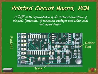
- 1. Printed Circuit Board, PCB A PCB is the representation of the electrical connections of the pads (footprints) of component packages with solder pads and signal tracks. Footprint Solder Pad Track
- 2. PCB Materials Conducting layers are typically made of thin copper foil. Insulating layers dielectric are typically laminated together with epoxy resin prepreg. The board is typically coated with a solder mask that is green in color . Type of prepreg: FR-2 (Phenolic cotton paper), FR-3 (Cotton paper and epoxy), FR-4 (Woven glass and epoxy), FR-5 (Woven glass and epoxy), FR-6 (Matte glass and polyester), G-10 (Woven glass and epoxy), CEM-1 (Cotton paper and epoxy), CEM-2 (Cotton paper and epoxy), CEM-3 (Woven glass and epoxy), CEM-4 (Woven glass and epoxy), CEM-5 (Woven glass and polyester FR-4 is most common material used today
- 3. Component Footprint Define as: • The pattern and space on a board taken up by a component • A graphic software representation of a component. Categorized into: 1. Thru hole device – Axial-leaded – Radial-leaded 2. Surface Mount device
- 4. Radial-leaded Capacitor Layout footprint Axial-leaded Resistor Layout footprint
- 5. Component Package • A type of PCB component which contains a chip and acts to make a convenient mechanism for protecting the chip while on the shelf and after attachment to a PCB. • With its leads soldered to a printed circuit board, a package serves as the electrical conduction interface between the chip and the board.
- 6. TO-92 TO-220 DIP8 DO-41
- 7. Airwire / Ratnest • Airwires are to be seen only in the layout view (PCB). • They represent the electrical connections (signals) between pads and often intersect each other. • They are disentangled later by the use routing. A multitude of airwires are called ratsnest. • “rat's nest” is used to describe a particularly messy or disordered environment.
- 8. Multitude airwires create disorderly environment, commonly called as ratnest Air-wire
- 9. Component Placement Guideline • place components close to each other while trying to keep the routing process in mind. – As you place components, turn and flip each one around to make the guide lines as straight and as short as possible. X √
- 10. Guideline (cont.) • place components on the circuit board just like they are drawn on the schematic. – That means that components that are directly connected to each other will be placed closely together. • It is usually easiest to place the big components first (like microcontrollers, op amps, etc.) and then place all of the little ones that connect to them (resistors, capacitors, etc.) around them. Schematic Layout
- 11. Guideline (cont.) • completely place all components on the circuit board before beginning any routing. • try to leave at least 30 mils between components, and 50 mils between a component and the edge of the circuit board. Mil? a unit of distance equal to 0.001 inch: a "milli-inch," One mil is exactly 25.4 microns. 50 mils 30 mils 1 mil = 1/1000 inch
- 12. Routing Routing is the process of selecting paths in a net to connect components according to its connection. Guideline • In general, the shortest routes are the best. – This is because long routes tend to generate more electrical noise, or pick up more electrical noise.
- 13. Guideline (Grounding) • Ground is the most important signal on all circuit boards • In a well-grounded board, the ground signal is a solid reference for every signal on the board • ground net with very narrow traces, it will have higher resistance than if you route it with wide traces • At high frequencies, a wide trace is less inductive than a narrow one. – This means that the high frequency AC resistance of your ground is lower. • Conclusion: ground must be route using wide traces
- 14. Power Plane • To achieve better grounding cooper pouring and power plane for ground route is introduced. • Benefit of abundance grounding: – to provide built-in shielding from external interference – help quiet any noisy routes – reduce cross coupling on the board. – provides a good safe path for static electricity, thus increasing the reliability of your finished board
- 15. Ground Routing Ground Plane a.k.a Copper Pouring
- 16. Thermal Relief • A thermal relief pad is a PCB pad connected to a copper pour using a thermal connection. • It looks like a normal pad with copper "spokes" connecting it to the surrounding copper. • A pad directly connected to the copper pour would be difficult to solder, since the heat provided by the soldering iron will quickly leak away from the pad and into the copper pour (due to high thermal conductivity of copper). • A thermal connection restricts the heat flow, making the pad easier to solder.
- 17. Thermal Relief Solder pad on cooper pouring. Relief heat transfer to ease soldering