SlideShare ist ein Scribd-Unternehmen logo
1 von 22
Downloaden Sie, um offline zu lesen
LM2907/LM2917 Frequency to Voltage Converter
                                                                                                               December 9, 2008


 LM2907/LM2917
 Frequency to Voltage Converter
 General Description                                                 ■ Only one RC network provides frequency doubling
                                                                     ■ Zener regulator on chip allows accurate and stable
 The LM2907, LM2917 series are monolithic frequency to volt-             frequency to voltage or current conversion (LM2917)
 age converters with a high gain op amp/comparator designed
 to operate a relay, lamp, or other load when the input fre-
 quency reaches or exceeds a selected rate. The tachometer
                                                                     Features
 uses a charge pump technique and offers frequency doubling          ■ Ground referenced tachometer input interfaces directly
 for low ripple, full input protection in two versions (LM2907-8,        with variable reluctance magnetic pickups
 LM2917-8) and its output swings to ground for a zero fre-           ■ Op amp/comparator has floating transistor output
 quency input.                                                       ■ 50 mA sink or source to operate relays, solenoids, meters,
 The op amp/comparator is fully compatible with the tachome-             or LEDs
 ter and has a floating transistor as its output. This feature       ■ Frequency doubling for low ripple
 allows either a ground or supply referred load of up to 50 mA.
 The collector may be taken above VCC up to a maximum
                                                                     ■ Tachometer has built-in hysteresis with either differential
                                                                         input or ground referenced input
 VCE of 28V.
                                                                     ■ Built-in zener on LM2917
 The two basic configurations offered include an 8-pin device
 with a ground referenced tachometer input and an internal           ■ ±0.3% linearity typical
 connection between the tachometer output and the op amp             ■ Ground referenced tachometer is fully protected from
 non-inverting input. This version is well suited for single speed       damage due to swings above VCC and below ground
 or frequency switching or fully buffered frequency to voltage
 conversion applications.                                            Applications
 The more versatile configurations provide differential              ■   Over/under speed sensing
 tachometer input and uncommitted op amp inputs. With this
 version the tachometer input may be floated and the op amp
                                                                     ■   Frequency to voltage conversion (tachometer)
 becomes suitable for active filter conditioning of the tachome-     ■   Speedometers
 ter output.                                                         ■   Breaker point dwell meters
 Both of these configurations are available with an active shunt     ■   Hand-held tachometer
 regulator connected across the power leads. The regulator           ■   Speed governors
 clamps the supply such that stable frequency to voltage and
                                                                     ■   Cruise control
 frequency to current operations are possible with any supply
 voltage and a suitable resistor.                                    ■   Automotive door lock control
                                                                     ■   Clutch control
 Advantages                                                          ■   Horn control

 ■ Output swings to ground for zero frequency input                  ■   Touch or sound switches

 ■ Easy to use; VOUT = fIN × VCC × R1 × C1


 Connection Diagrams
 Dual-In-Line and Small Outline Packages, Top Views


                                                      794201                                                         794202
           Order Number LM2907M-8 or LM2907N-8                               Order Number LM2917M-8 or LM2917N-8
           See NS Package Number M08A or N08E                                See NS Package Number M08A or N08E

© 2008 National Semiconductor Corporation   7942                                                                     www.national.com
LM2907/LM2917


                                                                794203                                             794204
                              Order Number LM2907M or LM2907N                       Order Number LM2917M or LM2917N
                             See NS Package Number M14A or N14A                    See NS Package Number M14A or N14A


                   Ordering Information
                             Order              Package                  Package             Package             Supplied
                            Number               Type                    Number              Marking               As
                          LM2907M-8         8-Pin SOIC Narrow             M08A              LM2907M-8            Rail of 95
                         LM2907MX-8         8-Pin SOIC Narrow             M08A              LM2907M-8           Reel of 2500
                           LM2907M         14-Pin SOIC Narrow             M14A               LM2907M             Rail of 55
                          LM2907MX         14-Pin SOIC Narrow             M14A               LM2907M            Reel of 2500
                          LM2907N-8         8-Pin Molded DIP              N08E              LM2907N-8            Rail of 40
                           LM2907N          14-Pin Molded DIP             N14A               LM2907N             Rail of 25
                          LM2917M-8         8-Pin SOIC Narrow             M08A              LM2917M-8            Rail of 95
                         LM2917MX-8         8-Pin SOIC Narrow             M08A              LM2917M-8           Reel of 2500
                           LM2917M         14-Pin SOIC Narrow             M14A               LM2917M             Rail of 55
                          LM2917MX         14-Pin SOIC Narrow             M14A               LM2917M            Reel of 2500
                          LM2917N-8         8-Pin Molded DIP              N08E              LM2917N-8            Rail of 40
                           LM2917N          14-Pin Molded DIP             N14A               LM2917N             Rail of 25


                www.national.com                                            2
LM2907/LM2917
     Absolute Maximum Ratings (Note 1)                                                          Op Amp/Comparator                                  0.0V to +28V
                                                                                              Power Dissipation
     If Military/Aerospace specified devices are required,
     please contact the National Semiconductor Sales Office/                                    LM2907-8, LM2917-8                                     1200 mW
     Distributors for availability and specifications.                                          LM2907-14, LM2917-14                                   1580 mW
                                                                                                See (Note 1)
      Supply Voltage                                                       28V
                                                                                              Operating Temperature Range                      −40°C to +85°C
      Supply Current (Zener Options)                                     25 mA
                                                                                              Storage Temperature Range                       −65°C to +150°C
      Collector Voltage                                                    28V
                                                                                              Soldering Information
      Differential Input Voltage
                                                                                                Dual-In-Line Package
        Tachometer                                                          28V
                                                                                                  Soldering (10 seconds)                                    260°C
        Op Amp/Comparator                                                   28V
                                                                                                Small Outline Package
      Input Voltage Range
                                                                                                  Vapor Phase (60 seconds)                                  215°C
        Tachometer
                                                                                                  Infrared (15 seconds)                                     220°C
           LM2907-8, LM2917-8                                           ±28V
           LM2907, LM2917                                       0.0V to +28V

     Electrical Characteristics
     VCC = 12 VDC, TA = 25°C, see test circuit
 Symbol                        Parameter                                           Conditions                          Min        Typ          Max            Units
TACHOMETER
                 Input Thresholds                            VIN = 250 mVp-p @ 1 kHz (Note 2)                          ±10        ±25           ±40            mV
                 Hysteresis                                  VIN = 250 mVp-p @ 1 kHz (Note 2)                                      30                          mV
                 Offset Voltage                              VIN = 250 mVp-p @ 1 kHz (Note 2)
                    LM2907/LM2917                                                                                                  3.5           10            mV
                    LM2907-8/LM2917-8                                                                                               5            15            mV
                 Input Bias Current                          VIN = ±50 mVDC                                                        0.1           1              μA
VOH              Pin 2                                       VIN = +125 mVDC (Note 3)                                              8.3                           V
VOL              Pin 2                                       VIN = −125 mVDC (Note 3)                                              2.3                           V
I2, I3           Output Current                              V2 = V3 = 6.0V (Note 4)                                   140        180           240             μA
I3               Leakage Current                             I2 = 0, V3 = 0                                                                     0.1             μA
K                Gain Constant                               (Note 3)                                                   0.9        1.0          1.1
                 Linearity                                   fIN = 1 kHz, 5 kHz, 10 kHz (Note 5)                       −1.0        0.3         +1.0             %
OP/AMP COMPARATOR
VOS                                                          VIN = 6.0V                                                             3            10            mV
IBIAS                                                        VIN = 6.0V                                                            50           500             nA
                 Input Common-Mode Voltage                                                                               0                  VCC−1.5V             V
                 Voltage Gain                                                                                                     200                         V/mV
                 Output Sink Current                         VC = 1.0                                                   40         50                          mA
                 Output Source Current                       VE = VCC −2.0                                                         10                          mA
                 Saturation Voltage                          ISINK = 5 mA                                                          0.1          0.5              V
                                                             ISINK = 20 mA                                                                      1.0              V
                                                             ISINK = 50 mA                                                         1.0          1.5              V
ZENER REGULATOR
                 Regulator Voltage                           RDROP = 470Ω                                                         7.56                           V
                 Series Resistance                                                                                                10.5           15           Ω
                 Temperature Stability                                                                                             +1                        mV/°C
                 Total Supply Current                                                                                              3.8           6             mA

     Note 1: For operation in ambient temperatures above 25°C, the device must be derated based on a 150°C maximum junction temperature and a thermal resistance
     of 101°C/W junction to ambient for LM2907-8 and LM2917-8, and 79°C/W junction to ambient for LM2907-14 and LM2917-14.
     Note 2: Hysteresis is the sum +VTH − (−VTH), offset voltage is their difference. See test circuit.
     Note 3: VOH is equal to ¾ × VCC − 1 VBE, VOL is equal to ¼ × VCC − 1 VBE therefore VOH − VOL = VCC/2. The difference, VOH − VOL, and the mirror gain, I2/I3, are
     the two factors that cause the tachometer gain constant to vary from 1.0.
     Note 4: Be sure when choosing the time constant R1 × C1 that R1 is such that the maximum anticipated output voltage at pin 3 can be reached with I3 × R1. The
     maximum value for R1 is limited by the output resistance of pin 3 which is greater than 10 MΩ typically.


                                                                                       3                                                              www.national.com
LM2907/LM2917      Note 5: Nonlinearity is defined as the deviation of VOUT (@ pin 3) for fIN = 5 kHz from a straight line defined by the VOUT @ 1 kHz and VOUT @ 10 kHz. C1 =
                   1000 pF, R1 = 68k and C2 = 0.22 mFd.


                   Test Circuit and Waveform


                                                                                                                                     794206

                                                                      Tachometer Input Threshold Measurement


                                                                                                                                      794207


                www.national.com                                                                 4
LM2907/LM2917
Typical Performance Characteristics
             Tachometer Linearity                      Tachometer Linearity
               vs Temperature                            vs Temperature


                                    794246                                    794247


             Total Supply Current                        Zener Voltage vs
                                                           Temperature


                                    794240

                                                                              794241


       Normalized Tachometer Output (K)          Normalized Tachometer Output (K)
                vs Temperature                            vs Temperature


                                    794242                                    794243


                                             5                                         www.national.com
LM2907/LM2917
                                   Tachometer Currents I2and I3                Tachometer Currents I2and I3
                                       vs Supply Voltage                            vs Temperature


                                                                  794244                                     794245


                                   Tachometer Linearity vs R1                  Tachometer Input Hysteresis
                                                                                    vs Temperature


                                                                  794248
                                                                                                           794249


                                    Op Amp Output Transistor                    Op Amp Output Transistor
                                        Characteristics                             Characteristics


                                                                                                           794251
                                                                  794250


                www.national.com                                           6
LM2907/LM2917
                                                                          The size of C2 is dependent only on the amount of ripple volt-
Applications Information                                                  age allowable and the required response time.
The LM2907 series of tachometer circuits is designed for
minimum external part count applications and maximum ver-                 CHOOSING R1 AND C1
satility. In order to fully exploit its features and advantages           There are some limitations on the choice of R1 and C1 which
let's examine its theory of operation. The first stage of oper-           should be considered for optimum performance. The timing
ation is a differential amplifier driving a positive feedback flip-       capacitor also provides internal compensation for the charge
flop circuit. The input threshold voltage is the amount of                pump and should be kept larger than 500 pF for very accurate
differential input voltage at which the output of this stage              operation. Smaller values can cause an error current on R1,
changes state. Two options (LM2907-8, LM2917-8) have one                  especially at low temperatures. Several considerations must
input internally grounded so that an input signal must swing              be met when choosing R1. The output current at pin 3 is in-
above and below ground and exceed the input thresholds to                 ternally fixed and therefore VO/R1 must be less than or equal
produce an output. This is offered specifically for magnetic              to this value. If R1 is too large, it can become a significant
variable reluctance pickups which typically provide a single-             fraction of the output impedance at pin 3 which degrades lin-
ended ac output. This single input is also fully protected                earity. Also output ripple voltage must be considered and the
against voltage swings to ±28V, which are easily attained with            size of C2 is affected by R1. An expression that describes the
these types of pickups.                                                   ripple content on pin 3 for a single R1C2 combination is:
The differential input options (LM2907, LM2917) give the user
the option of setting his own input switching level and still have
the hysteresis around that level for excellent noise rejection
in any application. Of course in order to allow the inputs to
attain common-mode voltages above ground, input protection
is removed and neither input should be taken outside the lim-             It appears R1 can be chosen independent of ripple, however
its of the supply voltage being used. It is very important that           response time, or the time it takes VOUT to stabilize at a new
an input not go below ground without some resistance in its               voltage increases as the size of C2 increases, so a compro-
lead to limit the current that will then flow in the epi-substrate        mise between ripple, response time, and linearity must be
diode.                                                                    chosen carefully.
Following the input stage is the charge pump where the input              As a final consideration, the maximum attainable input fre-
frequency is converted to a dc voltage. To do this requires               quency is determined by VCC, C1 and I2:
one timing capacitor, one output resistor, and an integrating
or filter capacitor. When the input stage changes state (due
to a suitable zero crossing or differential voltage on the input)
the timing capacitor is either charged or discharged linearly
between two voltages whose difference is VCC/2. Then in one               USING ZENER REGULATED OPTIONS (LM2917)
half cycle of the input frequency or a time equal to 1/2 fIN the
change in charge on the timing capacitor is equal to VCC/2 ×              For those applications where an output voltage or current
C1. The average amount of current pumped into or out of the               must be obtained independent of supply voltage variations,
capacitor then is:                                                        the LM2917 is offered. The most important consideration in
                                                                          choosing a dropping resistor from the unregulated supply to
                                                                          the device is that the tachometer and op amp circuitry alone
                                                                          require about 3 mA at the voltage level provided by the zener.
                                                                          At low supply voltages there must be some current flowing in
                                                                          the resistor above the 3 mA circuit current to operate the reg-
The output circuit mirrors this current very accurately into the          ulator. As an example, if the raw supply varies from 9V to 16V,
load resistor R1, connected to ground, such that if the pulses            a resistance of 470Ω will minimize the zener voltage variation
of current are integrated with a filter capacitor, then VO = ic ×         to 160 mV. If the resistance goes under 400Ω or over 600Ω
R1, and the total conversion equation becomes:                            the zener variation quickly rises above 200 mV for the same
                 VO = VCC × fIN × C1 × R1 × K                             input variation.

Where K is the gain constant—typically 1.0.


                                                                      7                                                     www.national.com
LM2907/LM2917
                   Typical Applications
                                                 Minimum Component Tachometer


                                                                                                           794208


                                      ”Speed Switch”, Load is Energized when fIN ≥ (1 / ( 2RC))


                                                                                                  794209


                www.national.com                                 8
LM2907/LM2917
Zener Regulated Frequency to Voltage Converter


                                                 794210

          Breaker Point Dwell Meter


                                                          794211


                      9                                            www.national.com
LM2907/LM2917                          Voltage Driven Meter Indicating Engine RPM
                                    VO = 6V @ 400 Hz or 6000 ERPM (8 Cylinder Engine)


                                                                                                   794212

                                         Current Driven Meter Indicating Engine RPM
                                   IO = 10 mA @ 300 Hz or 6000 ERPM (6 Cylinder Engine)


                                                                                          794213


                www.national.com                            10
LM2907/LM2917
         Capacitance Meter
VOUT = 1V–10V for CX = 0.01 to 0.1 mFd
             (R = 111k)


                                         794214

   Two-Wire Remote Speed Switch


                                                  794215


                  11                                       www.national.com
LM2907/LM2917                                                    100 Cycle Delay Switch


                                                                                          794216


                   Variable Reluctance Magnetic Pickup Buffer Circuits


                                                                     794239
                                                                                                   794217
                   Precision two-shot output frequency
                   equals twice input frequency.


                   Pulse height = VZENER


                www.national.com                                              12
LM2907/LM2917
Finger Touch or Contact Switch


                                                                                        794219


                                                          794218


                                            Flashing LED Indicates Overspeed


                                                                               794220
Flashing begins when fIN ≥ 100 Hz.
Flash rate increases with input frequency
increase beyond trip point.


                                                           13                                    www.national.com
LM2907/LM2917                        Frequency to Voltage Converter with 2 Pole Butterworth Filter to Reduce Ripple


                                                                                                     794221


                   Overspeed Latch


                                                                                                                      794223


                                                               794222


                www.national.com                                           14
LM2907/LM2917
Some Frequency Switch Applications May Require Hysteresis in the
Comparator Function Which can be Implemented in Several Ways


                                                                   794224


                                              794225
                                                                             794226


                                     794227
                                                                            794228


                                                       15                            www.national.com
LM2907/LM2917      Changing the Output Voltage for an Input Frequency of Zero


                                                                                           794230


                                                                        794229


                   Changing Tachometer Gain Curve or Clamping the Minimum Output Voltage


                                                                                                    794232


                                                               794231


                www.national.com                                                 16
LM2907/LM2917
Anti-Skid Circuit Functions
“Select-Low” Circuit


                                                                                        794234
                                                         VOUT is proportional to the lower
                                                          of the two input wheel speeds.


                                        794233


“Select-High” Circuit


                                                                                       794236
                                                         VOUT is proportional to the higher
                                                          of the two input wheel speeds.


                                        794235


                              “Select-Average” Circuit


                                                                              794237


                                         17                                                      www.national.com
LM2907/LM2917


www.national.com
                                                                                            Equivalent Schematic Diagram


18
                                                                          794238
                   *This connection made on LM2907-8 and LM2917-8 only.
                   **This connection made on LM2917 and LM2917-8 only.
LM2907/LM2917
Physical Dimensions inches (millimeters) unless otherwise noted


                         8-Lead (0.150″ Wide) Molded Small Outline Package, JEDEC
                                  Order Number LM2907M-8 or LM2917M-8
                                         NS Package Number M08A


                                                    19                              www.national.com
LM2907/LM2917


                                          Molded SO Package (M)
                                    Order Number LM2907M or LM2917M
                                        NS Package Number M14A


                                      Molded Dual-In-Line Package (N)
                                   Order Number LM2907N-8 or LM2917N-8
                                         NS Package Number N08E


                www.national.com                   20
LM2907/LM2917
 Molded Dual-In-Line Package (N)
Order Number LM2907N or LM2917N
    NS Package Number N14A


               21                  www.national.com
LM2907/LM2917 Frequency to Voltage Converter
                                                                                                                         Notes


                                                For more National Semiconductor product information and proven design tools, visit the following Web sites at:

                                                                                    Products                                                              Design Support
                                                 Amplifiers                                www.national.com/amplifiers           WEBENCH® Tools                www.national.com/webench
                                                 Audio                                     www.national.com/audio                App Notes                     www.national.com/appnotes
                                                 Clock and Timing                          www.national.com/timing               Reference Designs             www.national.com/refdesigns
                                                 Data Converters                           www.national.com/adc                  Samples                       www.national.com/samples
                                                 Interface                                 www.national.com/interface            Eval Boards                   www.national.com/evalboards
                                                 LVDS                                      www.national.com/lvds                 Packaging                     www.national.com/packaging
                                                 Power Management                          www.national.com/power                Green Compliance              www.national.com/quality/green
                                                       Switching Regulators                www.national.com/switchers            Distributors                  www.national.com/contacts
                                                       LDOs                                www.national.com/ldo                  Quality and Reliability       www.national.com/quality
                                                       LED Lighting                        www.national.com/led                  Feedback/Support              www.national.com/feedback
                                                       Voltage Reference                   www.national.com/vref                 Design Made Easy              www.national.com/easy
                                                 PowerWise® Solutions                      www.national.com/powerwise            Solutions                     www.national.com/solutions
                                                 Serial Digital Interface (SDI)            www.national.com/sdi                  Mil/Aero                      www.national.com/milaero
                                                 Temperature Sensors                       www.national.com/tempsensors          Solar Magic®                  www.national.com/solarmagic
                                                 Wireless (PLL/VCO)                        www.national.com/wireless             Analog University®            www.national.com/AU

                                                 THE CONTENTS OF THIS DOCUMENT ARE PROVIDED IN CONNECTION WITH NATIONAL SEMICONDUCTOR CORPORATION
                                                 (“NATIONAL”) PRODUCTS. NATIONAL MAKES NO REPRESENTATIONS OR WARRANTIES WITH RESPECT TO THE ACCURACY
                                                 OR COMPLETENESS OF THE CONTENTS OF THIS PUBLICATION AND RESERVES THE RIGHT TO MAKE CHANGES TO
                                                 SPECIFICATIONS AND PRODUCT DESCRIPTIONS AT ANY TIME WITHOUT NOTICE. NO LICENSE, WHETHER EXPRESS,
                                                 IMPLIED, ARISING BY ESTOPPEL OR OTHERWISE, TO ANY INTELLECTUAL PROPERTY RIGHTS IS GRANTED BY THIS
                                                 DOCUMENT.
                                                 TESTING AND OTHER QUALITY CONTROLS ARE USED TO THE EXTENT NATIONAL DEEMS NECESSARY TO SUPPORT
                                                 NATIONAL’S PRODUCT WARRANTY. EXCEPT WHERE MANDATED BY GOVERNMENT REQUIREMENTS, TESTING OF ALL
                                                 PARAMETERS OF EACH PRODUCT IS NOT NECESSARILY PERFORMED. NATIONAL ASSUMES NO LIABILITY FOR
                                                 APPLICATIONS ASSISTANCE OR BUYER PRODUCT DESIGN. BUYERS ARE RESPONSIBLE FOR THEIR PRODUCTS AND
                                                 APPLICATIONS USING NATIONAL COMPONENTS. PRIOR TO USING OR DISTRIBUTING ANY PRODUCTS THAT INCLUDE
                                                 NATIONAL COMPONENTS, BUYERS SHOULD PROVIDE ADEQUATE DESIGN, TESTING AND OPERATING SAFEGUARDS.
                                                 EXCEPT AS PROVIDED IN NATIONAL’S TERMS AND CONDITIONS OF SALE FOR SUCH PRODUCTS, NATIONAL ASSUMES NO
                                                 LIABILITY WHATSOEVER, AND NATIONAL DISCLAIMS ANY EXPRESS OR IMPLIED WARRANTY RELATING TO THE SALE
                                                 AND/OR USE OF NATIONAL PRODUCTS INCLUDING LIABILITY OR WARRANTIES RELATING TO FITNESS FOR A PARTICULAR
                                                 PURPOSE, MERCHANTABILITY, OR INFRINGEMENT OF ANY PATENT, COPYRIGHT OR OTHER INTELLECTUAL PROPERTY
                                                 RIGHT.

                                                 LIFE SUPPORT POLICY
                                                 NATIONAL’S PRODUCTS ARE NOT AUTHORIZED FOR USE AS CRITICAL COMPONENTS IN LIFE SUPPORT DEVICES OR
                                                 SYSTEMS WITHOUT THE EXPRESS PRIOR WRITTEN APPROVAL OF THE CHIEF EXECUTIVE OFFICER AND GENERAL
                                                 COUNSEL OF NATIONAL SEMICONDUCTOR CORPORATION. As used herein:
                                                 Life support devices or systems are devices which (a) are intended for surgical implant into the body, or (b) support or sustain life and
                                                 whose failure to perform when properly used in accordance with instructions for use provided in the labeling can be reasonably expected
                                                 to result in a significant injury to the user. A critical component is any component in a life support device or system whose failure to perform
                                                 can be reasonably expected to cause the failure of the life support device or system or to affect its safety or effectiveness.

                                                 National Semiconductor and the National Semiconductor logo are registered trademarks of National Semiconductor Corporation. All other
                                                 brand or product names may be trademarks or registered trademarks of their respective holders.
                                                 Copyright© 2008 National Semiconductor Corporation
                                                 For the most current product information visit us at www.national.com

                                                                  National Semiconductor     National Semiconductor Europe       National Semiconductor Asia        National Semiconductor Japan
                                                                  Americas Technical         Technical Support Center            Pacific Technical Support Center   Technical Support Center
                                                                  Support Center             Email: europe.support@nsc.com       Email: ap.support@nsc.com          Email: jpn.feedback@nsc.com
                                                                  Email: support@nsc.com     German Tel: +49 (0) 180 5010 771
                                                                  Tel: 1-800-272-9959        English Tel: +44 (0) 870 850 4288

                                               www.national.com

Weitere ähnliche Inhalte

Ähnlich wie Lm2907

Lm 324 datasheet
Lm 324 datasheetLm 324 datasheet
Lm 324 datasheetAndy Medina
 
HETT406 GROUP 1 PRESENTATION_CMOS inverter.pptx
HETT406 GROUP 1 PRESENTATION_CMOS inverter.pptxHETT406 GROUP 1 PRESENTATION_CMOS inverter.pptx
HETT406 GROUP 1 PRESENTATION_CMOS inverter.pptxedward714332
 
Ctc177 Aa3 Chassis Tv Rca
Ctc177 Aa3 Chassis Tv RcaCtc177 Aa3 Chassis Tv Rca
Ctc177 Aa3 Chassis Tv Rcaguestc30a06
 
3 channel thermocouple thermometer
3 channel thermocouple thermometer3 channel thermocouple thermometer
3 channel thermocouple thermometerIsmanu Rahadi
 
Cataloge ge 3.control and_automation_dienhathe.com-4_05_vat300_e_c2-4_rev_b
Cataloge ge 3.control and_automation_dienhathe.com-4_05_vat300_e_c2-4_rev_bCataloge ge 3.control and_automation_dienhathe.com-4_05_vat300_e_c2-4_rev_b
Cataloge ge 3.control and_automation_dienhathe.com-4_05_vat300_e_c2-4_rev_bDien Ha The
 
Basic Protection of transformer using microcontroller based relay
Basic Protection of transformer using microcontroller based relayBasic Protection of transformer using microcontroller based relay
Basic Protection of transformer using microcontroller based relaySatish Dharpure
 
LT1965 - Low Noise LDO Linear Regulator
LT1965 - Low Noise LDO Linear RegulatorLT1965 - Low Noise LDO Linear Regulator
LT1965 - Low Noise LDO Linear RegulatorPremier Farnell
 
Original Power Supply IC LNK302PN LNK302P LNK302 DIP-7 New
Original Power Supply IC LNK302PN LNK302P LNK302 DIP-7 NewOriginal Power Supply IC LNK302PN LNK302P LNK302 DIP-7 New
Original Power Supply IC LNK302PN LNK302P LNK302 DIP-7 NewAUTHELECTRONIC
 
Lm 337 datasheet
Lm 337 datasheetLm 337 datasheet
Lm 337 datasheetAndy Medina
 
Modificação saida erf_2030_ept3600_mod(2)
Modificação saida erf_2030_ept3600_mod(2)Modificação saida erf_2030_ept3600_mod(2)
Modificação saida erf_2030_ept3600_mod(2)João Pereira
 

Ähnlich wie Lm2907 (20)

Lm 324 datasheet
Lm 324 datasheetLm 324 datasheet
Lm 324 datasheet
 
Lm555
Lm555Lm555
Lm555
 
LM555
LM555LM555
LM555
 
Lm2907 Tacometro
Lm2907 TacometroLm2907 Tacometro
Lm2907 Tacometro
 
HETT406 GROUP 1 PRESENTATION_CMOS inverter.pptx
HETT406 GROUP 1 PRESENTATION_CMOS inverter.pptxHETT406 GROUP 1 PRESENTATION_CMOS inverter.pptx
HETT406 GROUP 1 PRESENTATION_CMOS inverter.pptx
 
Lm567
Lm567Lm567
Lm567
 
Siemens Contactors LP
Siemens Contactors LPSiemens Contactors LP
Siemens Contactors LP
 
Ctc177 Aa3 Chassis Tv Rca
Ctc177 Aa3 Chassis Tv RcaCtc177 Aa3 Chassis Tv Rca
Ctc177 Aa3 Chassis Tv Rca
 
3 channel thermocouple thermometer
3 channel thermocouple thermometer3 channel thermocouple thermometer
3 channel thermocouple thermometer
 
Lm118
Lm118Lm118
Lm118
 
Cataloge ge 3.control and_automation_dienhathe.com-4_05_vat300_e_c2-4_rev_b
Cataloge ge 3.control and_automation_dienhathe.com-4_05_vat300_e_c2-4_rev_bCataloge ge 3.control and_automation_dienhathe.com-4_05_vat300_e_c2-4_rev_b
Cataloge ge 3.control and_automation_dienhathe.com-4_05_vat300_e_c2-4_rev_b
 
Basic Protection of transformer using microcontroller based relay
Basic Protection of transformer using microcontroller based relayBasic Protection of transformer using microcontroller based relay
Basic Protection of transformer using microcontroller based relay
 
LT1965 - Low Noise LDO Linear Regulator
LT1965 - Low Noise LDO Linear RegulatorLT1965 - Low Noise LDO Linear Regulator
LT1965 - Low Noise LDO Linear Regulator
 
Easy pacttvs catalogues lc1e
Easy pacttvs catalogues lc1eEasy pacttvs catalogues lc1e
Easy pacttvs catalogues lc1e
 
Original Power Supply IC LNK302PN LNK302P LNK302 DIP-7 New
Original Power Supply IC LNK302PN LNK302P LNK302 DIP-7 NewOriginal Power Supply IC LNK302PN LNK302P LNK302 DIP-7 New
Original Power Supply IC LNK302PN LNK302P LNK302 DIP-7 New
 
330cl
 330cl 330cl
330cl
 
St Lm358 N
St Lm358 NSt Lm358 N
St Lm358 N
 
Lm 337 datasheet
Lm 337 datasheetLm 337 datasheet
Lm 337 datasheet
 
Lm358
Lm358Lm358
Lm358
 
Modificação saida erf_2030_ept3600_mod(2)
Modificação saida erf_2030_ept3600_mod(2)Modificação saida erf_2030_ept3600_mod(2)
Modificação saida erf_2030_ept3600_mod(2)
 

Kürzlich hochgeladen

8447779800, Low rate Call girls in Kotla Mubarakpur Delhi NCR
8447779800, Low rate Call girls in Kotla Mubarakpur Delhi NCR8447779800, Low rate Call girls in Kotla Mubarakpur Delhi NCR
8447779800, Low rate Call girls in Kotla Mubarakpur Delhi NCRashishs7044
 
Independent Call Girls Andheri Nightlaila 9967584737
Independent Call Girls Andheri Nightlaila 9967584737Independent Call Girls Andheri Nightlaila 9967584737
Independent Call Girls Andheri Nightlaila 9967584737Riya Pathan
 
The-Ethical-issues-ghhhhhhhhjof-Byjus.pptx
The-Ethical-issues-ghhhhhhhhjof-Byjus.pptxThe-Ethical-issues-ghhhhhhhhjof-Byjus.pptx
The-Ethical-issues-ghhhhhhhhjof-Byjus.pptxmbikashkanyari
 
8447779800, Low rate Call girls in Saket Delhi NCR
8447779800, Low rate Call girls in Saket Delhi NCR8447779800, Low rate Call girls in Saket Delhi NCR
8447779800, Low rate Call girls in Saket Delhi NCRashishs7044
 
Darshan Hiranandani [News About Next CEO].pdf
Darshan Hiranandani [News About Next CEO].pdfDarshan Hiranandani [News About Next CEO].pdf
Darshan Hiranandani [News About Next CEO].pdfShashank Mehta
 
MAHA Global and IPR: Do Actions Speak Louder Than Words?
MAHA Global and IPR: Do Actions Speak Louder Than Words?MAHA Global and IPR: Do Actions Speak Louder Than Words?
MAHA Global and IPR: Do Actions Speak Louder Than Words?Olivia Kresic
 
Cybersecurity Awareness Training Presentation v2024.03
Cybersecurity Awareness Training Presentation v2024.03Cybersecurity Awareness Training Presentation v2024.03
Cybersecurity Awareness Training Presentation v2024.03DallasHaselhorst
 
Market Sizes Sample Report - 2024 Edition
Market Sizes Sample Report - 2024 EditionMarket Sizes Sample Report - 2024 Edition
Market Sizes Sample Report - 2024 EditionMintel Group
 
Call Girls Contact Number Andheri 9920874524
Call Girls Contact Number Andheri 9920874524Call Girls Contact Number Andheri 9920874524
Call Girls Contact Number Andheri 9920874524najka9823
 
Guide Complete Set of Residential Architectural Drawings PDF
Guide Complete Set of Residential Architectural Drawings PDFGuide Complete Set of Residential Architectural Drawings PDF
Guide Complete Set of Residential Architectural Drawings PDFChandresh Chudasama
 
TriStar Gold Corporate Presentation - April 2024
TriStar Gold Corporate Presentation - April 2024TriStar Gold Corporate Presentation - April 2024
TriStar Gold Corporate Presentation - April 2024Adnet Communications
 
PSCC - Capability Statement Presentation
PSCC - Capability Statement PresentationPSCC - Capability Statement Presentation
PSCC - Capability Statement PresentationAnamaria Contreras
 
Organizational Structure Running A Successful Business
Organizational Structure Running A Successful BusinessOrganizational Structure Running A Successful Business
Organizational Structure Running A Successful BusinessSeta Wicaksana
 
8447779800, Low rate Call girls in Dwarka mor Delhi NCR
8447779800, Low rate Call girls in Dwarka mor Delhi NCR8447779800, Low rate Call girls in Dwarka mor Delhi NCR
8447779800, Low rate Call girls in Dwarka mor Delhi NCRashishs7044
 
Buy gmail accounts.pdf Buy Old Gmail Accounts
Buy gmail accounts.pdf Buy Old Gmail AccountsBuy gmail accounts.pdf Buy Old Gmail Accounts
Buy gmail accounts.pdf Buy Old Gmail AccountsBuy Verified Accounts
 
International Business Environments and Operations 16th Global Edition test b...
International Business Environments and Operations 16th Global Edition test b...International Business Environments and Operations 16th Global Edition test b...
International Business Environments and Operations 16th Global Edition test b...ssuserf63bd7
 
8447779800, Low rate Call girls in Tughlakabad Delhi NCR
8447779800, Low rate Call girls in Tughlakabad Delhi NCR8447779800, Low rate Call girls in Tughlakabad Delhi NCR
8447779800, Low rate Call girls in Tughlakabad Delhi NCRashishs7044
 
Church Building Grants To Assist With New Construction, Additions, And Restor...
Church Building Grants To Assist With New Construction, Additions, And Restor...Church Building Grants To Assist With New Construction, Additions, And Restor...
Church Building Grants To Assist With New Construction, Additions, And Restor...Americas Got Grants
 
Ten Organizational Design Models to align structure and operations to busines...
Ten Organizational Design Models to align structure and operations to busines...Ten Organizational Design Models to align structure and operations to busines...
Ten Organizational Design Models to align structure and operations to busines...Seta Wicaksana
 

Kürzlich hochgeladen (20)

8447779800, Low rate Call girls in Kotla Mubarakpur Delhi NCR
8447779800, Low rate Call girls in Kotla Mubarakpur Delhi NCR8447779800, Low rate Call girls in Kotla Mubarakpur Delhi NCR
8447779800, Low rate Call girls in Kotla Mubarakpur Delhi NCR
 
Independent Call Girls Andheri Nightlaila 9967584737
Independent Call Girls Andheri Nightlaila 9967584737Independent Call Girls Andheri Nightlaila 9967584737
Independent Call Girls Andheri Nightlaila 9967584737
 
The-Ethical-issues-ghhhhhhhhjof-Byjus.pptx
The-Ethical-issues-ghhhhhhhhjof-Byjus.pptxThe-Ethical-issues-ghhhhhhhhjof-Byjus.pptx
The-Ethical-issues-ghhhhhhhhjof-Byjus.pptx
 
8447779800, Low rate Call girls in Saket Delhi NCR
8447779800, Low rate Call girls in Saket Delhi NCR8447779800, Low rate Call girls in Saket Delhi NCR
8447779800, Low rate Call girls in Saket Delhi NCR
 
Darshan Hiranandani [News About Next CEO].pdf
Darshan Hiranandani [News About Next CEO].pdfDarshan Hiranandani [News About Next CEO].pdf
Darshan Hiranandani [News About Next CEO].pdf
 
MAHA Global and IPR: Do Actions Speak Louder Than Words?
MAHA Global and IPR: Do Actions Speak Louder Than Words?MAHA Global and IPR: Do Actions Speak Louder Than Words?
MAHA Global and IPR: Do Actions Speak Louder Than Words?
 
Cybersecurity Awareness Training Presentation v2024.03
Cybersecurity Awareness Training Presentation v2024.03Cybersecurity Awareness Training Presentation v2024.03
Cybersecurity Awareness Training Presentation v2024.03
 
Market Sizes Sample Report - 2024 Edition
Market Sizes Sample Report - 2024 EditionMarket Sizes Sample Report - 2024 Edition
Market Sizes Sample Report - 2024 Edition
 
Call Girls Contact Number Andheri 9920874524
Call Girls Contact Number Andheri 9920874524Call Girls Contact Number Andheri 9920874524
Call Girls Contact Number Andheri 9920874524
 
Guide Complete Set of Residential Architectural Drawings PDF
Guide Complete Set of Residential Architectural Drawings PDFGuide Complete Set of Residential Architectural Drawings PDF
Guide Complete Set of Residential Architectural Drawings PDF
 
TriStar Gold Corporate Presentation - April 2024
TriStar Gold Corporate Presentation - April 2024TriStar Gold Corporate Presentation - April 2024
TriStar Gold Corporate Presentation - April 2024
 
PSCC - Capability Statement Presentation
PSCC - Capability Statement PresentationPSCC - Capability Statement Presentation
PSCC - Capability Statement Presentation
 
Organizational Structure Running A Successful Business
Organizational Structure Running A Successful BusinessOrganizational Structure Running A Successful Business
Organizational Structure Running A Successful Business
 
8447779800, Low rate Call girls in Dwarka mor Delhi NCR
8447779800, Low rate Call girls in Dwarka mor Delhi NCR8447779800, Low rate Call girls in Dwarka mor Delhi NCR
8447779800, Low rate Call girls in Dwarka mor Delhi NCR
 
Buy gmail accounts.pdf Buy Old Gmail Accounts
Buy gmail accounts.pdf Buy Old Gmail AccountsBuy gmail accounts.pdf Buy Old Gmail Accounts
Buy gmail accounts.pdf Buy Old Gmail Accounts
 
International Business Environments and Operations 16th Global Edition test b...
International Business Environments and Operations 16th Global Edition test b...International Business Environments and Operations 16th Global Edition test b...
International Business Environments and Operations 16th Global Edition test b...
 
8447779800, Low rate Call girls in Tughlakabad Delhi NCR
8447779800, Low rate Call girls in Tughlakabad Delhi NCR8447779800, Low rate Call girls in Tughlakabad Delhi NCR
8447779800, Low rate Call girls in Tughlakabad Delhi NCR
 
Church Building Grants To Assist With New Construction, Additions, And Restor...
Church Building Grants To Assist With New Construction, Additions, And Restor...Church Building Grants To Assist With New Construction, Additions, And Restor...
Church Building Grants To Assist With New Construction, Additions, And Restor...
 
Japan IT Week 2024 Brochure by 47Billion (English)
Japan IT Week 2024 Brochure by 47Billion (English)Japan IT Week 2024 Brochure by 47Billion (English)
Japan IT Week 2024 Brochure by 47Billion (English)
 
Ten Organizational Design Models to align structure and operations to busines...
Ten Organizational Design Models to align structure and operations to busines...Ten Organizational Design Models to align structure and operations to busines...
Ten Organizational Design Models to align structure and operations to busines...
 

Lm2907

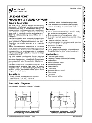
  • 1. LM2907/LM2917 Frequency to Voltage Converter December 9, 2008 LM2907/LM2917 Frequency to Voltage Converter General Description ■ Only one RC network provides frequency doubling ■ Zener regulator on chip allows accurate and stable The LM2907, LM2917 series are monolithic frequency to volt- frequency to voltage or current conversion (LM2917) age converters with a high gain op amp/comparator designed to operate a relay, lamp, or other load when the input fre- quency reaches or exceeds a selected rate. The tachometer Features uses a charge pump technique and offers frequency doubling ■ Ground referenced tachometer input interfaces directly for low ripple, full input protection in two versions (LM2907-8, with variable reluctance magnetic pickups LM2917-8) and its output swings to ground for a zero fre- ■ Op amp/comparator has floating transistor output quency input. ■ 50 mA sink or source to operate relays, solenoids, meters, The op amp/comparator is fully compatible with the tachome- or LEDs ter and has a floating transistor as its output. This feature ■ Frequency doubling for low ripple allows either a ground or supply referred load of up to 50 mA. The collector may be taken above VCC up to a maximum ■ Tachometer has built-in hysteresis with either differential input or ground referenced input VCE of 28V. ■ Built-in zener on LM2917 The two basic configurations offered include an 8-pin device with a ground referenced tachometer input and an internal ■ ±0.3% linearity typical connection between the tachometer output and the op amp ■ Ground referenced tachometer is fully protected from non-inverting input. This version is well suited for single speed damage due to swings above VCC and below ground or frequency switching or fully buffered frequency to voltage conversion applications. Applications The more versatile configurations provide differential ■ Over/under speed sensing tachometer input and uncommitted op amp inputs. With this version the tachometer input may be floated and the op amp ■ Frequency to voltage conversion (tachometer) becomes suitable for active filter conditioning of the tachome- ■ Speedometers ter output. ■ Breaker point dwell meters Both of these configurations are available with an active shunt ■ Hand-held tachometer regulator connected across the power leads. The regulator ■ Speed governors clamps the supply such that stable frequency to voltage and ■ Cruise control frequency to current operations are possible with any supply voltage and a suitable resistor. ■ Automotive door lock control ■ Clutch control Advantages ■ Horn control ■ Output swings to ground for zero frequency input ■ Touch or sound switches ■ Easy to use; VOUT = fIN × VCC × R1 × C1 Connection Diagrams Dual-In-Line and Small Outline Packages, Top Views 794201 794202 Order Number LM2907M-8 or LM2907N-8 Order Number LM2917M-8 or LM2917N-8 See NS Package Number M08A or N08E See NS Package Number M08A or N08E © 2008 National Semiconductor Corporation 7942 www.national.com
  • 2. LM2907/LM2917 794203 794204 Order Number LM2907M or LM2907N Order Number LM2917M or LM2917N See NS Package Number M14A or N14A See NS Package Number M14A or N14A Ordering Information Order Package Package Package Supplied Number Type Number Marking As LM2907M-8 8-Pin SOIC Narrow M08A LM2907M-8 Rail of 95 LM2907MX-8 8-Pin SOIC Narrow M08A LM2907M-8 Reel of 2500 LM2907M 14-Pin SOIC Narrow M14A LM2907M Rail of 55 LM2907MX 14-Pin SOIC Narrow M14A LM2907M Reel of 2500 LM2907N-8 8-Pin Molded DIP N08E LM2907N-8 Rail of 40 LM2907N 14-Pin Molded DIP N14A LM2907N Rail of 25 LM2917M-8 8-Pin SOIC Narrow M08A LM2917M-8 Rail of 95 LM2917MX-8 8-Pin SOIC Narrow M08A LM2917M-8 Reel of 2500 LM2917M 14-Pin SOIC Narrow M14A LM2917M Rail of 55 LM2917MX 14-Pin SOIC Narrow M14A LM2917M Reel of 2500 LM2917N-8 8-Pin Molded DIP N08E LM2917N-8 Rail of 40 LM2917N 14-Pin Molded DIP N14A LM2917N Rail of 25 www.national.com 2
  • 3. LM2907/LM2917 Absolute Maximum Ratings (Note 1) Op Amp/Comparator 0.0V to +28V Power Dissipation If Military/Aerospace specified devices are required, please contact the National Semiconductor Sales Office/ LM2907-8, LM2917-8 1200 mW Distributors for availability and specifications. LM2907-14, LM2917-14 1580 mW See (Note 1) Supply Voltage 28V Operating Temperature Range −40°C to +85°C Supply Current (Zener Options) 25 mA Storage Temperature Range −65°C to +150°C Collector Voltage 28V Soldering Information Differential Input Voltage Dual-In-Line Package Tachometer 28V Soldering (10 seconds) 260°C Op Amp/Comparator 28V Small Outline Package Input Voltage Range Vapor Phase (60 seconds) 215°C Tachometer Infrared (15 seconds) 220°C LM2907-8, LM2917-8 ±28V LM2907, LM2917 0.0V to +28V Electrical Characteristics VCC = 12 VDC, TA = 25°C, see test circuit Symbol Parameter Conditions Min Typ Max Units TACHOMETER Input Thresholds VIN = 250 mVp-p @ 1 kHz (Note 2) ±10 ±25 ±40 mV Hysteresis VIN = 250 mVp-p @ 1 kHz (Note 2) 30 mV Offset Voltage VIN = 250 mVp-p @ 1 kHz (Note 2) LM2907/LM2917 3.5 10 mV LM2907-8/LM2917-8 5 15 mV Input Bias Current VIN = ±50 mVDC 0.1 1 μA VOH Pin 2 VIN = +125 mVDC (Note 3) 8.3 V VOL Pin 2 VIN = −125 mVDC (Note 3) 2.3 V I2, I3 Output Current V2 = V3 = 6.0V (Note 4) 140 180 240 μA I3 Leakage Current I2 = 0, V3 = 0 0.1 μA K Gain Constant (Note 3) 0.9 1.0 1.1 Linearity fIN = 1 kHz, 5 kHz, 10 kHz (Note 5) −1.0 0.3 +1.0 % OP/AMP COMPARATOR VOS VIN = 6.0V 3 10 mV IBIAS VIN = 6.0V 50 500 nA Input Common-Mode Voltage 0 VCC−1.5V V Voltage Gain 200 V/mV Output Sink Current VC = 1.0 40 50 mA Output Source Current VE = VCC −2.0 10 mA Saturation Voltage ISINK = 5 mA 0.1 0.5 V ISINK = 20 mA 1.0 V ISINK = 50 mA 1.0 1.5 V ZENER REGULATOR Regulator Voltage RDROP = 470Ω 7.56 V Series Resistance 10.5 15 Ω Temperature Stability +1 mV/°C Total Supply Current 3.8 6 mA Note 1: For operation in ambient temperatures above 25°C, the device must be derated based on a 150°C maximum junction temperature and a thermal resistance of 101°C/W junction to ambient for LM2907-8 and LM2917-8, and 79°C/W junction to ambient for LM2907-14 and LM2917-14. Note 2: Hysteresis is the sum +VTH − (−VTH), offset voltage is their difference. See test circuit. Note 3: VOH is equal to ¾ × VCC − 1 VBE, VOL is equal to ¼ × VCC − 1 VBE therefore VOH − VOL = VCC/2. The difference, VOH − VOL, and the mirror gain, I2/I3, are the two factors that cause the tachometer gain constant to vary from 1.0. Note 4: Be sure when choosing the time constant R1 × C1 that R1 is such that the maximum anticipated output voltage at pin 3 can be reached with I3 × R1. The maximum value for R1 is limited by the output resistance of pin 3 which is greater than 10 MΩ typically. 3 www.national.com
  • 4. LM2907/LM2917 Note 5: Nonlinearity is defined as the deviation of VOUT (@ pin 3) for fIN = 5 kHz from a straight line defined by the VOUT @ 1 kHz and VOUT @ 10 kHz. C1 = 1000 pF, R1 = 68k and C2 = 0.22 mFd. Test Circuit and Waveform 794206 Tachometer Input Threshold Measurement 794207 www.national.com 4
  • 5. LM2907/LM2917 Typical Performance Characteristics Tachometer Linearity Tachometer Linearity vs Temperature vs Temperature 794246 794247 Total Supply Current Zener Voltage vs Temperature 794240 794241 Normalized Tachometer Output (K) Normalized Tachometer Output (K) vs Temperature vs Temperature 794242 794243 5 www.national.com
  • 6. LM2907/LM2917 Tachometer Currents I2and I3 Tachometer Currents I2and I3 vs Supply Voltage vs Temperature 794244 794245 Tachometer Linearity vs R1 Tachometer Input Hysteresis vs Temperature 794248 794249 Op Amp Output Transistor Op Amp Output Transistor Characteristics Characteristics 794251 794250 www.national.com 6
  • 7. LM2907/LM2917 The size of C2 is dependent only on the amount of ripple volt- Applications Information age allowable and the required response time. The LM2907 series of tachometer circuits is designed for minimum external part count applications and maximum ver- CHOOSING R1 AND C1 satility. In order to fully exploit its features and advantages There are some limitations on the choice of R1 and C1 which let's examine its theory of operation. The first stage of oper- should be considered for optimum performance. The timing ation is a differential amplifier driving a positive feedback flip- capacitor also provides internal compensation for the charge flop circuit. The input threshold voltage is the amount of pump and should be kept larger than 500 pF for very accurate differential input voltage at which the output of this stage operation. Smaller values can cause an error current on R1, changes state. Two options (LM2907-8, LM2917-8) have one especially at low temperatures. Several considerations must input internally grounded so that an input signal must swing be met when choosing R1. The output current at pin 3 is in- above and below ground and exceed the input thresholds to ternally fixed and therefore VO/R1 must be less than or equal produce an output. This is offered specifically for magnetic to this value. If R1 is too large, it can become a significant variable reluctance pickups which typically provide a single- fraction of the output impedance at pin 3 which degrades lin- ended ac output. This single input is also fully protected earity. Also output ripple voltage must be considered and the against voltage swings to ±28V, which are easily attained with size of C2 is affected by R1. An expression that describes the these types of pickups. ripple content on pin 3 for a single R1C2 combination is: The differential input options (LM2907, LM2917) give the user the option of setting his own input switching level and still have the hysteresis around that level for excellent noise rejection in any application. Of course in order to allow the inputs to attain common-mode voltages above ground, input protection is removed and neither input should be taken outside the lim- It appears R1 can be chosen independent of ripple, however its of the supply voltage being used. It is very important that response time, or the time it takes VOUT to stabilize at a new an input not go below ground without some resistance in its voltage increases as the size of C2 increases, so a compro- lead to limit the current that will then flow in the epi-substrate mise between ripple, response time, and linearity must be diode. chosen carefully. Following the input stage is the charge pump where the input As a final consideration, the maximum attainable input fre- frequency is converted to a dc voltage. To do this requires quency is determined by VCC, C1 and I2: one timing capacitor, one output resistor, and an integrating or filter capacitor. When the input stage changes state (due to a suitable zero crossing or differential voltage on the input) the timing capacitor is either charged or discharged linearly between two voltages whose difference is VCC/2. Then in one USING ZENER REGULATED OPTIONS (LM2917) half cycle of the input frequency or a time equal to 1/2 fIN the change in charge on the timing capacitor is equal to VCC/2 × For those applications where an output voltage or current C1. The average amount of current pumped into or out of the must be obtained independent of supply voltage variations, capacitor then is: the LM2917 is offered. The most important consideration in choosing a dropping resistor from the unregulated supply to the device is that the tachometer and op amp circuitry alone require about 3 mA at the voltage level provided by the zener. At low supply voltages there must be some current flowing in the resistor above the 3 mA circuit current to operate the reg- The output circuit mirrors this current very accurately into the ulator. As an example, if the raw supply varies from 9V to 16V, load resistor R1, connected to ground, such that if the pulses a resistance of 470Ω will minimize the zener voltage variation of current are integrated with a filter capacitor, then VO = ic × to 160 mV. If the resistance goes under 400Ω or over 600Ω R1, and the total conversion equation becomes: the zener variation quickly rises above 200 mV for the same VO = VCC × fIN × C1 × R1 × K input variation. Where K is the gain constant—typically 1.0. 7 www.national.com
  • 8. LM2907/LM2917 Typical Applications Minimum Component Tachometer 794208 ”Speed Switch”, Load is Energized when fIN ≥ (1 / ( 2RC)) 794209 www.national.com 8
  • 9. LM2907/LM2917 Zener Regulated Frequency to Voltage Converter 794210 Breaker Point Dwell Meter 794211 9 www.national.com
  • 10. LM2907/LM2917 Voltage Driven Meter Indicating Engine RPM VO = 6V @ 400 Hz or 6000 ERPM (8 Cylinder Engine) 794212 Current Driven Meter Indicating Engine RPM IO = 10 mA @ 300 Hz or 6000 ERPM (6 Cylinder Engine) 794213 www.national.com 10
  • 11. LM2907/LM2917 Capacitance Meter VOUT = 1V–10V for CX = 0.01 to 0.1 mFd (R = 111k) 794214 Two-Wire Remote Speed Switch 794215 11 www.national.com
  • 12. LM2907/LM2917 100 Cycle Delay Switch 794216 Variable Reluctance Magnetic Pickup Buffer Circuits 794239 794217 Precision two-shot output frequency equals twice input frequency. Pulse height = VZENER www.national.com 12
  • 13. LM2907/LM2917 Finger Touch or Contact Switch 794219 794218 Flashing LED Indicates Overspeed 794220 Flashing begins when fIN ≥ 100 Hz. Flash rate increases with input frequency increase beyond trip point. 13 www.national.com
  • 14. LM2907/LM2917 Frequency to Voltage Converter with 2 Pole Butterworth Filter to Reduce Ripple 794221 Overspeed Latch 794223 794222 www.national.com 14
  • 15. LM2907/LM2917 Some Frequency Switch Applications May Require Hysteresis in the Comparator Function Which can be Implemented in Several Ways 794224 794225 794226 794227 794228 15 www.national.com
  • 16. LM2907/LM2917 Changing the Output Voltage for an Input Frequency of Zero 794230 794229 Changing Tachometer Gain Curve or Clamping the Minimum Output Voltage 794232 794231 www.national.com 16
  • 17. LM2907/LM2917 Anti-Skid Circuit Functions “Select-Low” Circuit 794234 VOUT is proportional to the lower of the two input wheel speeds. 794233 “Select-High” Circuit 794236 VOUT is proportional to the higher of the two input wheel speeds. 794235 “Select-Average” Circuit 794237 17 www.national.com
  • 18. LM2907/LM2917 www.national.com Equivalent Schematic Diagram 18 794238 *This connection made on LM2907-8 and LM2917-8 only. **This connection made on LM2917 and LM2917-8 only.
  • 19. LM2907/LM2917 Physical Dimensions inches (millimeters) unless otherwise noted 8-Lead (0.150″ Wide) Molded Small Outline Package, JEDEC Order Number LM2907M-8 or LM2917M-8 NS Package Number M08A 19 www.national.com
  • 20. LM2907/LM2917 Molded SO Package (M) Order Number LM2907M or LM2917M NS Package Number M14A Molded Dual-In-Line Package (N) Order Number LM2907N-8 or LM2917N-8 NS Package Number N08E www.national.com 20
  • 21. LM2907/LM2917 Molded Dual-In-Line Package (N) Order Number LM2907N or LM2917N NS Package Number N14A 21 www.national.com
  • 22. LM2907/LM2917 Frequency to Voltage Converter Notes For more National Semiconductor product information and proven design tools, visit the following Web sites at: Products Design Support Amplifiers www.national.com/amplifiers WEBENCH® Tools www.national.com/webench Audio www.national.com/audio App Notes www.national.com/appnotes Clock and Timing www.national.com/timing Reference Designs www.national.com/refdesigns Data Converters www.national.com/adc Samples www.national.com/samples Interface www.national.com/interface Eval Boards www.national.com/evalboards LVDS www.national.com/lvds Packaging www.national.com/packaging Power Management www.national.com/power Green Compliance www.national.com/quality/green Switching Regulators www.national.com/switchers Distributors www.national.com/contacts LDOs www.national.com/ldo Quality and Reliability www.national.com/quality LED Lighting www.national.com/led Feedback/Support www.national.com/feedback Voltage Reference www.national.com/vref Design Made Easy www.national.com/easy PowerWise® Solutions www.national.com/powerwise Solutions www.national.com/solutions Serial Digital Interface (SDI) www.national.com/sdi Mil/Aero www.national.com/milaero Temperature Sensors www.national.com/tempsensors Solar Magic® www.national.com/solarmagic Wireless (PLL/VCO) www.national.com/wireless Analog University® www.national.com/AU THE CONTENTS OF THIS DOCUMENT ARE PROVIDED IN CONNECTION WITH NATIONAL SEMICONDUCTOR CORPORATION (“NATIONAL”) PRODUCTS. NATIONAL MAKES NO REPRESENTATIONS OR WARRANTIES WITH RESPECT TO THE ACCURACY OR COMPLETENESS OF THE CONTENTS OF THIS PUBLICATION AND RESERVES THE RIGHT TO MAKE CHANGES TO SPECIFICATIONS AND PRODUCT DESCRIPTIONS AT ANY TIME WITHOUT NOTICE. NO LICENSE, WHETHER EXPRESS, IMPLIED, ARISING BY ESTOPPEL OR OTHERWISE, TO ANY INTELLECTUAL PROPERTY RIGHTS IS GRANTED BY THIS DOCUMENT. TESTING AND OTHER QUALITY CONTROLS ARE USED TO THE EXTENT NATIONAL DEEMS NECESSARY TO SUPPORT NATIONAL’S PRODUCT WARRANTY. EXCEPT WHERE MANDATED BY GOVERNMENT REQUIREMENTS, TESTING OF ALL PARAMETERS OF EACH PRODUCT IS NOT NECESSARILY PERFORMED. NATIONAL ASSUMES NO LIABILITY FOR APPLICATIONS ASSISTANCE OR BUYER PRODUCT DESIGN. BUYERS ARE RESPONSIBLE FOR THEIR PRODUCTS AND APPLICATIONS USING NATIONAL COMPONENTS. PRIOR TO USING OR DISTRIBUTING ANY PRODUCTS THAT INCLUDE NATIONAL COMPONENTS, BUYERS SHOULD PROVIDE ADEQUATE DESIGN, TESTING AND OPERATING SAFEGUARDS. EXCEPT AS PROVIDED IN NATIONAL’S TERMS AND CONDITIONS OF SALE FOR SUCH PRODUCTS, NATIONAL ASSUMES NO LIABILITY WHATSOEVER, AND NATIONAL DISCLAIMS ANY EXPRESS OR IMPLIED WARRANTY RELATING TO THE SALE AND/OR USE OF NATIONAL PRODUCTS INCLUDING LIABILITY OR WARRANTIES RELATING TO FITNESS FOR A PARTICULAR PURPOSE, MERCHANTABILITY, OR INFRINGEMENT OF ANY PATENT, COPYRIGHT OR OTHER INTELLECTUAL PROPERTY RIGHT. LIFE SUPPORT POLICY NATIONAL’S PRODUCTS ARE NOT AUTHORIZED FOR USE AS CRITICAL COMPONENTS IN LIFE SUPPORT DEVICES OR SYSTEMS WITHOUT THE EXPRESS PRIOR WRITTEN APPROVAL OF THE CHIEF EXECUTIVE OFFICER AND GENERAL COUNSEL OF NATIONAL SEMICONDUCTOR CORPORATION. As used herein: Life support devices or systems are devices which (a) are intended for surgical implant into the body, or (b) support or sustain life and whose failure to perform when properly used in accordance with instructions for use provided in the labeling can be reasonably expected to result in a significant injury to the user. A critical component is any component in a life support device or system whose failure to perform can be reasonably expected to cause the failure of the life support device or system or to affect its safety or effectiveness. National Semiconductor and the National Semiconductor logo are registered trademarks of National Semiconductor Corporation. All other brand or product names may be trademarks or registered trademarks of their respective holders. Copyright© 2008 National Semiconductor Corporation For the most current product information visit us at www.national.com National Semiconductor National Semiconductor Europe National Semiconductor Asia National Semiconductor Japan Americas Technical Technical Support Center Pacific Technical Support Center Technical Support Center Support Center Email: europe.support@nsc.com Email: ap.support@nsc.com Email: jpn.feedback@nsc.com Email: support@nsc.com German Tel: +49 (0) 180 5010 771 Tel: 1-800-272-9959 English Tel: +44 (0) 870 850 4288 www.national.com