![M E T R O L O G Y
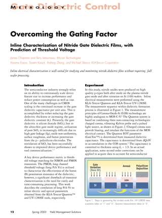
The experiment is designed to have the
Corona Bias, Kelvin Probe, Surface Photovoltage, nitridation process as the major excur-
Q VSurf SPV sion mode for the purpose of evaluating
+8kV LIGHT
Mechanical
Oscillator
this concept. The Pchannel Vt is chosen
Corona
Source, Kelvin Probe
Electronics
Transient
Detection
as the end of line monitor due to its
CO3-, H30+ sensitivity to B penetration resulting
SPV
VSurf
OXIDE from the poly doping and source/drain
P SILICON formation steps. The long Pchannel
transistor is chosen because the Vt is
1. 2. 3. primary controlled by the gate, unlike
Apply Q Corona Bias Measure V S (=V OX + ψ) Stop vibration, flash light, the short channel device, where the turn
Measure each ∆ Q Probe vibration drives and measure SPV
AC current: dψ
on characteristics are heavy influenced
I ≈C dt by the drain voltage (phenomena known
I = V S - V kp
dC as drain induced barrier lowering10).
dt This concept is illustrated in Figure 3.
4. Repeat
The inline characterization parameters
are affected by the physical thickness,
Figure 2. Quantox COS measurement theor y.
composition, and quality (or leakage) of
the film. Table 1 highlights the impact of film charac-
band-bending. The tunneling voltage (Vtunnel) parameter teristics that result in a positive shift in the Vt, and the
is used to monitor the high-field leakage properties of corresponding response of the inline parameters. The
the oxide. All dielectrics eventually reach a point where, physical interpretations of these parameters are easily
as more and more charge is applied, the voltage across related to physical thickness, dielectric quality (or
the dielectric reaches the maximum sustainable volt- resistance to gate leakage) and nitrogen content.
age, defined as Vtunnel. Vtunnel provides a good indication
of the oxide integrity and quality in a manner similar The predicted Vt is a model built on linear combinations
to more traditional soft-breakdown measurements. of inline parameters. This approach (the model) uses a
order Taylor Series expansion of the functional responses
The inline electrical measurements were done on moni- of Vt to the inline parameters. The model is developed
tor wafers, with one wafer per lot, five sites per wafer. using SAS JMP4 software and has the form of
The end of line electrical data comes from two to twelve
probed wafers per lot, nine sites per wafer. The lot aver- Y = ax1 + bx2 + cx3 ...
ages are used for correlation in this study.
where Y is Vt; a, b, c are coefficients; and x1, x2, and x3
are inline parameters. The fit of the predicted data to the
Results and discussion
The equation for threshold voltage is provided in
Equation 1.10 The major contributions to the Vt are
Poly Poly
film capacitance (Cox), bulk Si band bending (YB) and
substrate doping (NA). The later two (YB and NA) are Gate Gate
controlled primarily by near surface doping of channel.
The inline measurements are not sensitive to variations
in surface doping of channel due to absence of any Vt
adjusted doping on inline samples. Si Substrate
Si Substrate
Long Channel Short Channel
[
Vt = öms –
Qeff
Cox ]
+ 2ΨB
Gate Controlled Drain Controlled
√4åsiqNAΨB
+ Figure 3. Schematic highlighting the requirement of monitoring long
Cox
Pchannel devices for B penetration resistance. Variations in nitridation
Equation 1. Textbook calculation of Vt for MOS transistor, from SZE 10 .
will impact the degree of B penetration resistance.
Spring 2003 Yield Management Solutions 13](data:image/gif;base64,R0lGODlhAQABAIAAAAAAAP///yH5BAEAAAAALAAAAAABAAEAAAIBRAA7)
Empfohlen
Empfohlen
Weitere ähnliche Inhalte
Kürzlich hochgeladen
Kürzlich hochgeladen (20)
Empfohlen
Empfohlen (20)
Overcoming Gating Factor
- 1. Gate Dielectric Control M E T R O L O G Y Overcoming the Gating Factor Inline Characterization of Nitride Gate Dielectric Films, with Prediction of Threshold Voltage James Chapman and Terry Letourneau, Micron Technologies Kwame Eason, Torsten Kaack, Xiafang Zhang, and Michael Slessor, KLA-Tencor Corporation Inline electrical characterization is well-suited for studying and monitoring nitride dielectric films without requiring full wafer processing. Introduction Experiment The semiconductor industry strongly relies In this study, nitride oxides were produced on high on its ability to continuously scale device quality p-types both after oxide on the plasma nitride feature size to increase performance and gate oxide and after nitration on Si (100) wafers. Inline reduce power consumption as well as cost. electrical measurements were performed using the One of the many challenges in CMOS KLA-Tencor Quantox and KLA-Tencor UV-1280SE. scaling is the continued increase in the gate The measurement sequence within dielectric formation dielectric capacitance per unit area. This is process is illustrated in Figure 1. The measurement accomplished by either reducing the gate principles of Corona-Oxide-Si (COS) technology are dielectric thickness or increasing the gate highly analogous to MOS C-V.8 The Quantox system is dielectric constant (εr). Presently, the gate based on combining three non-contacting technologies: dielectric is silicon dioxide (SiO2), but in charged corona, vibrating Kelvin probe and a pulsed the ultra-thin gate oxide regime, utilization light source, as shown in Figure 2. Charged corona ions of pure SiO2 is increasingly difficult due to provide biasing, and emulate the functions of the MOS high gate leakage (Ig), oxide non-uniformity, electrical contact. The Quantox EOT parameter surface roughness, and boron penetration (GateTox™) is determined from measured dielectric from the p+ polysilicon electrodes. The capacitance. The capacitance is determined from dQ/dV nitridation of SiO2 has been successfully in accumulation in the COS system.9 The capacitance is shown to improved device performance and converted to thickness using εr = 3.9. In an actual tool commercialization.1-7 application, some second order corrections can be applied to acquire data to account for semiconductor A key device performance metric is thresh- old voltage matching for NMOS and PMOS transistors. The PMOS, long channel Gate Anneal Polysilicon threshold voltage (long Pch Vt) is utilized Oxidation Deposition to characterize the effectiveness of the boron (Base OX) (B) penetration resistance of the dielectric; however, a significant drawback of transistor characterization is the need for costly and SiON time-consuming processing. This work Si Si describes the correlation of long Pch Vt to 1 2 3 inline electric and optical parameters obtained from the KLA-Tencor Quantox™ and UV-1280SE tools, respectively. Figure 1. Steps in generating the nitrided oxide film. UV-1280SE mea- surements taken at “1” and “3”, Quantox measurements taken at “3”. 12 1 Spring 2003 Yield Management Solutions
- 2. M E T R O L O G Y The experiment is designed to have the Corona Bias, Kelvin Probe, Surface Photovoltage, nitridation process as the major excur- Q VSurf SPV sion mode for the purpose of evaluating +8kV LIGHT Mechanical Oscillator this concept. The Pchannel Vt is chosen Corona Source, Kelvin Probe Electronics Transient Detection as the end of line monitor due to its CO3-, H30+ sensitivity to B penetration resulting SPV VSurf OXIDE from the poly doping and source/drain P SILICON formation steps. The long Pchannel transistor is chosen because the Vt is 1. 2. 3. primary controlled by the gate, unlike Apply Q Corona Bias Measure V S (=V OX + ψ) Stop vibration, flash light, the short channel device, where the turn Measure each ∆ Q Probe vibration drives and measure SPV AC current: dψ on characteristics are heavy influenced I ≈C dt by the drain voltage (phenomena known I = V S - V kp dC as drain induced barrier lowering10). dt This concept is illustrated in Figure 3. 4. Repeat The inline characterization parameters are affected by the physical thickness, Figure 2. Quantox COS measurement theor y. composition, and quality (or leakage) of the film. Table 1 highlights the impact of film charac- band-bending. The tunneling voltage (Vtunnel) parameter teristics that result in a positive shift in the Vt, and the is used to monitor the high-field leakage properties of corresponding response of the inline parameters. The the oxide. All dielectrics eventually reach a point where, physical interpretations of these parameters are easily as more and more charge is applied, the voltage across related to physical thickness, dielectric quality (or the dielectric reaches the maximum sustainable volt- resistance to gate leakage) and nitrogen content. age, defined as Vtunnel. Vtunnel provides a good indication of the oxide integrity and quality in a manner similar The predicted Vt is a model built on linear combinations to more traditional soft-breakdown measurements. of inline parameters. This approach (the model) uses a order Taylor Series expansion of the functional responses The inline electrical measurements were done on moni- of Vt to the inline parameters. The model is developed tor wafers, with one wafer per lot, five sites per wafer. using SAS JMP4 software and has the form of The end of line electrical data comes from two to twelve probed wafers per lot, nine sites per wafer. The lot aver- Y = ax1 + bx2 + cx3 ... ages are used for correlation in this study. where Y is Vt; a, b, c are coefficients; and x1, x2, and x3 are inline parameters. The fit of the predicted data to the Results and discussion The equation for threshold voltage is provided in Equation 1.10 The major contributions to the Vt are Poly Poly film capacitance (Cox), bulk Si band bending (YB) and substrate doping (NA). The later two (YB and NA) are Gate Gate controlled primarily by near surface doping of channel. The inline measurements are not sensitive to variations in surface doping of channel due to absence of any Vt adjusted doping on inline samples. Si Substrate Si Substrate Long Channel Short Channel [ Vt = öms – Qeff Cox ] + 2ΨB Gate Controlled Drain Controlled √4åsiqNAΨB + Figure 3. Schematic highlighting the requirement of monitoring long Cox Pchannel devices for B penetration resistance. Variations in nitridation Equation 1. Textbook calculation of Vt for MOS transistor, from SZE 10 . will impact the degree of B penetration resistance. Spring 2003 Yield Management Solutions 13
- 3. M E T R O L O G Y Causes for Physical Dielectric Nitrogen models range in total inline parameters, the least being PMOS V1 to Thickness Quality Content two and the most being six (i.e. the model is based on increase (↑) (↑) (↑) two to six inline parameters). GateTox (EOT) ↑ ↓ Device -Vtunnel ↑ ↑ ↓ Model 1 2 3 ρox ↑ ↑ Optimize 1 0.988 0.795 0.839 Dit ↑ Adjust R2 0.971 0.549 0.645 Reflectivity ↓ ↓ Optimize 2 0.952 0.986 0.976 Adjust R2 0.875 0.970 0.948 Table 1. Parameter response table variations in gate dielectric result- General Function 0.952 0.986 0.976 ing in a PMOS V t increase. Adjust R2 0.875 0.970 0.948 Table 2. Table highlighting the optimization V t models for different actual data is presented in Figure 4. The model is devices. (Note that a “General Function” is a metric which has reasonably based on 12 observations, which is the lower end of good application to all devices). The general function has the same establishing a statistical population. The methodology is parameters but different coefficients from device to device. applied to three devices, each with varying base oxides and transistor process flows. A “super-set” of parameters Conclusions Actual by Predicted Plot In this paper, nitrided oxide films have been character- -0.5 ized using inline non-contact electrical and optical Vt, S91 (0058 Actual 0.55 measurements. The correlation obtained between the -0.6 EoL Long Pchannel Vt actual and predicted (based on -0.65 inline parameters) has resulted in R2 > 0.97 for indi- -0.7 vidually optimized models. The individually optimized -0.75 models incorporate ~6 inline parameters. A two para- -0.8 -0.7 -0.6 -0.5 -0.4 Vt, Predicted P=0.0002 meter model has been successfully developed for one RSq=0.99 RMSE=0.0104 device with R2 > 0.90 and adjusted R2 > 0.88. These Summary of Fit results support that the inline monitoring is sensitive RSquare 0.986438 RSquare Adj 0.970163 to process variations that impact end of line measure- Root Mean Square Error 0.01045 Mean of Response -0.61093 ments, when nitridation is the primary excursion mode. Observations (or Sum Wgts) 12 The correlation obtained between Long Pchannel Vt and Summary of Fit Source DF Sum of Squares Mean Square F Ratio model-based Quantox and UV-1280SE measurements Model 6 0.03971326 0.006619 60.6119 Error 5 0.00054600 0.000109 Prob>F demonstrates that inline electrical characterization is C. Total 11 0.04025926 0.0002 well suited for studying and monitoring nitrided dielectric films without requiring full wafer processing. Figure 4. Predicted versus Actual V t for one device. The R 2 fit is > 0.98 and adjusted R 2 > 0.97, with 12 observations. References 1. S. Hattangady et al., SPIE Symp. Microelec. Manf. have been determined for application to all data sets. (1998). The criteria for successful model generation is R2 > 2. D.T. Grider, et al. VLSI 1997, p. 47-8. (1997). 0.9, with adjusted R2 > 0.85. Table 2 highlights the 3. Rodder-M, et al., IEDM 1998, p. 623-6. (1998). application of the “general” functional model to all 4. K. Eason et al., 198th ECS Toronto, p195-203 (2000). three data sets. The application of this model means 5. F. Cubaynes. IEEE ASMC 2002, TBP. that the inline parameters comprising the model are 6. K. Eason et al., AVS ICMI, p251-3 (2002). constant; however, the coefficients in the models are dif- 7. H.N. Al-Shareef, et al., 198th ECS Toronto, p210-213 ferent for the various devices. The general model func- (2000). tional form is provided in Equation 2. The optimized 8. J. Guan et al., ECS, MA 99-2 p1106 (1999). 9. T. G. Miller, Semi. International, July (1995). 10. S. M. Sze, Semiconductor Devices Physics and VT = f(SPV,Dit,Tox,∆Ref,Vtun,ρox,Qtotal) Technology, 1985. Equation 2. Super-set of parameters used in optimized model. The “General Function” uses six parameters. 14 Spring 2003 Yield Management Solutions
- 4. Upset over 90 nm gate stack control? Quantox XP Inline, independent electrical Take two and accelerate yield as needed. measurement of gate leak- age and capacitance, and It’s time to alleviate the pain of gate stack control. Because with gate dielectrics correlation to end of line growing more complex and measuring less than 20 Å, you’re bound to experience transistor parametric tests. problems with film thickness variations, composition, capacitance and leakage. So SpectraFx 100 Ultra what’s the remedy? It’s a combination of optical metrology to control thickness precise, reliable optical and composition, and electrical metrology to control capacitance and leakage. monitoring of extremely And only KLA-Tencor has both. Giving you better gate stack control. While speeding thin gate dielectrics on your way to higher yields at 90 nm. Now that’s relief. product wafers. For solutions and strategies for gate stack control, please visit us at www.kla-tencor.com/GateXpress Accelerating Yield ©2002 KLA-Tencor Corporation