SlideShare ist ein Scribd-Unternehmen logo
1 von 14
Downloaden Sie, um offline zu lesen
Class A Amplifier
Common emitter voltage amplifiers are the most commonly used type of amplifier as they have a large
voltage gain. They are designed to produce a large output voltage swing from a relatively small input
signal voltage of only a few millivolt's and are used mainly as "Small Signal Amplifiers" as we saw in the
previous tutorials. However, sometimes an amplifier is required to drive large resistive loads such as a
loudspeaker and for these types of applications where high switching currents are needed Power
Amplifiers are required.
The main function of the Power amplifier, which are also known as a "Large Signal Amplifier" is to deliver
power, which is the product of voltage and current to the load. Basically a power amplifier is also a
voltage amplifier the difference being that the load resistance connected to the output is relatively low, for
example a loudspeaker of 4 or 8Ωs resulting in high currents flowing through the Collector of the
transistor. Because of these high load currents the output transistor(s) used for power amplifier output
stages need to have higher voltage and power ratings than the general ones used for small signal stages.
Since we are interested in delivering maximum AC power to the load, while consuming the minimum DC
power possible from the supply we are mostly concerned with the "Conversion Efficiency" of the amplifier.
However, one of the main disadvantage of power amplifiers and especially Class A type amplifiers is that
their overall conversion efficiency is very low. Percentage efficiency in amplifiers is defined as the r.m.s.
output power dissipated in the load divided by the total DC power taken from the supply source as shown
below.
Power Amplifier Efficiency


    ď‚·             Where:
    ď‚·
                 η% - is the efficiency of the amplifier.
    ď‚·
    ď‚·             Pout - is the amplifiers output power delivered to the load.
    ď‚·
    ď‚·             Pdc - is the DC power taken from the supply.
For a power amplifier it is very important that the amplifiers power supply is well designed to provide the
maximum available continuous power to the output signal.
Class A Amplifier
The most commonly used type of power amplifier configuration is the Class A Amplifier. Class A
amplifier stages use the transistor in the standard Common Emitter circuit configuration as seen
previously, in which the transistor is always biased "ON" so that it conducts during one complete cycle of
the input signal waveform producing minimum distortion to the output. This means then that the Class A
Amplifierconfiguration is the ideal operating mode, because there can be no crossover or switch-off
distortion to the output waveform. Class A power amplifier output stages may use a single transistor or
pairs of transistors connected together to share the high load current. Consider the Class A
amplifier circuit below.
Single-ended Amplifier Circuit


This is the simplest type of Class A power amplifier circuit. It uses a single-ended transistor for its output
stage with the resistive load connected directly to the Collector terminal. When the transistor switches
"ON" it sinks the output current through the Collector resulting in an inevitable voltage drop across the
Emitter resistance thereby limiting the negative output capability. The efficiency of this type of circuit is
very low (possibly 20%) and delivers small power outputs for a large drain on the DC power supply. A
Class A amplifier stage passes the same load current even when no input signal is applied so large
heatsinks are needed for the output transistors.
However, another simple way to increase the current handling capacity of the circuit while at the same
time obtain a greater power gain is to replace the single output transistor with a Darlington Transistor.
These types of devices are basically two transistors within a single package, one small "pilot" transistor
and another larger "switching" transistor. The big advantage of these devices are that the input
impedance is suitably large while the output impedance is relatively low, thereby reducing the power loss
and therefore the heat within the switching device.
Darlington Transistor Configurations
The overall current gain Beta (β) or Hfe value of a Darlington device is the product of the two individual
gains of the transistors multiplied together and very high β values along with high Collector currents are
possible compared to a single transistor circuit.
To improve the full power efficiency of the Class A amplifier it is possible to design the circuit with a
transformer connected directly in the Collector circuit to form a circuit called a Transformer Coupled
Amplifier. This improves the efficiency of the amplifier by matching the impedance of the load with that of
the amplifiers output using the turns ratio (N) of the transformer and an example is given below.
Transformer-coupled Amplifier Circuit


As the Collector current, Ic is reduced to below the quiescent Q-point set up by the Base bias voltage,
due to variations in the Base current, the magnetic flux in the transformer core collapses causing an
induced emf in the transformer primary windings. This causes an instantaneous Collector voltage to rise
to a value of twice the supply voltage 2Vcc giving a maximum Collector current of twice Ic when the
Collector voltage is at its minimum. Then the efficiency of this type of Class A amplifier configuration can
be calculated as follows.
The r.m.s. Collector voltage is given as:


The r.m.s. Collector current is given as:


The r.m.s. Power delivered to the load (Pac) is therefore given as:


The average power drawn from the supply (Pdc) is given by:


and therefore the efficiency of a Transformer-coupled Class A amplifier is given as:


This improves the efficiency of the amplifier by matching the impedance of the load with that of the
amplifier using the turns ratio of the transformer and efficiencies reaching 40% are possible with most
commercially available Class-A type power amplifiers of this type of configuration, but the use of inductive
components is best avoided. Also one big disadvantage of this type of circuit is the additional cost and
size of the audio transformer required.
It is possible to obtain greater power output and efficiency than that of a Class A amplifier by using two
transistors in the output stage in a "push-pull" configuration. This type of configuration is called a Class B
Amplifier which we will look at in the next tutorial.
Class B Amplifiers
To improve the full power efficiency of the previous Class A type amplifier it is possible to
design the amplifier circuit with two transistors in its output stage producing a "push-pull" type
amplifier configuration. Push-pull operation uses two "complementary" transistors, one an NPN-
type and the other a PNP-type with both power transistors receiving the same input signal
together that is equal in magnitude, but in opposite phase to each other. This results in one
transistor only amplifying one half or 1800 of the input waveform while the other transistor
amplifies the other half or remaining 1800 of the waveform with the resulting "two-halves" being
put back together at the output terminal. This pushing and pulling of the alternating half cycles
by the transistors gives this type of circuit its name but they are more commonly known as Class
B Amplifiers as shown below.
Class B Push-pull Transformer Amplifier Circuit
The circuit above shows a standard push-pull amplifier circuit that uses a balanced centre-tapped input
transformer, which splits the incoming waveform signal into two equal cycles that are 1800 out of phase
with each other and another centre-tapped transformer on the output to recombined the signals and
provide the increased power to the load. The transistors used for this type of transformer push-pull
amplifier circuit are both NPN transistors with their emitter terminals connected together. Here, the load
current is shared between the two power transistor devices as it decreases in one device and increases
in the other throughout the signal cycle reducing the output voltage and current to zero. The result is that
both halves of the output waveform now swings from zero to twice the quiescent current thereby reducing
dissipation. This has the effect of almost doubling the efficiency of the amplifier to around 70%.
Assuming that no input signal is present, then each transistor carries the normal quiescent collector
current, the value of which is determined by the base bias which is at the cut-off point. If the transformer
is accurately centre tapped, then the two collector currents will flow in opposite directions (ideal condition)
and there will be no magnetization of the transformer core, thus minimizing the possibility of distortion.
When a signal is present across the secondary of the driver transformer T1, the transistor base inputs are
in "anti-phase" to each other as shown, thus if TR1 base goes positive driving the transistor into heavy
conduction, its collector current will increase but at the same time the base current of TR2 will go negative
further into cut-off and the collector current of this transistor decreases by an equal amount and vice
versa. Hence negative halves are amplified by one transistor and positive halves by the other transistor
giving this push-pull effect. Unlike the DC condition, these AC currents are ADDITIVE resulting in the two
output half-cycles being combined to reform the sine-wave in the output transformers primary winding
which then appears across the load.
Class B Amplifier operation has zero DC bias as the transistors are biased at the cut-off, so each
transistor only conducts when the input signal is greater than the base-emitter voltage. Therefore, at zero
input there is zero output. This then means that the actual Q-point of a Class B amplifier is on
the Vce part of the load line as shown below.
Class B Output Characteristics Curves
Class B Amplifiers have the advantage over their Class A amplifier cousins in that no current flows
through the transistors when they are in their quiescent state (ie, with no input signal), therefore no power
is dissipated in the output transistors or transformer when there is no signal present unlike Class A
amplifier stages that require significant base bias thereby dissipating lots of heat - even with no input
signal. So the overall conversion efficiency ( η ) of the amplifier is greater than that of the equivalent
Class A with efficiencies reaching as high as 75% possible resulting in nearly all modern types of push-
pull amplifiers operated in this Class B mode.
Transformerless Class B Push-Pull Amplifier
One of the main disadvantages of the Class B amplifier circuit above is that it uses balanced centre-
tapped transformers in its design, making it expensive to construct. However, there is another type of
Class B push-pull amplifier called a Complementary-Symmetry Class B Amplifier that does not use
transformers in its design therefore, it is transformerless using instead complementary pairs of transistors.
As transformers are not needed this makes the amplifier circuit much smaller for the same amount of
output, also there are no stray magnetic effects or transformer distortion to effect the quality of the output
signal. An example of a "transformerless" circuit is given below.
Class B Transformerless Output Stage
While Class B amplifiers have a much high gain than the Class A types, one of the main disadvantages of
class B type push-pull amplifiers is that they suffer from an effect known commonly as Crossover
Distortion. This occurs during the transition when the transistors are switching over from one to the other
as each transistor does not stop or start conducting exactly at the zero crossover point even if they are
specially matched pairs. This is because the output transistors require a base-emitter voltage greater than
0.7v for the bipolar transistor to start conducting which results in both transistors being "OFF" at the same
time. One way to eliminate this crossover distortion effect would be to bias both the transistors at a point
slightly above their cut-off point. This then would give us what is commonly called an Class AB
Amplifier circuit.
Transformerless Class AB Push-Pull Amplifier
We know that we need the base-emitter voltage to be greater than 0.7v for a silicon bipolar transistor to
start conducting, so if we were to replace the two voltage divider biasing resistors connected to the base
terminals of the transistors with two silicon Diodes, the biasing voltage applied to the transistors would
now be equal to the forward voltage drop of the diode. These two diodes are generally called Biasing
Diodes or Compensating Diodes and are chosen to match the characteristics of the matching
transistors. The circuit below shows diode biasing.
Class AB Amplifier
The Class AB Amplifier circuit is a compromise between the Class A and the Class B configurations.
This very small diode biasing voltage causes both transistors to slightly conduct even when no input
signal is present. An input signal waveform will cause the transistors to operate as normal in their active
region thereby eliminating any crossover distortion. A small collector current will flow when there is no
input signal but it is much less than that for the Class A amplifier configuration. This means then that the
transistor will be "ON" for more than half a cycle of the waveform but much less than a full cycle. The
amount of diode biasing voltage present at the base terminal of the transistor can also be increased in
multiples by adding additional diodes in series.
Crossover Distortion
We have seen that one of the main disadvantages of a Class A Amplifier is its low full power efficiency
rating. But we also know that we can improve the amplifier and almost double its efficiency simply by
changing the output stage of the amplifier to a Class B push-pull type configuration. However, this is great
from an efficiency point of view, but most modern Class B amplifiers are transformerless or
complementary types with two transistors in their output stage. This results in one main fundamental
problem with push-pull amplifiers in that the two transistors do not combine together fully at the output
both halves of the waveform due to their unique zero cut-off biasing arrangement. As this problem occurs
when the signal changes or "crosses-over" from one transistor to the other at the zero voltage point it
produces an amount of "distortion" to the output wave shape. This results in a condition that is commonly
called Crossover Distortion.
Crossover Distortion produces a zero voltage "flat spot" or "deadband" on the output wave shape as it
crosses over from one half of the waveform to the other. The reason for this is that the transition period
when the transistors are switching over from one to the other, does not stop or start exactly at the zero
crossover point thus causing a small delay between the first transistor turning "OFF" and the second
transistor turning "ON". This delay results in both transistors being switched "OFF" at the same instant in
time producing an output wave shape as shown below.
Crossover Distortion Waveform
In order that there should be no distortion of the output waveform we must assume that each transistor
starts conducting when its base to emitter voltage rises just above zero, but we know that this is not true
because for silicon bipolar transistors the base voltage must reach at least 0.7v before the transistor
starts to conduct thereby producing this flat spot. This crossover distortion effect also reduces the overall
peak to peak value of the output waveform causing the maximum power output to be reduced as shown
below.
Non-Linear Transfer Characteristics


This effect is less pronounced for large input signals as the input voltage is usually quite large but for
smaller input signals it can be more severe causing audio distortion to the amplifier.
Pre-biasing the Output
The problem of Crossover Distortion can be reduced considerably by applying a slight forward base
bias voltage (same idea as seen in the Transistor tutorial) to the bases of the two transistors via the
centre-tap of the input transformer, thus the transistors are no longer biased at the zero cut-off point but
instead are "Pre-biased" at a level determined by this new biasing voltage.
Push-pull Amplifier with Pre-biasing


This type of resistor pre-biasing causes one transistor to turn "ON" exactly at the same time as the other
transistor turns "OFF" as both transistors are now biased slightly above their original cut-off point.
However, to achieve this the bias voltage must be at least twice that of the normal base to emitter voltage
to turn "ON" the transistors. This pre-biasing can also be implemented in transformerless amplifiers that
use complementary transistors by simply replacing the two potential divider resistors with Biasing
Diodesas shown below.
Pre-biasing with Diodes
This pre-biasing voltage either for a transformer or transformerless amplifier circuit, has the effect of
moving the amplifiers Q-point past the original cut-off point thus allowing each transistor to operate within
its active region for slightly more than half or 180o of each half cycle. In other words 180o + Bias. This then
produces an amplifier circuit commonly called a Class AB Amplifier and its biasing arrangement is given
below.
Class AB Output Characteristics
Distortion Summary
Then to summarise, Crossover Distortion occurs in Class B amplifiers because the amplifier is biased at
its cut-off point. This then results in BOTH transistors being switched "OFF" at the same instant in time.
By applying a small base bias voltage either by using a resistive potential divider circuit or diode biasing
this crossover distortion can be greatly reduced or even eliminated completely. The application of a
biasing voltage produces another type or class of amplifier circuit commonly called a Class AB Amplifier.
Then the difference between a pure Class B amplifier and an improved Class AB amplifier is in the
biasing level applied to the output transistors. Therefore, we can say the a Class AB amplifier is a Class B
amplifier with Bias and we can summarise as:
    ď‚·              Class A Amplifiers have no Crossover Distortion as they are biased in the centre of
    the load line.
    ď‚·
    ď‚·              Class B Amplifiers have large amounts of Crossover Distortion due to biasing at the
    cut-off point.
    ď‚·
    ď‚·             Class AB Amplifiers may have some Crossover Distortion if the biasing level is too
    low.
Amplifiers Summary Page
Small Signal Amplifiers
   ď‚·             Small Signal Amplifiers are also known as Voltage Amplifiers.
   ď‚·           Voltage Amplifiers have 3 main properties, Input Resistance, Output
   Resistance and Gain.
   ď‚·             The Gain of a small signal amplifier is the amount by which the amplifier "Amplifies"
   the input signal.
   ď‚·             Gain is a ratio of input divided by output, therefore it has no units but is given the
   symbol (A) with the most common types being, Voltage Gain (Av), Current Gain (Ai) and Power
   Gain (Ap)
   ď‚·             The power Gain of the amplifier can also be expressed in Decibels or simply dB.
   ď‚·           In order to amplify all of the input signal distortion free in a Class A type amplifier,
   DC Base Biasing is required.
   ď‚·             DC Bias sets the Q-point of the amplifier half way along the load line.
   ď‚·              This DC Base biasing means that the amplifier consumes power even if there is no
   input signal present.
   ď‚·            The transistor amplifier is non-linear and an incorrect bias setting will produce large
   amounts of distortion to the output waveform.
   ď‚·             Too large an input signal will produce large amounts of distortion due to clipping,
   which is also a form of amplitude distortion.
   ď‚·           Incorrect positioning of the Q-point on the load line will produce either Saturation
   Clipping orCut-off Clipping.
   ď‚·            The Common Emitter Amplifier configuration is the most common form of all the
   general purpose voltage amplifier circuits.


Large Signal Amplifiers
   ď‚·             Large Signal Amplifiers are also known as Power Amplifiers.
   ď‚·            Power Amplifiers can be sub-divided into different Classes, for example Class A
   Amplifiers, where the output device conducts for all of the input cycle, Class B
   Amplifiers, where the output device conducts for only 50% of the input cycle and Class AB
   Amplifiers, where the output device conducts for more than 50% but less than 100% of the input
   cycle.
   ď‚·             An ideal Power Amplifier would deliver 100% of the available DC power to the load.
   ď‚·               Class A amplifiers are the most common form of power amplifier but only have an
   efficiency rating of less than 40%.
   ď‚·            Class B amplifiers are more efficient than Class A amplifiers at around 70% but
   produce high amounts of distortion.
   ď‚·             Class B amplifiers consume very little power when there is no input signal present.
   ď‚·             By using the "Push-pull" output stage configuration, distortion can be greatly
   reduced.
   ď‚·           However, simple push-pull Class B Power amplifiers can produce high levels
   of Crossover Distortion due to their cut-off point biasing.
   ď‚·             Pre-biasing resistors or diodes will help eliminate this crossover distortion.
ď‚·              Class B Power Amplifiers can be made using Transformers or Complementary
Transistors in its output stage.

Weitere ähnliche Inhalte

Was ist angesagt?

Operational Amplifiers
Operational AmplifiersOperational Amplifiers
Operational AmplifiersMahesh_Naidu
 
Operational amplifier
Operational amplifierOperational amplifier
Operational amplifierUnsa Shakir
 
Digital storage ocilloscope
Digital storage ocilloscopeDigital storage ocilloscope
Digital storage ocilloscopekajal8899
 
2.Opamp parameters
2.Opamp parameters2.Opamp parameters
2.Opamp parametersINDIAN NAVY
 
integrator and differentiator op-amp
integrator and differentiator op-ampintegrator and differentiator op-amp
integrator and differentiator op-ampdanish iqbal
 
Applications of op amps
Applications of op ampsApplications of op amps
Applications of op ampsSARITHA REDDY
 
OP AMP Applications
OP AMP ApplicationsOP AMP Applications
OP AMP Applicationsaroosa khan
 
555 Timer (detailed presentation)
555 Timer (detailed presentation)555 Timer (detailed presentation)
555 Timer (detailed presentation)Tanish Gupta
 
Presentation on Op-amp by Sourabh kumar
Presentation on Op-amp by Sourabh kumarPresentation on Op-amp by Sourabh kumar
Presentation on Op-amp by Sourabh kumarSourabh Kumar
 
Dual Input Balanced Output diffrential amp by Ap
Dual Input Balanced Output diffrential amp by ApDual Input Balanced Output diffrential amp by Ap
Dual Input Balanced Output diffrential amp by ApEr. Ashish Pandey
 
Thyristor commutation techniques
Thyristor commutation techniquesThyristor commutation techniques
Thyristor commutation techniquesVinod Srivastava
 
Comparison of A, B & C Power Amplifiers
Comparison of A, B & C Power AmplifiersComparison of A, B & C Power Amplifiers
Comparison of A, B & C Power AmplifiersJayanshu Gundaniya
 
Feedback Amplifier_Nt Pixel
Feedback Amplifier_Nt PixelFeedback Amplifier_Nt Pixel
Feedback Amplifier_Nt PixelNitin Gupta
 
Three phase half wave controlled converter
Three phase half wave controlled converterThree phase half wave controlled converter
Three phase half wave controlled converterraviarmugam
 

Was ist angesagt? (20)

Operational Amplifiers
Operational AmplifiersOperational Amplifiers
Operational Amplifiers
 
Oscillators
OscillatorsOscillators
Oscillators
 
Operational amplifier
Operational amplifierOperational amplifier
Operational amplifier
 
Digital storage ocilloscope
Digital storage ocilloscopeDigital storage ocilloscope
Digital storage ocilloscope
 
Power amplifiers
Power amplifiersPower amplifiers
Power amplifiers
 
2.Opamp parameters
2.Opamp parameters2.Opamp parameters
2.Opamp parameters
 
integrator and differentiator op-amp
integrator and differentiator op-ampintegrator and differentiator op-amp
integrator and differentiator op-amp
 
Applications of op amps
Applications of op ampsApplications of op amps
Applications of op amps
 
Power Amplifier
Power AmplifierPower Amplifier
Power Amplifier
 
OP AMP Applications
OP AMP ApplicationsOP AMP Applications
OP AMP Applications
 
Op amp
Op ampOp amp
Op amp
 
555 Timer (detailed presentation)
555 Timer (detailed presentation)555 Timer (detailed presentation)
555 Timer (detailed presentation)
 
Presentation on Op-amp by Sourabh kumar
Presentation on Op-amp by Sourabh kumarPresentation on Op-amp by Sourabh kumar
Presentation on Op-amp by Sourabh kumar
 
Dual Input Balanced Output diffrential amp by Ap
Dual Input Balanced Output diffrential amp by ApDual Input Balanced Output diffrential amp by Ap
Dual Input Balanced Output diffrential amp by Ap
 
Thyristor commutation techniques
Thyristor commutation techniquesThyristor commutation techniques
Thyristor commutation techniques
 
Tuned amplifiers
Tuned amplifiersTuned amplifiers
Tuned amplifiers
 
Comparison of A, B & C Power Amplifiers
Comparison of A, B & C Power AmplifiersComparison of A, B & C Power Amplifiers
Comparison of A, B & C Power Amplifiers
 
Feedback Amplifier_Nt Pixel
Feedback Amplifier_Nt PixelFeedback Amplifier_Nt Pixel
Feedback Amplifier_Nt Pixel
 
Op amps
Op ampsOp amps
Op amps
 
Three phase half wave controlled converter
Three phase half wave controlled converterThree phase half wave controlled converter
Three phase half wave controlled converter
 

Andere mochten auch

Power amplifiers
Power amplifiersPower amplifiers
Power amplifiersmofassair
 
Amplifiers Pesentation
Amplifiers PesentationAmplifiers Pesentation
Amplifiers PesentationAnmol Bagga
 
L08 power amplifier (class a)
L08 power amplifier (class a)L08 power amplifier (class a)
L08 power amplifier (class a)hasanen22
 
Power amplifire analog electronics
Power amplifire analog electronicsPower amplifire analog electronics
Power amplifire analog electronicsrakesh mandiya
 
Buffer op amplifier
Buffer op amplifierBuffer op amplifier
Buffer op amplifiervaibhav jindal
 
Electronics and Communication Engineering : Analog circuits, THE GATE ACADEMY
 Electronics and Communication Engineering : Analog circuits, THE GATE ACADEMY Electronics and Communication Engineering : Analog circuits, THE GATE ACADEMY
Electronics and Communication Engineering : Analog circuits, THE GATE ACADEMYklirantga
 
Common Emitter Configuration and Collector Curve
Common Emitter Configuration and Collector CurveCommon Emitter Configuration and Collector Curve
Common Emitter Configuration and Collector CurveZeeshan Rafiq
 
Classes of amplifier
Classes of amplifierClasses of amplifier
Classes of amplifierGaditek
 
Low pass filter and Integrator
Low pass filter and IntegratorLow pass filter and Integrator
Low pass filter and IntegratorGeorge Cibi
 
hpmmmjtsnsm
hpmmmjtsnsmhpmmmjtsnsm
hpmmmjtsnsmHoney jose
 
Audio Amplifier with circuit diagram
Audio Amplifier with circuit diagram Audio Amplifier with circuit diagram
Audio Amplifier with circuit diagram Team Kuk
 
Class B Amplifier Design
Class B Amplifier DesignClass B Amplifier Design
Class B Amplifier DesignEvan Bare
 
L08 power amplifier (class a)
L08 power amplifier (class a)L08 power amplifier (class a)
L08 power amplifier (class a)Sarah Krystelle
 
Power amplifier
Power amplifierPower amplifier
Power amplifierparasprrm91
 
RF Power Amplifier Tutorial (1)
RF Power Amplifier Tutorial (1)RF Power Amplifier Tutorial (1)
RF Power Amplifier Tutorial (1)Seong-Hun Choe
 
Aec manual for III SEM ECE Students VTU
Aec manual for III SEM ECE Students VTUAec manual for III SEM ECE Students VTU
Aec manual for III SEM ECE Students VTUGopal Krishna Murthy C R
 

Andere mochten auch (20)

Power amplifiers
Power amplifiersPower amplifiers
Power amplifiers
 
Amplifiers Pesentation
Amplifiers PesentationAmplifiers Pesentation
Amplifiers Pesentation
 
Amplifier
AmplifierAmplifier
Amplifier
 
L08 power amplifier (class a)
L08 power amplifier (class a)L08 power amplifier (class a)
L08 power amplifier (class a)
 
Power amplifire analog electronics
Power amplifire analog electronicsPower amplifire analog electronics
Power amplifire analog electronics
 
Buffer op amplifier
Buffer op amplifierBuffer op amplifier
Buffer op amplifier
 
Electronics and Communication Engineering : Analog circuits, THE GATE ACADEMY
 Electronics and Communication Engineering : Analog circuits, THE GATE ACADEMY Electronics and Communication Engineering : Analog circuits, THE GATE ACADEMY
Electronics and Communication Engineering : Analog circuits, THE GATE ACADEMY
 
Common Emitter Configuration and Collector Curve
Common Emitter Configuration and Collector CurveCommon Emitter Configuration and Collector Curve
Common Emitter Configuration and Collector Curve
 
Classes of amplifier
Classes of amplifierClasses of amplifier
Classes of amplifier
 
Low pass filter and Integrator
Low pass filter and IntegratorLow pass filter and Integrator
Low pass filter and Integrator
 
hpmmmjtsnsm
hpmmmjtsnsmhpmmmjtsnsm
hpmmmjtsnsm
 
Audio Amplifier with circuit diagram
Audio Amplifier with circuit diagram Audio Amplifier with circuit diagram
Audio Amplifier with circuit diagram
 
Class B Amplifier Design
Class B Amplifier DesignClass B Amplifier Design
Class B Amplifier Design
 
Multivibrators
MultivibratorsMultivibrators
Multivibrators
 
Ch10 ln
Ch10 lnCh10 ln
Ch10 ln
 
L08 power amplifier (class a)
L08 power amplifier (class a)L08 power amplifier (class a)
L08 power amplifier (class a)
 
Power amplifier
Power amplifierPower amplifier
Power amplifier
 
RF Power Amplifier Tutorial (1)
RF Power Amplifier Tutorial (1)RF Power Amplifier Tutorial (1)
RF Power Amplifier Tutorial (1)
 
Aec manual for III SEM ECE Students VTU
Aec manual for III SEM ECE Students VTUAec manual for III SEM ECE Students VTU
Aec manual for III SEM ECE Students VTU
 
Basics of amplifier
Basics of amplifierBasics of amplifier
Basics of amplifier
 

Ă„hnlich wie Class a amplifier

Voltage Amplifier
Voltage AmplifierVoltage Amplifier
Voltage AmplifierMayank Pandey
 
Class a amplifier5
Class a amplifier5Class a amplifier5
Class a amplifier5Sarah Krystelle
 
Amplifier classes
Amplifier classesAmplifier classes
Amplifier classesmianprogamer
 
Eedp lect 06 amplifiers_3_classes
Eedp lect 06 amplifiers_3_classesEedp lect 06 amplifiers_3_classes
Eedp lect 06 amplifiers_3_classesfocusud
 
Ece 312 power point
Ece 312 power pointEce 312 power point
Ece 312 power pointEmmanuel Alipar
 
Common emitter amplifier by YEASIN NEWAJ
Common emitter amplifier by YEASIN NEWAJCommon emitter amplifier by YEASIN NEWAJ
Common emitter amplifier by YEASIN NEWAJYeasinNewaj
 
Power amplifiers
Power amplifiersPower amplifiers
Power amplifiersHarsha Nair
 
BJT Tuned amplifiers
BJT Tuned amplifiersBJT Tuned amplifiers
BJT Tuned amplifiersCvSudhakar
 
Amplifiers.pdf
Amplifiers.pdfAmplifiers.pdf
Amplifiers.pdfBoseReek
 
Integrator OP Amp
Integrator OP AmpIntegrator OP Amp
Integrator OP AmpDr.Raja R
 
Amplifier classes explained
Amplifier classes explainedAmplifier classes explained
Amplifier classes explainedGaditek
 
computer-science_engineering_analog-digital-electronics_classification-of-amp...
computer-science_engineering_analog-digital-electronics_classification-of-amp...computer-science_engineering_analog-digital-electronics_classification-of-amp...
computer-science_engineering_analog-digital-electronics_classification-of-amp...HarshSharma117268
 
power amplifier -IT IS ONE OF THE AMPLIFIER WHICH CAN HANDLE LARGER SIGNALS
power amplifier -IT IS ONE OF THE AMPLIFIER WHICH CAN HANDLE LARGER SIGNALSpower amplifier -IT IS ONE OF THE AMPLIFIER WHICH CAN HANDLE LARGER SIGNALS
power amplifier -IT IS ONE OF THE AMPLIFIER WHICH CAN HANDLE LARGER SIGNALSAbinaya Saraswathy T
 
Audio amplifier
Audio amplifier Audio amplifier
Audio amplifier Zeeshan Ahmed
 

Ă„hnlich wie Class a amplifier (20)

Tagasa1
Tagasa1Tagasa1
Tagasa1
 
Lingad3
Lingad3Lingad3
Lingad3
 
Saar
SaarSaar
Saar
 
Voltage Amplifier
Voltage AmplifierVoltage Amplifier
Voltage Amplifier
 
Class a amplifier5
Class a amplifier5Class a amplifier5
Class a amplifier5
 
Amplifier classes
Amplifier classesAmplifier classes
Amplifier classes
 
Eedp lect 06 amplifiers_3_classes
Eedp lect 06 amplifiers_3_classesEedp lect 06 amplifiers_3_classes
Eedp lect 06 amplifiers_3_classes
 
Charles4
Charles4Charles4
Charles4
 
Ece 312 power point
Ece 312 power pointEce 312 power point
Ece 312 power point
 
Common emitter amplifier by YEASIN NEWAJ
Common emitter amplifier by YEASIN NEWAJCommon emitter amplifier by YEASIN NEWAJ
Common emitter amplifier by YEASIN NEWAJ
 
Transisitor amplifier
Transisitor amplifierTransisitor amplifier
Transisitor amplifier
 
Lesson4
Lesson4Lesson4
Lesson4
 
Power amplifiers
Power amplifiersPower amplifiers
Power amplifiers
 
BJT Tuned amplifiers
BJT Tuned amplifiersBJT Tuned amplifiers
BJT Tuned amplifiers
 
Amplifiers.pdf
Amplifiers.pdfAmplifiers.pdf
Amplifiers.pdf
 
Integrator OP Amp
Integrator OP AmpIntegrator OP Amp
Integrator OP Amp
 
Amplifier classes explained
Amplifier classes explainedAmplifier classes explained
Amplifier classes explained
 
computer-science_engineering_analog-digital-electronics_classification-of-amp...
computer-science_engineering_analog-digital-electronics_classification-of-amp...computer-science_engineering_analog-digital-electronics_classification-of-amp...
computer-science_engineering_analog-digital-electronics_classification-of-amp...
 
power amplifier -IT IS ONE OF THE AMPLIFIER WHICH CAN HANDLE LARGER SIGNALS
power amplifier -IT IS ONE OF THE AMPLIFIER WHICH CAN HANDLE LARGER SIGNALSpower amplifier -IT IS ONE OF THE AMPLIFIER WHICH CAN HANDLE LARGER SIGNALS
power amplifier -IT IS ONE OF THE AMPLIFIER WHICH CAN HANDLE LARGER SIGNALS
 
Audio amplifier
Audio amplifier Audio amplifier
Audio amplifier
 

KĂĽrzlich hochgeladen

APRIL2024_UKRAINE_xml_0000000000000 .pdf
APRIL2024_UKRAINE_xml_0000000000000 .pdfAPRIL2024_UKRAINE_xml_0000000000000 .pdf
APRIL2024_UKRAINE_xml_0000000000000 .pdfRbc Rbcua
 
Flow Your Strategy at Flight Levels Day 2024
Flow Your Strategy at Flight Levels Day 2024Flow Your Strategy at Flight Levels Day 2024
Flow Your Strategy at Flight Levels Day 2024Kirill Klimov
 
8447779800, Low rate Call girls in Uttam Nagar Delhi NCR
8447779800, Low rate Call girls in Uttam Nagar Delhi NCR8447779800, Low rate Call girls in Uttam Nagar Delhi NCR
8447779800, Low rate Call girls in Uttam Nagar Delhi NCRashishs7044
 
MAHA Global and IPR: Do Actions Speak Louder Than Words?
MAHA Global and IPR: Do Actions Speak Louder Than Words?MAHA Global and IPR: Do Actions Speak Louder Than Words?
MAHA Global and IPR: Do Actions Speak Louder Than Words?Olivia Kresic
 
8447779800, Low rate Call girls in Rohini Delhi NCR
8447779800, Low rate Call girls in Rohini Delhi NCR8447779800, Low rate Call girls in Rohini Delhi NCR
8447779800, Low rate Call girls in Rohini Delhi NCRashishs7044
 
Investment in The Coconut Industry by Nancy Cheruiyot
Investment in The Coconut Industry by Nancy CheruiyotInvestment in The Coconut Industry by Nancy Cheruiyot
Investment in The Coconut Industry by Nancy Cheruiyotictsugar
 
Market Sizes Sample Report - 2024 Edition
Market Sizes Sample Report - 2024 EditionMarket Sizes Sample Report - 2024 Edition
Market Sizes Sample Report - 2024 EditionMintel Group
 
PSCC - Capability Statement Presentation
PSCC - Capability Statement PresentationPSCC - Capability Statement Presentation
PSCC - Capability Statement PresentationAnamaria Contreras
 
Ms Motilal Padampat Sugar Mills vs. State of Uttar Pradesh & Ors. - A Milesto...
Ms Motilal Padampat Sugar Mills vs. State of Uttar Pradesh & Ors. - A Milesto...Ms Motilal Padampat Sugar Mills vs. State of Uttar Pradesh & Ors. - A Milesto...
Ms Motilal Padampat Sugar Mills vs. State of Uttar Pradesh & Ors. - A Milesto...ShrutiBose4
 
NewBase 19 April 2024 Energy News issue - 1717 by Khaled Al Awadi.pdf
NewBase  19 April  2024  Energy News issue - 1717 by Khaled Al Awadi.pdfNewBase  19 April  2024  Energy News issue - 1717 by Khaled Al Awadi.pdf
NewBase 19 April 2024 Energy News issue - 1717 by Khaled Al Awadi.pdfKhaled Al Awadi
 
Call Us 📲8800102216📞 Call Girls In DLF City Gurgaon
Call Us 📲8800102216📞 Call Girls In DLF City GurgaonCall Us 📲8800102216📞 Call Girls In DLF City Gurgaon
Call Us 📲8800102216📞 Call Girls In DLF City Gurgaoncallgirls2057
 
Global Scenario On Sustainable and Resilient Coconut Industry by Dr. Jelfina...
Global Scenario On Sustainable  and Resilient Coconut Industry by Dr. Jelfina...Global Scenario On Sustainable  and Resilient Coconut Industry by Dr. Jelfina...
Global Scenario On Sustainable and Resilient Coconut Industry by Dr. Jelfina...ictsugar
 
Call US-88OO1O2216 Call Girls In Mahipalpur Female Escort Service
Call US-88OO1O2216 Call Girls In Mahipalpur Female Escort ServiceCall US-88OO1O2216 Call Girls In Mahipalpur Female Escort Service
Call US-88OO1O2216 Call Girls In Mahipalpur Female Escort Servicecallgirls2057
 
Annual General Meeting Presentation Slides
Annual General Meeting Presentation SlidesAnnual General Meeting Presentation Slides
Annual General Meeting Presentation SlidesKeppelCorporation
 
8447779800, Low rate Call girls in Saket Delhi NCR
8447779800, Low rate Call girls in Saket Delhi NCR8447779800, Low rate Call girls in Saket Delhi NCR
8447779800, Low rate Call girls in Saket Delhi NCRashishs7044
 
Cybersecurity Awareness Training Presentation v2024.03
Cybersecurity Awareness Training Presentation v2024.03Cybersecurity Awareness Training Presentation v2024.03
Cybersecurity Awareness Training Presentation v2024.03DallasHaselhorst
 
8447779800, Low rate Call girls in New Ashok Nagar Delhi NCR
8447779800, Low rate Call girls in New Ashok Nagar Delhi NCR8447779800, Low rate Call girls in New Ashok Nagar Delhi NCR
8447779800, Low rate Call girls in New Ashok Nagar Delhi NCRashishs7044
 
Digital Transformation in the PLM domain - distrib.pdf
Digital Transformation in the PLM domain - distrib.pdfDigital Transformation in the PLM domain - distrib.pdf
Digital Transformation in the PLM domain - distrib.pdfJos Voskuil
 
8447779800, Low rate Call girls in Kotla Mubarakpur Delhi NCR
8447779800, Low rate Call girls in Kotla Mubarakpur Delhi NCR8447779800, Low rate Call girls in Kotla Mubarakpur Delhi NCR
8447779800, Low rate Call girls in Kotla Mubarakpur Delhi NCRashishs7044
 

KĂĽrzlich hochgeladen (20)

APRIL2024_UKRAINE_xml_0000000000000 .pdf
APRIL2024_UKRAINE_xml_0000000000000 .pdfAPRIL2024_UKRAINE_xml_0000000000000 .pdf
APRIL2024_UKRAINE_xml_0000000000000 .pdf
 
Flow Your Strategy at Flight Levels Day 2024
Flow Your Strategy at Flight Levels Day 2024Flow Your Strategy at Flight Levels Day 2024
Flow Your Strategy at Flight Levels Day 2024
 
8447779800, Low rate Call girls in Uttam Nagar Delhi NCR
8447779800, Low rate Call girls in Uttam Nagar Delhi NCR8447779800, Low rate Call girls in Uttam Nagar Delhi NCR
8447779800, Low rate Call girls in Uttam Nagar Delhi NCR
 
MAHA Global and IPR: Do Actions Speak Louder Than Words?
MAHA Global and IPR: Do Actions Speak Louder Than Words?MAHA Global and IPR: Do Actions Speak Louder Than Words?
MAHA Global and IPR: Do Actions Speak Louder Than Words?
 
8447779800, Low rate Call girls in Rohini Delhi NCR
8447779800, Low rate Call girls in Rohini Delhi NCR8447779800, Low rate Call girls in Rohini Delhi NCR
8447779800, Low rate Call girls in Rohini Delhi NCR
 
Investment in The Coconut Industry by Nancy Cheruiyot
Investment in The Coconut Industry by Nancy CheruiyotInvestment in The Coconut Industry by Nancy Cheruiyot
Investment in The Coconut Industry by Nancy Cheruiyot
 
Market Sizes Sample Report - 2024 Edition
Market Sizes Sample Report - 2024 EditionMarket Sizes Sample Report - 2024 Edition
Market Sizes Sample Report - 2024 Edition
 
PSCC - Capability Statement Presentation
PSCC - Capability Statement PresentationPSCC - Capability Statement Presentation
PSCC - Capability Statement Presentation
 
No-1 Call Girls In Goa 93193 VIP 73153 Escort service In North Goa Panaji, Ca...
No-1 Call Girls In Goa 93193 VIP 73153 Escort service In North Goa Panaji, Ca...No-1 Call Girls In Goa 93193 VIP 73153 Escort service In North Goa Panaji, Ca...
No-1 Call Girls In Goa 93193 VIP 73153 Escort service In North Goa Panaji, Ca...
 
Ms Motilal Padampat Sugar Mills vs. State of Uttar Pradesh & Ors. - A Milesto...
Ms Motilal Padampat Sugar Mills vs. State of Uttar Pradesh & Ors. - A Milesto...Ms Motilal Padampat Sugar Mills vs. State of Uttar Pradesh & Ors. - A Milesto...
Ms Motilal Padampat Sugar Mills vs. State of Uttar Pradesh & Ors. - A Milesto...
 
NewBase 19 April 2024 Energy News issue - 1717 by Khaled Al Awadi.pdf
NewBase  19 April  2024  Energy News issue - 1717 by Khaled Al Awadi.pdfNewBase  19 April  2024  Energy News issue - 1717 by Khaled Al Awadi.pdf
NewBase 19 April 2024 Energy News issue - 1717 by Khaled Al Awadi.pdf
 
Call Us 📲8800102216📞 Call Girls In DLF City Gurgaon
Call Us 📲8800102216📞 Call Girls In DLF City GurgaonCall Us 📲8800102216📞 Call Girls In DLF City Gurgaon
Call Us 📲8800102216📞 Call Girls In DLF City Gurgaon
 
Global Scenario On Sustainable and Resilient Coconut Industry by Dr. Jelfina...
Global Scenario On Sustainable  and Resilient Coconut Industry by Dr. Jelfina...Global Scenario On Sustainable  and Resilient Coconut Industry by Dr. Jelfina...
Global Scenario On Sustainable and Resilient Coconut Industry by Dr. Jelfina...
 
Call US-88OO1O2216 Call Girls In Mahipalpur Female Escort Service
Call US-88OO1O2216 Call Girls In Mahipalpur Female Escort ServiceCall US-88OO1O2216 Call Girls In Mahipalpur Female Escort Service
Call US-88OO1O2216 Call Girls In Mahipalpur Female Escort Service
 
Annual General Meeting Presentation Slides
Annual General Meeting Presentation SlidesAnnual General Meeting Presentation Slides
Annual General Meeting Presentation Slides
 
8447779800, Low rate Call girls in Saket Delhi NCR
8447779800, Low rate Call girls in Saket Delhi NCR8447779800, Low rate Call girls in Saket Delhi NCR
8447779800, Low rate Call girls in Saket Delhi NCR
 
Cybersecurity Awareness Training Presentation v2024.03
Cybersecurity Awareness Training Presentation v2024.03Cybersecurity Awareness Training Presentation v2024.03
Cybersecurity Awareness Training Presentation v2024.03
 
8447779800, Low rate Call girls in New Ashok Nagar Delhi NCR
8447779800, Low rate Call girls in New Ashok Nagar Delhi NCR8447779800, Low rate Call girls in New Ashok Nagar Delhi NCR
8447779800, Low rate Call girls in New Ashok Nagar Delhi NCR
 
Digital Transformation in the PLM domain - distrib.pdf
Digital Transformation in the PLM domain - distrib.pdfDigital Transformation in the PLM domain - distrib.pdf
Digital Transformation in the PLM domain - distrib.pdf
 
8447779800, Low rate Call girls in Kotla Mubarakpur Delhi NCR
8447779800, Low rate Call girls in Kotla Mubarakpur Delhi NCR8447779800, Low rate Call girls in Kotla Mubarakpur Delhi NCR
8447779800, Low rate Call girls in Kotla Mubarakpur Delhi NCR
 

Class a amplifier

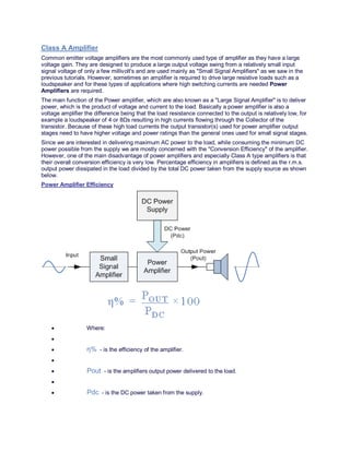
  • 1. Class A Amplifier Common emitter voltage amplifiers are the most commonly used type of amplifier as they have a large voltage gain. They are designed to produce a large output voltage swing from a relatively small input signal voltage of only a few millivolt's and are used mainly as "Small Signal Amplifiers" as we saw in the previous tutorials. However, sometimes an amplifier is required to drive large resistive loads such as a loudspeaker and for these types of applications where high switching currents are needed Power Amplifiers are required. The main function of the Power amplifier, which are also known as a "Large Signal Amplifier" is to deliver power, which is the product of voltage and current to the load. Basically a power amplifier is also a voltage amplifier the difference being that the load resistance connected to the output is relatively low, for example a loudspeaker of 4 or 8Ωs resulting in high currents flowing through the Collector of the transistor. Because of these high load currents the output transistor(s) used for power amplifier output stages need to have higher voltage and power ratings than the general ones used for small signal stages. Since we are interested in delivering maximum AC power to the load, while consuming the minimum DC power possible from the supply we are mostly concerned with the "Conversion Efficiency" of the amplifier. However, one of the main disadvantage of power amplifiers and especially Class A type amplifiers is that their overall conversion efficiency is very low. Percentage efficiency in amplifiers is defined as the r.m.s. output power dissipated in the load divided by the total DC power taken from the supply source as shown below. Power Amplifier Efficiency ď‚· Where: ď‚· ď‚· η% - is the efficiency of the amplifier. ď‚· ď‚· Pout - is the amplifiers output power delivered to the load. ď‚· ď‚· Pdc - is the DC power taken from the supply.
  • 2. For a power amplifier it is very important that the amplifiers power supply is well designed to provide the maximum available continuous power to the output signal. Class A Amplifier The most commonly used type of power amplifier configuration is the Class A Amplifier. Class A amplifier stages use the transistor in the standard Common Emitter circuit configuration as seen previously, in which the transistor is always biased "ON" so that it conducts during one complete cycle of the input signal waveform producing minimum distortion to the output. This means then that the Class A Amplifierconfiguration is the ideal operating mode, because there can be no crossover or switch-off distortion to the output waveform. Class A power amplifier output stages may use a single transistor or pairs of transistors connected together to share the high load current. Consider the Class A amplifier circuit below. Single-ended Amplifier Circuit This is the simplest type of Class A power amplifier circuit. It uses a single-ended transistor for its output stage with the resistive load connected directly to the Collector terminal. When the transistor switches "ON" it sinks the output current through the Collector resulting in an inevitable voltage drop across the Emitter resistance thereby limiting the negative output capability. The efficiency of this type of circuit is very low (possibly 20%) and delivers small power outputs for a large drain on the DC power supply. A Class A amplifier stage passes the same load current even when no input signal is applied so large heatsinks are needed for the output transistors. However, another simple way to increase the current handling capacity of the circuit while at the same time obtain a greater power gain is to replace the single output transistor with a Darlington Transistor. These types of devices are basically two transistors within a single package, one small "pilot" transistor and another larger "switching" transistor. The big advantage of these devices are that the input impedance is suitably large while the output impedance is relatively low, thereby reducing the power loss and therefore the heat within the switching device. Darlington Transistor Configurations
  • 3. The overall current gain Beta (β) or Hfe value of a Darlington device is the product of the two individual gains of the transistors multiplied together and very high β values along with high Collector currents are possible compared to a single transistor circuit. To improve the full power efficiency of the Class A amplifier it is possible to design the circuit with a transformer connected directly in the Collector circuit to form a circuit called a Transformer Coupled Amplifier. This improves the efficiency of the amplifier by matching the impedance of the load with that of the amplifiers output using the turns ratio (N) of the transformer and an example is given below. Transformer-coupled Amplifier Circuit As the Collector current, Ic is reduced to below the quiescent Q-point set up by the Base bias voltage, due to variations in the Base current, the magnetic flux in the transformer core collapses causing an induced emf in the transformer primary windings. This causes an instantaneous Collector voltage to rise to a value of twice the supply voltage 2Vcc giving a maximum Collector current of twice Ic when the Collector voltage is at its minimum. Then the efficiency of this type of Class A amplifier configuration can be calculated as follows.
  • 4. The r.m.s. Collector voltage is given as: The r.m.s. Collector current is given as: The r.m.s. Power delivered to the load (Pac) is therefore given as: The average power drawn from the supply (Pdc) is given by: and therefore the efficiency of a Transformer-coupled Class A amplifier is given as: This improves the efficiency of the amplifier by matching the impedance of the load with that of the amplifier using the turns ratio of the transformer and efficiencies reaching 40% are possible with most commercially available Class-A type power amplifiers of this type of configuration, but the use of inductive components is best avoided. Also one big disadvantage of this type of circuit is the additional cost and size of the audio transformer required. It is possible to obtain greater power output and efficiency than that of a Class A amplifier by using two transistors in the output stage in a "push-pull" configuration. This type of configuration is called a Class B Amplifier which we will look at in the next tutorial. Class B Amplifiers To improve the full power efficiency of the previous Class A type amplifier it is possible to design the amplifier circuit with two transistors in its output stage producing a "push-pull" type amplifier configuration. Push-pull operation uses two "complementary" transistors, one an NPN- type and the other a PNP-type with both power transistors receiving the same input signal together that is equal in magnitude, but in opposite phase to each other. This results in one transistor only amplifying one half or 1800 of the input waveform while the other transistor amplifies the other half or remaining 1800 of the waveform with the resulting "two-halves" being put back together at the output terminal. This pushing and pulling of the alternating half cycles by the transistors gives this type of circuit its name but they are more commonly known as Class B Amplifiers as shown below. Class B Push-pull Transformer Amplifier Circuit
  • 5. The circuit above shows a standard push-pull amplifier circuit that uses a balanced centre-tapped input transformer, which splits the incoming waveform signal into two equal cycles that are 1800 out of phase with each other and another centre-tapped transformer on the output to recombined the signals and provide the increased power to the load. The transistors used for this type of transformer push-pull amplifier circuit are both NPN transistors with their emitter terminals connected together. Here, the load current is shared between the two power transistor devices as it decreases in one device and increases in the other throughout the signal cycle reducing the output voltage and current to zero. The result is that both halves of the output waveform now swings from zero to twice the quiescent current thereby reducing dissipation. This has the effect of almost doubling the efficiency of the amplifier to around 70%. Assuming that no input signal is present, then each transistor carries the normal quiescent collector current, the value of which is determined by the base bias which is at the cut-off point. If the transformer is accurately centre tapped, then the two collector currents will flow in opposite directions (ideal condition) and there will be no magnetization of the transformer core, thus minimizing the possibility of distortion. When a signal is present across the secondary of the driver transformer T1, the transistor base inputs are in "anti-phase" to each other as shown, thus if TR1 base goes positive driving the transistor into heavy conduction, its collector current will increase but at the same time the base current of TR2 will go negative further into cut-off and the collector current of this transistor decreases by an equal amount and vice versa. Hence negative halves are amplified by one transistor and positive halves by the other transistor giving this push-pull effect. Unlike the DC condition, these AC currents are ADDITIVE resulting in the two output half-cycles being combined to reform the sine-wave in the output transformers primary winding which then appears across the load. Class B Amplifier operation has zero DC bias as the transistors are biased at the cut-off, so each transistor only conducts when the input signal is greater than the base-emitter voltage. Therefore, at zero input there is zero output. This then means that the actual Q-point of a Class B amplifier is on the Vce part of the load line as shown below. Class B Output Characteristics Curves
  • 6. Class B Amplifiers have the advantage over their Class A amplifier cousins in that no current flows through the transistors when they are in their quiescent state (ie, with no input signal), therefore no power is dissipated in the output transistors or transformer when there is no signal present unlike Class A amplifier stages that require significant base bias thereby dissipating lots of heat - even with no input signal. So the overall conversion efficiency ( η ) of the amplifier is greater than that of the equivalent Class A with efficiencies reaching as high as 75% possible resulting in nearly all modern types of push- pull amplifiers operated in this Class B mode. Transformerless Class B Push-Pull Amplifier One of the main disadvantages of the Class B amplifier circuit above is that it uses balanced centre- tapped transformers in its design, making it expensive to construct. However, there is another type of Class B push-pull amplifier called a Complementary-Symmetry Class B Amplifier that does not use transformers in its design therefore, it is transformerless using instead complementary pairs of transistors. As transformers are not needed this makes the amplifier circuit much smaller for the same amount of output, also there are no stray magnetic effects or transformer distortion to effect the quality of the output signal. An example of a "transformerless" circuit is given below. Class B Transformerless Output Stage
  • 7. While Class B amplifiers have a much high gain than the Class A types, one of the main disadvantages of class B type push-pull amplifiers is that they suffer from an effect known commonly as Crossover Distortion. This occurs during the transition when the transistors are switching over from one to the other as each transistor does not stop or start conducting exactly at the zero crossover point even if they are specially matched pairs. This is because the output transistors require a base-emitter voltage greater than 0.7v for the bipolar transistor to start conducting which results in both transistors being "OFF" at the same time. One way to eliminate this crossover distortion effect would be to bias both the transistors at a point slightly above their cut-off point. This then would give us what is commonly called an Class AB Amplifier circuit. Transformerless Class AB Push-Pull Amplifier We know that we need the base-emitter voltage to be greater than 0.7v for a silicon bipolar transistor to start conducting, so if we were to replace the two voltage divider biasing resistors connected to the base terminals of the transistors with two silicon Diodes, the biasing voltage applied to the transistors would now be equal to the forward voltage drop of the diode. These two diodes are generally called Biasing Diodes or Compensating Diodes and are chosen to match the characteristics of the matching transistors. The circuit below shows diode biasing. Class AB Amplifier
  • 8. The Class AB Amplifier circuit is a compromise between the Class A and the Class B configurations. This very small diode biasing voltage causes both transistors to slightly conduct even when no input signal is present. An input signal waveform will cause the transistors to operate as normal in their active region thereby eliminating any crossover distortion. A small collector current will flow when there is no input signal but it is much less than that for the Class A amplifier configuration. This means then that the transistor will be "ON" for more than half a cycle of the waveform but much less than a full cycle. The amount of diode biasing voltage present at the base terminal of the transistor can also be increased in multiples by adding additional diodes in series. Crossover Distortion We have seen that one of the main disadvantages of a Class A Amplifier is its low full power efficiency rating. But we also know that we can improve the amplifier and almost double its efficiency simply by changing the output stage of the amplifier to a Class B push-pull type configuration. However, this is great from an efficiency point of view, but most modern Class B amplifiers are transformerless or complementary types with two transistors in their output stage. This results in one main fundamental problem with push-pull amplifiers in that the two transistors do not combine together fully at the output both halves of the waveform due to their unique zero cut-off biasing arrangement. As this problem occurs when the signal changes or "crosses-over" from one transistor to the other at the zero voltage point it produces an amount of "distortion" to the output wave shape. This results in a condition that is commonly called Crossover Distortion. Crossover Distortion produces a zero voltage "flat spot" or "deadband" on the output wave shape as it crosses over from one half of the waveform to the other. The reason for this is that the transition period when the transistors are switching over from one to the other, does not stop or start exactly at the zero crossover point thus causing a small delay between the first transistor turning "OFF" and the second transistor turning "ON". This delay results in both transistors being switched "OFF" at the same instant in time producing an output wave shape as shown below. Crossover Distortion Waveform
  • 9. In order that there should be no distortion of the output waveform we must assume that each transistor starts conducting when its base to emitter voltage rises just above zero, but we know that this is not true because for silicon bipolar transistors the base voltage must reach at least 0.7v before the transistor starts to conduct thereby producing this flat spot. This crossover distortion effect also reduces the overall peak to peak value of the output waveform causing the maximum power output to be reduced as shown below. Non-Linear Transfer Characteristics This effect is less pronounced for large input signals as the input voltage is usually quite large but for smaller input signals it can be more severe causing audio distortion to the amplifier. Pre-biasing the Output The problem of Crossover Distortion can be reduced considerably by applying a slight forward base bias voltage (same idea as seen in the Transistor tutorial) to the bases of the two transistors via the centre-tap of the input transformer, thus the transistors are no longer biased at the zero cut-off point but instead are "Pre-biased" at a level determined by this new biasing voltage.
  • 10. Push-pull Amplifier with Pre-biasing This type of resistor pre-biasing causes one transistor to turn "ON" exactly at the same time as the other transistor turns "OFF" as both transistors are now biased slightly above their original cut-off point. However, to achieve this the bias voltage must be at least twice that of the normal base to emitter voltage to turn "ON" the transistors. This pre-biasing can also be implemented in transformerless amplifiers that use complementary transistors by simply replacing the two potential divider resistors with Biasing Diodesas shown below. Pre-biasing with Diodes
  • 11. This pre-biasing voltage either for a transformer or transformerless amplifier circuit, has the effect of moving the amplifiers Q-point past the original cut-off point thus allowing each transistor to operate within its active region for slightly more than half or 180o of each half cycle. In other words 180o + Bias. This then produces an amplifier circuit commonly called a Class AB Amplifier and its biasing arrangement is given below. Class AB Output Characteristics
  • 12. Distortion Summary Then to summarise, Crossover Distortion occurs in Class B amplifiers because the amplifier is biased at its cut-off point. This then results in BOTH transistors being switched "OFF" at the same instant in time. By applying a small base bias voltage either by using a resistive potential divider circuit or diode biasing this crossover distortion can be greatly reduced or even eliminated completely. The application of a biasing voltage produces another type or class of amplifier circuit commonly called a Class AB Amplifier. Then the difference between a pure Class B amplifier and an improved Class AB amplifier is in the biasing level applied to the output transistors. Therefore, we can say the a Class AB amplifier is a Class B amplifier with Bias and we can summarise as: ď‚· Class A Amplifiers have no Crossover Distortion as they are biased in the centre of the load line. ď‚· ď‚· Class B Amplifiers have large amounts of Crossover Distortion due to biasing at the cut-off point. ď‚· ď‚· Class AB Amplifiers may have some Crossover Distortion if the biasing level is too low. Amplifiers Summary Page
  • 13. Small Signal Amplifiers ď‚· Small Signal Amplifiers are also known as Voltage Amplifiers. ď‚· Voltage Amplifiers have 3 main properties, Input Resistance, Output Resistance and Gain. ď‚· The Gain of a small signal amplifier is the amount by which the amplifier "Amplifies" the input signal. ď‚· Gain is a ratio of input divided by output, therefore it has no units but is given the symbol (A) with the most common types being, Voltage Gain (Av), Current Gain (Ai) and Power Gain (Ap) ď‚· The power Gain of the amplifier can also be expressed in Decibels or simply dB. ď‚· In order to amplify all of the input signal distortion free in a Class A type amplifier, DC Base Biasing is required. ď‚· DC Bias sets the Q-point of the amplifier half way along the load line. ď‚· This DC Base biasing means that the amplifier consumes power even if there is no input signal present. ď‚· The transistor amplifier is non-linear and an incorrect bias setting will produce large amounts of distortion to the output waveform. ď‚· Too large an input signal will produce large amounts of distortion due to clipping, which is also a form of amplitude distortion. ď‚· Incorrect positioning of the Q-point on the load line will produce either Saturation Clipping orCut-off Clipping. ď‚· The Common Emitter Amplifier configuration is the most common form of all the general purpose voltage amplifier circuits. Large Signal Amplifiers ď‚· Large Signal Amplifiers are also known as Power Amplifiers. ď‚· Power Amplifiers can be sub-divided into different Classes, for example Class A Amplifiers, where the output device conducts for all of the input cycle, Class B Amplifiers, where the output device conducts for only 50% of the input cycle and Class AB Amplifiers, where the output device conducts for more than 50% but less than 100% of the input cycle. ď‚· An ideal Power Amplifier would deliver 100% of the available DC power to the load. ď‚· Class A amplifiers are the most common form of power amplifier but only have an efficiency rating of less than 40%. ď‚· Class B amplifiers are more efficient than Class A amplifiers at around 70% but produce high amounts of distortion. ď‚· Class B amplifiers consume very little power when there is no input signal present. ď‚· By using the "Push-pull" output stage configuration, distortion can be greatly reduced. ď‚· However, simple push-pull Class B Power amplifiers can produce high levels of Crossover Distortion due to their cut-off point biasing. ď‚· Pre-biasing resistors or diodes will help eliminate this crossover distortion.
  • 14. ď‚· Class B Power Amplifiers can be made using Transformers or Complementary Transistors in its output stage.