SlideShare ist ein Scribd-Unternehmen logo
1 von 6
Unit 4: Special Oscilloscopes
Delayed time base oscilloscope:
        In a conventional oscilloscope, the signal to the vertical plates is delayed by time, using1
delay line circuit. The waveform before the delay circuit is used to trigger the time base. This
allows the study of all the leading or lagging edges of a pulse type waveform. This is shown in
the Figure to triggering of time base by input signal, sweep starts well in time and when input
appears at vertical sections, the sweep is triggered and delayed waveform is displayed.

        The delay ensures that no part of the waveform gets lost. In delayed time base
oscilloscope, a variable time delay circuit is used in the basic time base circuit. This allows the
triggering of sweep time after the delay time. Thus the delay time is variable. This time is
denoted as td. After this, the sweep is triggered for the time t, Then the portion of the waveform
for the time t x gets expanded on the complete oscilloscope screen, for the detail study.


        If input is pulse waveform and leading edge is used to trigger the delay time, then lagging
edge can be displayed to fill the entire oscilloscope screen. This is shown in the Fig (a). Similarly
if the lagging edge is used to trigger the delay time then leading edge will be displayed on the
entire screen for the time tx. This is shown in the Fig.(b). If the time delay is perfectly adjusted,
then any portion of the waveform can be extended to fill the entire screen. This is shown in the
Fig. (c).
The normal time base circuit is main time base (MTB) circuit which functions same as c1
conventional oscilloscope. The function of MTB blanking circuit is to produce an unblanking
pulse which is applied to CRT grid to turn on an electron beam in the CRT, during the display
sweep time. The ramp output of MTB is given to the horizontal deflection amplifier via switch S.
It is also given as one input to the voltage comparator.

        The other input to the voltage comparator is derived from the potentiometer whose level
is adjustable. The unblanking pulses from MTB and DTB are added by summing circuit and
given to the CRT grid. The unblanking pulse of MTB produces a trace of uniform intensity. But
during ramp time of DTB, the addition of two pulses decides the intensity of the trace on the
screen. Hence during DTB time, the voltage applied to CRT grid is almost twice than the voltage
corresponding to MTB time.

         This increases the brightness of the displayed waveform for the DTB time. When the
part of the waveform to be brightened is identified, then the DTB ramp output is connected to the
input of the horizontal deflection amplifier through switch S. The DTB ramp time is much
smaller than MTB period but its amplitude (- V to + V) is same as MTB ramp.

        hence it causes the oscilloscope electron beam to be deflected from one side of the screen
to the other, during short DTB time. By adjusting DTB time/ div control, the brightened portion
can be extended, so as to fill the entire screen of the oscilloscope. The horizontal deflection starts
only after the delay time t d from the beginning of the MTB sweep. Thus very small part of the
waveform can be extended on the entire screen. Waveforms of the Delayed Time Base
Oscilloscope The waveforms of the delayed time base oscilloscope are shown in the Fig.
Analog storage oscilloscope:
        The conventional cathode ray tube has the persistence of the phosphor ranging from a
Few millisecond to several seconds. But sometimes it is necessary to retain the image for much
'longer periods, upto several hours. It requires storing of a waveform for a certain duration,'
independent of phosphor persistence. Such a retention property helps to display the waveforms
of very low frequency. Mainly two types of storage techniques are used in cathode ray tubes
which are:
i) Mesh storage and ii) Phosphor storage

Sampling Time Base: The time base circuit of the sampling oscilloscope is different than the
conventional oscilloscope. The time base of sampling oscilloscope has two functions: i) To move
the dots across the screen ii) To generate the sampling command pulses for the sampling circuit.

       It consists of synchronous circuit, which determines the sampling rate and establishes a
reference point in time with respect to the input signal. The time base generates a triggering
pulse which activates the oscillator to generate a ramp voltage. Similarly it generates a stair case
waveform. The ramp generation is based on the output of the synchronizing circuit.

        Both the ramp as well as staircase waveforms are applied to a voltage comparator. This
comparator compares the two voltages and whenever these two voltages are equal, it generates a
samppng pulse. This pulse then momentarily bias the diodes of the sampling gate in the forward
direction and thus diode switch gets closed for short duration of time.
The capacitor charges but for short time hence, it can charge to only a small percentage
of the input signal value at that instant. This voltage is amplified by the vertical amplifier and
then applied to the vertical deflecting plates. This is nothing but a sample. At the same time, the
comparator gives a signal to the staircase generator to advance through one step. This is applied
to horizontal deflecting plates, thus during each step of the stair case waveform, the spot moves
across the screen. Thus the sampling time base is called a staircase-ramp generator in case of a
sampling oscillosope.

Block diagram of Sampling Oscilloscope:

The block diagram of sampling oscilloscope is shown in the Fig.


        The input signal is applied to the diode sampling gate. At the start of each sampling cycle
a trigger input pulse is generated which activates the blocking oscillator. The oscillator output is
given to the ramp generator which generates the linear ramp signal. Since the sampling must be
synchronized with the input signal frequency, the signal is delayed in the vertical amplifier.

       The staircase generator produces a staircase waveform which is applied to an attenuator.
The attenuator controls the magnitude of the staircase signal and then it is applied to a voltage
comparator. Another input to the voltage comparator is the output of the ramp generator. The
voltage comparator compares the two signals and produces the output pulse when the two
voltages are equal. This is nothing but a sampling pulse which is applied to sampling gate
through the gate control circuitry. This pulse opens the diode gate and sample is taken in.

        This sampled signal is then applied to the vertical amplifier and the vertical deflecting
plates. The output of the staircase generator is also applied to the horizontal deflecting plates.
During each step of staircase the spot moves on the screen. The comparator output advances the
staircase output through one step. After certain number of pulses about thousand or so, the
staircase generator resets. The smaller the size of the steps of the staircase generator, larger is the
number of samples and higher is the resolution of the image.

Digital Storage Oscilloscope:
In this digital storage oscilloscope, the waveform to be stored is digitized and then stored in a
digital memory. The conventional cathode ray tube is used in this oscilloscope hence the cost is
less. The power to be applied to memory is small and can be supplied by small battery. Due to
this the stored image can be displayed indefinitely as long ,15 power is supplied to memory.
Once the waveform is digitized then it can be further loaded into the computer and can be
analysed in detail.

Block Diagram: The block diagram of digital storage oscilloscope is shown in the Fig.


        As done in all the oscilloscopes, the input signal is applied to the amplifier and attenuator
section. The oscilloscope uses same type of amplifier and attenuator circuitry as used in the
conventional oscilloscopes. The attenuated signal is then applied to the vertical amplifier.
The vertical input, after passing through the vertical amplifier, is digitised by an analog to
digital converter to create a data set that is stored in the memory. The data set is processed by the
microprocessor and then sent to the display. To digitise the analog signal, analog to digital (AID)
converter is used. The output of the vertical amplifier is applied to the AID converter section.
The main requirement of AID converter in the digital storage oscilloscope is its speed, while in
digital voltmeters accuracy and resolution were the main requirements. The digitised output
needed only in the binary form and not in BCD. The successive approximation type of AID
converter is most oftenly used in the digital storage oscilloscopes.

Modes of operation: The digital storage oscilloscope has three modes of operation:

   1. Roll mode ii) Store mode iii) Hold or save mode.

Roll mode: This mode is used to display very fast varying signals, clearly on the screen. The fast
varying signal is displayed as if it is changing slowly, on the screen. In this mode, the input
signal is not triggered at all.

Weitere ähnliche Inhalte

Was ist angesagt?

IMPLEMENTATION OF UPSAMPLING & DOWNSAMPLING
IMPLEMENTATION OF UPSAMPLING & DOWNSAMPLINGIMPLEMENTATION OF UPSAMPLING & DOWNSAMPLING
IMPLEMENTATION OF UPSAMPLING & DOWNSAMPLINGFAIZAN SHAFI
 
Frequency-Shift Keying
Frequency-Shift KeyingFrequency-Shift Keying
Frequency-Shift KeyingJessie Rama
 
Linear modulation
Linear modulation Linear modulation
Linear modulation Punk Pankaj
 
Smart Antenna for mobile communication
Smart Antenna for mobile communicationSmart Antenna for mobile communication
Smart Antenna for mobile communicationYasoob raza
 
Vlsi lab viva question with answers
Vlsi lab viva question with answersVlsi lab viva question with answers
Vlsi lab viva question with answersAyesha Ambreen
 
4.5 equalizers and its types
4.5   equalizers and its types4.5   equalizers and its types
4.5 equalizers and its typesJAIGANESH SEKAR
 
Stability of Control System
Stability of Control SystemStability of Control System
Stability of Control Systemvaibhav jindal
 
Successive Approximation ADC
Successive Approximation ADC Successive Approximation ADC
Successive Approximation ADC AbhayDhupar
 
Double Side band Suppressed carrier (DSB-SC) Modulation and Demodulation.
 Double Side band Suppressed carrier (DSB-SC) Modulation and Demodulation. Double Side band Suppressed carrier (DSB-SC) Modulation and Demodulation.
Double Side band Suppressed carrier (DSB-SC) Modulation and Demodulation.SAiFul IslAm
 
M ary psk and m ary qam ppt
M ary psk and m ary qam pptM ary psk and m ary qam ppt
M ary psk and m ary qam pptDANISHAMIN950
 
PSK (PHASE SHIFT KEYING )
PSK (PHASE SHIFT KEYING )PSK (PHASE SHIFT KEYING )
PSK (PHASE SHIFT KEYING )vijidhivi
 
SIGNAL CHARACTERISTICS
SIGNAL CHARACTERISTICSSIGNAL CHARACTERISTICS
SIGNAL CHARACTERISTICSRUpaliLohar
 
Vestigial side band (vsb)
Vestigial side band (vsb)Vestigial side band (vsb)
Vestigial side band (vsb)ggpriya me
 

Was ist angesagt? (20)

IMPLEMENTATION OF UPSAMPLING & DOWNSAMPLING
IMPLEMENTATION OF UPSAMPLING & DOWNSAMPLINGIMPLEMENTATION OF UPSAMPLING & DOWNSAMPLING
IMPLEMENTATION OF UPSAMPLING & DOWNSAMPLING
 
Frequency-Shift Keying
Frequency-Shift KeyingFrequency-Shift Keying
Frequency-Shift Keying
 
Linear modulation
Linear modulation Linear modulation
Linear modulation
 
Handoff
HandoffHandoff
Handoff
 
Smart Antenna for mobile communication
Smart Antenna for mobile communicationSmart Antenna for mobile communication
Smart Antenna for mobile communication
 
ASK,FSK and M-PSK using Matlab
ASK,FSK and M-PSK using MatlabASK,FSK and M-PSK using Matlab
ASK,FSK and M-PSK using Matlab
 
Vlsi lab viva question with answers
Vlsi lab viva question with answersVlsi lab viva question with answers
Vlsi lab viva question with answers
 
4.5 equalizers and its types
4.5   equalizers and its types4.5   equalizers and its types
4.5 equalizers and its types
 
Amplitude modulation
Amplitude modulationAmplitude modulation
Amplitude modulation
 
Stability of Control System
Stability of Control SystemStability of Control System
Stability of Control System
 
Emi unit iii ppt
Emi unit iii pptEmi unit iii ppt
Emi unit iii ppt
 
Successive Approximation ADC
Successive Approximation ADC Successive Approximation ADC
Successive Approximation ADC
 
Double Side band Suppressed carrier (DSB-SC) Modulation and Demodulation.
 Double Side band Suppressed carrier (DSB-SC) Modulation and Demodulation. Double Side band Suppressed carrier (DSB-SC) Modulation and Demodulation.
Double Side band Suppressed carrier (DSB-SC) Modulation and Demodulation.
 
M ary psk and m ary qam ppt
M ary psk and m ary qam pptM ary psk and m ary qam ppt
M ary psk and m ary qam ppt
 
Adaptive equalization
Adaptive equalizationAdaptive equalization
Adaptive equalization
 
PSK (PHASE SHIFT KEYING )
PSK (PHASE SHIFT KEYING )PSK (PHASE SHIFT KEYING )
PSK (PHASE SHIFT KEYING )
 
Pll ppt
Pll pptPll ppt
Pll ppt
 
SIGNAL CHARACTERISTICS
SIGNAL CHARACTERISTICSSIGNAL CHARACTERISTICS
SIGNAL CHARACTERISTICS
 
Vestigial side band (vsb)
Vestigial side band (vsb)Vestigial side band (vsb)
Vestigial side band (vsb)
 
Amplitude modulation
Amplitude modulationAmplitude modulation
Amplitude modulation
 

Andere mochten auch

Hv instructions
Hv instructionsHv instructions
Hv instructionsfriends
 
Eltherm ELSR-Ramp Heat Trace Cable - Spec Sheet
Eltherm ELSR-Ramp Heat Trace Cable - Spec SheetEltherm ELSR-Ramp Heat Trace Cable - Spec Sheet
Eltherm ELSR-Ramp Heat Trace Cable - Spec SheetThorne & Derrick UK
 
DC Power Analyzer, Modular, 600W and Four Slots: N6705A
DC Power Analyzer, Modular, 600W and   Four Slots: N6705ADC Power Analyzer, Modular, 600W and   Four Slots: N6705A
DC Power Analyzer, Modular, 600W and Four Slots: N6705APremier Farnell
 
ADC - Dual Slope Integrator
ADC - Dual Slope IntegratorADC - Dual Slope Integrator
ADC - Dual Slope IntegratorManjunath Meti
 
Function Generator
Function GeneratorFunction Generator
Function Generatorraj singh
 
Back corona model
Back corona model Back corona model
Back corona model IRS srl
 
Cro (emmi) (1)
Cro (emmi) (1)Cro (emmi) (1)
Cro (emmi) (1)Ravi Anand
 
Embarquer Linux et des systèmes libres, méthodes et apports
Embarquer Linux et des systèmes libres, méthodes et apportsEmbarquer Linux et des systèmes libres, méthodes et apports
Embarquer Linux et des systèmes libres, méthodes et apportsguest3be047
 
Tracabilite & Identification Automatique par Bernard JEANNE-BEYLOT @JB Thèque
Tracabilite & Identification Automatique par Bernard JEANNE-BEYLOT @JB ThèqueTracabilite & Identification Automatique par Bernard JEANNE-BEYLOT @JB Thèque
Tracabilite & Identification Automatique par Bernard JEANNE-BEYLOT @JB ThèqueBernard Jeanne-Beylot
 
Séminaire Captronic Yocto 24 février 2015
Séminaire Captronic Yocto 24 février 2015Séminaire Captronic Yocto 24 février 2015
Séminaire Captronic Yocto 24 février 2015Christian Charreyre
 
Concevoir un système Linux embarqué avec Yocto Project
Concevoir un système Linux embarqué avec Yocto ProjectConcevoir un système Linux embarqué avec Yocto Project
Concevoir un système Linux embarqué avec Yocto ProjectChristian Charreyre
 
Tasich-Koyani, Mindy, Conestoga-Rovers Associates, Waste Reduction Strategies...
Tasich-Koyani, Mindy, Conestoga-Rovers Associates, Waste Reduction Strategies...Tasich-Koyani, Mindy, Conestoga-Rovers Associates, Waste Reduction Strategies...
Tasich-Koyani, Mindy, Conestoga-Rovers Associates, Waste Reduction Strategies...Kevin Perry
 
ROUSH CleanTech Propane Autogas Vehicles
ROUSH CleanTech Propane Autogas VehiclesROUSH CleanTech Propane Autogas Vehicles
ROUSH CleanTech Propane Autogas VehiclesWisconsin Clean Cities
 
Meet ROUSH CleanTech - BNA Airport Pres.
Meet ROUSH CleanTech - BNA Airport Pres.Meet ROUSH CleanTech - BNA Airport Pres.
Meet ROUSH CleanTech - BNA Airport Pres.ETCleanFuels
 

Andere mochten auch (20)

Hv instructions
Hv instructionsHv instructions
Hv instructions
 
Eltherm ELSR-Ramp Heat Trace Cable - Spec Sheet
Eltherm ELSR-Ramp Heat Trace Cable - Spec SheetEltherm ELSR-Ramp Heat Trace Cable - Spec Sheet
Eltherm ELSR-Ramp Heat Trace Cable - Spec Sheet
 
DC Power Analyzer, Modular, 600W and Four Slots: N6705A
DC Power Analyzer, Modular, 600W and   Four Slots: N6705ADC Power Analyzer, Modular, 600W and   Four Slots: N6705A
DC Power Analyzer, Modular, 600W and Four Slots: N6705A
 
ADC - Dual Slope Integrator
ADC - Dual Slope IntegratorADC - Dual Slope Integrator
ADC - Dual Slope Integrator
 
tca785
tca785tca785
tca785
 
ABB Instrumentation Overview
ABB Instrumentation OverviewABB Instrumentation Overview
ABB Instrumentation Overview
 
Function Generator
Function GeneratorFunction Generator
Function Generator
 
Back corona model
Back corona model Back corona model
Back corona model
 
Cro (emmi) (1)
Cro (emmi) (1)Cro (emmi) (1)
Cro (emmi) (1)
 
Energie maison
Energie maisonEnergie maison
Energie maison
 
Embarquer Linux et des systèmes libres, méthodes et apports
Embarquer Linux et des systèmes libres, méthodes et apportsEmbarquer Linux et des systèmes libres, méthodes et apports
Embarquer Linux et des systèmes libres, méthodes et apports
 
Tracabilite & Identification Automatique par Bernard JEANNE-BEYLOT @JB Thèque
Tracabilite & Identification Automatique par Bernard JEANNE-BEYLOT @JB ThèqueTracabilite & Identification Automatique par Bernard JEANNE-BEYLOT @JB Thèque
Tracabilite & Identification Automatique par Bernard JEANNE-BEYLOT @JB Thèque
 
Séminaire Captronic Yocto 24 février 2015
Séminaire Captronic Yocto 24 février 2015Séminaire Captronic Yocto 24 février 2015
Séminaire Captronic Yocto 24 février 2015
 
Concevoir un système Linux embarqué avec Yocto Project
Concevoir un système Linux embarqué avec Yocto ProjectConcevoir un système Linux embarqué avec Yocto Project
Concevoir un système Linux embarqué avec Yocto Project
 
Tasich-Koyani, Mindy, Conestoga-Rovers Associates, Waste Reduction Strategies...
Tasich-Koyani, Mindy, Conestoga-Rovers Associates, Waste Reduction Strategies...Tasich-Koyani, Mindy, Conestoga-Rovers Associates, Waste Reduction Strategies...
Tasich-Koyani, Mindy, Conestoga-Rovers Associates, Waste Reduction Strategies...
 
Lng as marine fuel norway
Lng as marine fuel   norwayLng as marine fuel   norway
Lng as marine fuel norway
 
ROUSH CleanTech Propane Autogas Vehicles
ROUSH CleanTech Propane Autogas VehiclesROUSH CleanTech Propane Autogas Vehicles
ROUSH CleanTech Propane Autogas Vehicles
 
Lpg
LpgLpg
Lpg
 
Meet ROUSH CleanTech - BNA Airport Pres.
Meet ROUSH CleanTech - BNA Airport Pres.Meet ROUSH CleanTech - BNA Airport Pres.
Meet ROUSH CleanTech - BNA Airport Pres.
 
AIR FLOW DETECTOR SYSTEM
AIR FLOW DETECTOR SYSTEMAIR FLOW DETECTOR SYSTEM
AIR FLOW DETECTOR SYSTEM
 

Ähnlich wie Unit 4 ei

Analog electronics LAB MANUAL
Analog electronics LAB MANUALAnalog electronics LAB MANUAL
Analog electronics LAB MANUALAJAL A J
 
Lissajous pattern
Lissajous patternLissajous pattern
Lissajous patternashmad
 
Lissajous pattern
Lissajous patternLissajous pattern
Lissajous patternashmad
 
1.Oscilloscope. 2.Block diagram of Oscilloscope. 3.Types of Oscilloscope. 4.A...
1.Oscilloscope. 2.Block diagram of Oscilloscope. 3.Types of Oscilloscope. 4.A...1.Oscilloscope. 2.Block diagram of Oscilloscope. 3.Types of Oscilloscope. 4.A...
1.Oscilloscope. 2.Block diagram of Oscilloscope. 3.Types of Oscilloscope. 4.A...AL- AMIN
 
cathode ray oscilloscope &function generator
cathode ray oscilloscope &function generatorcathode ray oscilloscope &function generator
cathode ray oscilloscope &function generatormegha agrawal
 
Cathode ray oscilloscope
Cathode ray oscilloscopeCathode ray oscilloscope
Cathode ray oscilloscopeesmaeel21
 
157929707-Presentation-on-Cro.pptx
157929707-Presentation-on-Cro.pptx157929707-Presentation-on-Cro.pptx
157929707-Presentation-on-Cro.pptxpranjalmishra68
 
Report on speed control of d.c. motor using pwm method
Report on speed control of d.c. motor using pwm methodReport on speed control of d.c. motor using pwm method
Report on speed control of d.c. motor using pwm methodshivam singh
 
Cathode Ray Oscilloscope
Cathode Ray OscilloscopeCathode Ray Oscilloscope
Cathode Ray Oscilloscoperajainayat
 
Design of Counter Using SRAM
Design of Counter Using SRAMDesign of Counter Using SRAM
Design of Counter Using SRAMIOSRJECE
 
Halderman ch043 lecture
Halderman ch043 lectureHalderman ch043 lecture
Halderman ch043 lecturemcfalltj
 
CRO and functional generator physics
CRO and functional generator physicsCRO and functional generator physics
CRO and functional generator physicsAbdul Wahab Raza
 
AREA OPTIMIZED FPGA IMPLEMENTATION FOR GENERATION OF RADAR PULSE COM-PRESSION...
AREA OPTIMIZED FPGA IMPLEMENTATION FOR GENERATION OF RADAR PULSE COM-PRESSION...AREA OPTIMIZED FPGA IMPLEMENTATION FOR GENERATION OF RADAR PULSE COM-PRESSION...
AREA OPTIMIZED FPGA IMPLEMENTATION FOR GENERATION OF RADAR PULSE COM-PRESSION...VLSICS Design
 
Project_Kaveh & Mohammad
Project_Kaveh & MohammadProject_Kaveh & Mohammad
Project_Kaveh & MohammadKaveh Dehno
 

Ähnlich wie Unit 4 ei (20)

CRO
CROCRO
CRO
 
Analog electronics LAB MANUAL
Analog electronics LAB MANUALAnalog electronics LAB MANUAL
Analog electronics LAB MANUAL
 
Lissajous pattern
Lissajous patternLissajous pattern
Lissajous pattern
 
Lissajous pattern
Lissajous patternLissajous pattern
Lissajous pattern
 
1.Oscilloscope. 2.Block diagram of Oscilloscope. 3.Types of Oscilloscope. 4.A...
1.Oscilloscope. 2.Block diagram of Oscilloscope. 3.Types of Oscilloscope. 4.A...1.Oscilloscope. 2.Block diagram of Oscilloscope. 3.Types of Oscilloscope. 4.A...
1.Oscilloscope. 2.Block diagram of Oscilloscope. 3.Types of Oscilloscope. 4.A...
 
cathode ray oscilloscope &function generator
cathode ray oscilloscope &function generatorcathode ray oscilloscope &function generator
cathode ray oscilloscope &function generator
 
DSO.pptx
DSO.pptxDSO.pptx
DSO.pptx
 
Cathode ray oscilloscope
Cathode ray oscilloscopeCathode ray oscilloscope
Cathode ray oscilloscope
 
157929707-Presentation-on-Cro.pptx
157929707-Presentation-on-Cro.pptx157929707-Presentation-on-Cro.pptx
157929707-Presentation-on-Cro.pptx
 
Oscilloscope tutorial
Oscilloscope tutorialOscilloscope tutorial
Oscilloscope tutorial
 
Emi unit ii ppt
Emi unit ii pptEmi unit ii ppt
Emi unit ii ppt
 
Report on speed control of d.c. motor using pwm method
Report on speed control of d.c. motor using pwm methodReport on speed control of d.c. motor using pwm method
Report on speed control of d.c. motor using pwm method
 
unit 4.pdf
unit 4.pdfunit 4.pdf
unit 4.pdf
 
Cathode Ray Oscilloscope
Cathode Ray OscilloscopeCathode Ray Oscilloscope
Cathode Ray Oscilloscope
 
Design of Counter Using SRAM
Design of Counter Using SRAMDesign of Counter Using SRAM
Design of Counter Using SRAM
 
Halderman ch043 lecture
Halderman ch043 lectureHalderman ch043 lecture
Halderman ch043 lecture
 
CRO and FG.ppt
CRO and FG.pptCRO and FG.ppt
CRO and FG.ppt
 
CRO and functional generator physics
CRO and functional generator physicsCRO and functional generator physics
CRO and functional generator physics
 
AREA OPTIMIZED FPGA IMPLEMENTATION FOR GENERATION OF RADAR PULSE COM-PRESSION...
AREA OPTIMIZED FPGA IMPLEMENTATION FOR GENERATION OF RADAR PULSE COM-PRESSION...AREA OPTIMIZED FPGA IMPLEMENTATION FOR GENERATION OF RADAR PULSE COM-PRESSION...
AREA OPTIMIZED FPGA IMPLEMENTATION FOR GENERATION OF RADAR PULSE COM-PRESSION...
 
Project_Kaveh & Mohammad
Project_Kaveh & MohammadProject_Kaveh & Mohammad
Project_Kaveh & Mohammad
 

Unit 4 ei

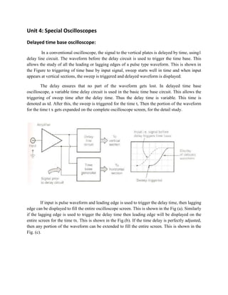
  • 1. Unit 4: Special Oscilloscopes Delayed time base oscilloscope: In a conventional oscilloscope, the signal to the vertical plates is delayed by time, using1 delay line circuit. The waveform before the delay circuit is used to trigger the time base. This allows the study of all the leading or lagging edges of a pulse type waveform. This is shown in the Figure to triggering of time base by input signal, sweep starts well in time and when input appears at vertical sections, the sweep is triggered and delayed waveform is displayed. The delay ensures that no part of the waveform gets lost. In delayed time base oscilloscope, a variable time delay circuit is used in the basic time base circuit. This allows the triggering of sweep time after the delay time. Thus the delay time is variable. This time is denoted as td. After this, the sweep is triggered for the time t, Then the portion of the waveform for the time t x gets expanded on the complete oscilloscope screen, for the detail study. If input is pulse waveform and leading edge is used to trigger the delay time, then lagging edge can be displayed to fill the entire oscilloscope screen. This is shown in the Fig (a). Similarly if the lagging edge is used to trigger the delay time then leading edge will be displayed on the entire screen for the time tx. This is shown in the Fig.(b). If the time delay is perfectly adjusted, then any portion of the waveform can be extended to fill the entire screen. This is shown in the Fig. (c).
  • 2. The normal time base circuit is main time base (MTB) circuit which functions same as c1 conventional oscilloscope. The function of MTB blanking circuit is to produce an unblanking pulse which is applied to CRT grid to turn on an electron beam in the CRT, during the display sweep time. The ramp output of MTB is given to the horizontal deflection amplifier via switch S. It is also given as one input to the voltage comparator. The other input to the voltage comparator is derived from the potentiometer whose level is adjustable. The unblanking pulses from MTB and DTB are added by summing circuit and given to the CRT grid. The unblanking pulse of MTB produces a trace of uniform intensity. But during ramp time of DTB, the addition of two pulses decides the intensity of the trace on the screen. Hence during DTB time, the voltage applied to CRT grid is almost twice than the voltage corresponding to MTB time. This increases the brightness of the displayed waveform for the DTB time. When the part of the waveform to be brightened is identified, then the DTB ramp output is connected to the input of the horizontal deflection amplifier through switch S. The DTB ramp time is much smaller than MTB period but its amplitude (- V to + V) is same as MTB ramp. hence it causes the oscilloscope electron beam to be deflected from one side of the screen to the other, during short DTB time. By adjusting DTB time/ div control, the brightened portion can be extended, so as to fill the entire screen of the oscilloscope. The horizontal deflection starts only after the delay time t d from the beginning of the MTB sweep. Thus very small part of the waveform can be extended on the entire screen. Waveforms of the Delayed Time Base Oscilloscope The waveforms of the delayed time base oscilloscope are shown in the Fig.
  • 3. Analog storage oscilloscope: The conventional cathode ray tube has the persistence of the phosphor ranging from a Few millisecond to several seconds. But sometimes it is necessary to retain the image for much 'longer periods, upto several hours. It requires storing of a waveform for a certain duration,' independent of phosphor persistence. Such a retention property helps to display the waveforms of very low frequency. Mainly two types of storage techniques are used in cathode ray tubes which are: i) Mesh storage and ii) Phosphor storage Sampling Time Base: The time base circuit of the sampling oscilloscope is different than the conventional oscilloscope. The time base of sampling oscilloscope has two functions: i) To move the dots across the screen ii) To generate the sampling command pulses for the sampling circuit. It consists of synchronous circuit, which determines the sampling rate and establishes a reference point in time with respect to the input signal. The time base generates a triggering pulse which activates the oscillator to generate a ramp voltage. Similarly it generates a stair case waveform. The ramp generation is based on the output of the synchronizing circuit. Both the ramp as well as staircase waveforms are applied to a voltage comparator. This comparator compares the two voltages and whenever these two voltages are equal, it generates a samppng pulse. This pulse then momentarily bias the diodes of the sampling gate in the forward direction and thus diode switch gets closed for short duration of time.
  • 4. The capacitor charges but for short time hence, it can charge to only a small percentage of the input signal value at that instant. This voltage is amplified by the vertical amplifier and then applied to the vertical deflecting plates. This is nothing but a sample. At the same time, the comparator gives a signal to the staircase generator to advance through one step. This is applied to horizontal deflecting plates, thus during each step of the stair case waveform, the spot moves across the screen. Thus the sampling time base is called a staircase-ramp generator in case of a sampling oscillosope. Block diagram of Sampling Oscilloscope: The block diagram of sampling oscilloscope is shown in the Fig. The input signal is applied to the diode sampling gate. At the start of each sampling cycle a trigger input pulse is generated which activates the blocking oscillator. The oscillator output is given to the ramp generator which generates the linear ramp signal. Since the sampling must be synchronized with the input signal frequency, the signal is delayed in the vertical amplifier. The staircase generator produces a staircase waveform which is applied to an attenuator. The attenuator controls the magnitude of the staircase signal and then it is applied to a voltage comparator. Another input to the voltage comparator is the output of the ramp generator. The voltage comparator compares the two signals and produces the output pulse when the two voltages are equal. This is nothing but a sampling pulse which is applied to sampling gate through the gate control circuitry. This pulse opens the diode gate and sample is taken in. This sampled signal is then applied to the vertical amplifier and the vertical deflecting plates. The output of the staircase generator is also applied to the horizontal deflecting plates. During each step of staircase the spot moves on the screen. The comparator output advances the staircase output through one step. After certain number of pulses about thousand or so, the
  • 5. staircase generator resets. The smaller the size of the steps of the staircase generator, larger is the number of samples and higher is the resolution of the image. Digital Storage Oscilloscope: In this digital storage oscilloscope, the waveform to be stored is digitized and then stored in a digital memory. The conventional cathode ray tube is used in this oscilloscope hence the cost is less. The power to be applied to memory is small and can be supplied by small battery. Due to this the stored image can be displayed indefinitely as long ,15 power is supplied to memory. Once the waveform is digitized then it can be further loaded into the computer and can be analysed in detail. Block Diagram: The block diagram of digital storage oscilloscope is shown in the Fig. As done in all the oscilloscopes, the input signal is applied to the amplifier and attenuator section. The oscilloscope uses same type of amplifier and attenuator circuitry as used in the conventional oscilloscopes. The attenuated signal is then applied to the vertical amplifier.
  • 6. The vertical input, after passing through the vertical amplifier, is digitised by an analog to digital converter to create a data set that is stored in the memory. The data set is processed by the microprocessor and then sent to the display. To digitise the analog signal, analog to digital (AID) converter is used. The output of the vertical amplifier is applied to the AID converter section. The main requirement of AID converter in the digital storage oscilloscope is its speed, while in digital voltmeters accuracy and resolution were the main requirements. The digitised output needed only in the binary form and not in BCD. The successive approximation type of AID converter is most oftenly used in the digital storage oscilloscopes. Modes of operation: The digital storage oscilloscope has three modes of operation: 1. Roll mode ii) Store mode iii) Hold or save mode. Roll mode: This mode is used to display very fast varying signals, clearly on the screen. The fast varying signal is displayed as if it is changing slowly, on the screen. In this mode, the input signal is not triggered at all.