Microsystems |Technologies
•
1 like•647 views

Discusses about Microsystems Technologies,micromachining,polymer techniques,photolithography and mask design, wet and dry bulk etching, bonding, thin film deposition and removal, metallization, sacrificial processes, other inorganic processes, electroplating,polymer materials and basics, thick-film polymers, soft lithography and multiple methods of micromolding, stereolithography, LIGA

Recommended
More Related Content
Viewers also liked
Viewers also liked (16)
Similar to Microsystems |Technologies
Similar to Microsystems |Technologies (20)
Recently uploaded
Recently uploaded (20)
Microsystems |Technologies
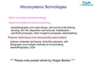
- 1. Microsystems Technologies Basic concepts and terminology Selected traditional micromachining photolithography and mask design, wet and dry bulk etching, bonding, thin film deposition and removal, metallization, sacrificial processes, other inorganic processes, electroplating Polymer techniques (not neccesarilly exact order() polymer materials and basics, thick-film polymers, soft lithography and multiple methods of micromolding, stereolithography, LIGA *** Please note posted article by Holger Becker ***
- 2. Polymer Microfabrication Methods Introduction: polymer materials and basics Various polymers and their characteristics General polymer definitions Thick film mask patternable polymers Including SU-8 photo-epoxy, polysiloxane, polyimide, and PMMA Electroforming using polymer thick films; LIGA Stereolithography Micromolding Soft lithography Hot embossing Other micromolding processes (injection-molding, etc.) Polymer bonding Other polymer microfabrication Laser methods (photoablation, polymerization) Micromilling CVD Plasma etching Others…
- 3. Polymer Materials and Basics Why micromachine polymers? Inexpensive, especially for mass production Flexible substrates may be needed Many polymers have good transmission spectrums for visible and uv wavelengths Easily molded/mass produced Surface properties easily modified Improved biocompatibility and bioreactivity, nontoxic Chemically inert Thermal and electrical isolation (insulating substrate) High aspect ratio microstructures easily realized (some processes) Problems with micromachining polymers Combining processes with other micromachining substrates/processes (e.g., metal interconnect/electrodes) Still “working the bugs out” (as opposed to mature silicon industry supported by microelectronics)
- 4. Polymer Materials and Basics Polymers Consist of long chains of smaller molecules called monomers Carbon allows formation of long chains example: ethylene (monomer) and polyethylene CH2 (ethylene) …CH2=CH2=CH2( (polyethylene) Monomers must undergo polymerization to create polymers addition polymerization: monomer units directly attach (e.g., polyethylene) condensation polymerization: monomer units are linked by intermolecular reaction that gives off another species and/or use another species to react, e.g., water or simple alcohols examples: polyimides, polyesters, silicones
- 5. Polymer Materials and Basics Polymer structure Linear, branched, or cross-linked/networked Linear polymers are composed of a linear arrangement of identical units. Branched polymers have side chains that branch off the main chain. The size of these side chains can vary. Cross-linked polymers form covalent bonds between adjacent chains at various points using branches. linear branched cross-linked network Network polymers form complex 3D structures. Network example: SU-8 epoxy Linear example: polyethylene
- 6. Polymer Materials and Basics Polymer structure (contiuned) Homopolymer (same monomer repeated, eg . , polyethylene Copolymer (more than one monomer, e.g., ethylene and propylene) Copolymers can be further classified based on the arrangements of Their different monomers monomer #1 monomer #2
- 7. Polymer Materials and Basics Polymer types Thermosplastics (e.g., PS, PE, PVC, PC, PMMA, parylene, PETG) linear or branched polymers that can be melted/softened upon application of heat; harden when cooled soft, plastic behavior at low temp; high viscosity at high temp melting point typically around 120 – 180 C usually soluble in common solvents to make liquid Thermosets (e.g., SU-8, other epoxies) highly cross-linked, often network polymers, but not always (PDMS) some can also be processed using melting require “curing” (heat, radiation) to polymerize (“set”) often come in two parts that when mixed will cure Elastomers (e.g., PDMS - thermoset, PU - thermoplastic) weakly cross-linked polymers; usually large molecular weights called “elastomers” because they are generally elastic (stretchy) can be thermosets or thermoplastics (with associated fabrication)
- 8. Polymer Materials and Basics Polymer examples Polymer example (abbrieviation) Example (typical) micromachining method(s) Polystyrene (PS) Hot embossing, laser ablation Polyvinylchloride(PVC) Hot embossing, laser ablation Polycarbonate (PC) Hot embossing, injection molding, laser ablation Polymethylmethacrylate (PMMA) Hot embossing, injection molding, x-ray lithography, laser ablation Parylene CVD SU-8 Photolithography Polyimide Photolithography, laser ablation, RIE etching Polydimethylsiloxane (PDMS) Soft lithography Photosensitive silicone Photolithography Polyethylene tere-phthalate glycol (PETG) Hot embossing, laser ablation Cyclic olefin polymer (COP) Hot embossing, laser ablation, injection molding
- 9. Polymer Materials and Basics Curing methods for thermosets and elastomers Room temperature curing Heat curing Radiation curing (including photopolymerization) Room temperature curing (RTV, room-temp-vulcanization) One-part formulations usually moisture cure (from surrounding air) In two-part RTV, one part is “curing agent”; cure at room temperature by reacting with eachother and/or moisture Heat curing Initiates or speeds up (two-part) polymerization reactions with thermal energy Radiation curing Initiates polymerization reactions with radiant energy, such as uv light Areas radiated cross-link and remain, while uncured polymer is washed away; hence a negative process (negative photoresist)
- 10. Polymer Materials and Basics Radiation (UV, x-ray, etc.) curing versus heat or room temp curing Some advantages of radiation curing 1. High turn-around (fast processing) 2. Low heat generation (heat-sensitive substrates can be used) 3. Very eco-friendly due to low organic emissions 4. UV cure uses conventional microelectronics equipment Some disadvantages of radiation curing 1. Limited to planar geometries 2. High capital equipment costs, although not too bad for uv cure 3. May not be cost effective for wide applications 4. May have post-cure instability when exposed to direct sunlight 5. Some components are skin irritants
- 11. Polymer Materials and Basics Radiation curing Bond breaking Photons have a fixed energy, ε, given by: ε = hν where h is Planck’s constant (9534 x 10-14 cal-s/mol) and v = c/λ where c is the speed of light and λ is the wavelength Energy and light wavelengths required to break bonds Radiation spectrum Once bonds are broken, they can rearrange into a polymer aided by photoinitiators (PI) in the material that utilize the light energy
- 12. Thick Film Polymers Radiation curing X-ray patterning of PMMAfor LIGA UV-light patterned polymers SU-8 photoepoxy Photopattenable silicone elastomer Photosensitive polyimide
- 13. LIGA LIGAis a method of producing high aspect ratio microstructures consisting of three major steps (the acronym is German): LI– Lithographie (lithography) X-ray lithography produces high aspect ratio primary structures in PMMA(polymethyl-methacrylate) “photoresist”; a thick-film polymer process G– Galvanoformung (electroforming) metal is electroformed into the PMMAstructures, possibly planarized, and released A– Abformung (molding) released metal molds are used to fabricate secondary structures in polymers, metals, or ceramics
- 14. LIGA Process flow Shadow printing using x-rays Special mask blocks xrays overview Exposed areas removed in solution (GG (PMMA) developer*) (Cu-Ti stack) Resist and metal on substrate (Ti) sacrificially etched leaving metal mold free of substrate Electroplating of metal into resist structure (e.g., Ni) Covered with polymer micromolding lectures *Available commercially
- 15. LIGA PMMAthick films PMMAdisc bonded to si substrate 1. 2. PMMAcasting onto substrate Twowidelyusedmethods: solvent bonding of PMMA disc (cut from a sheet) onto silicon substrate Casting of PMMA onto substrate; PMMA/MMA plus an polymerization initiator Results in a stressy film
- 16. LIGAmasks and x-ray lithography X-ray masks must be fabricated using micromachining techniques; they are often a thin membrane of x-ray-transparent material (e.g., 5 μm titanium , 500 μm beryllium, 125 μm polyimide) with an x-ray opaque pattern (e.g., gold) Be “wafer” 15 μm thick Au Opaque metal is then electroformed through the photoresist Pattern is often copied from an optical mask LIGA
- 17. LIGA LIGA masks and x-ray lithography PMMAis exposed using synchrotron x-rays through this mask that hasAu areas opaque to x-rays LIGAphotolithography, from mask materials to the synchrotron x-ray source, is an expensive process
- 18. LIGA Results in breakdown of PMMAbonds bond broken under x-rays Does not reorganize Stripped away in solvent (methyl methacrylate) Thus, is a positive (like photoresist) process PMMAchanges MW when exposed to x-rays PMMAexposure
- 19. LIGA Complex structures 1. Mutiple PMMAlevels for multi-level molds 2. Substrate tilting Multi-level patterning
- 20. LIGA Note: bottom picture is SU-8 not PMMA Complex structures 1. Mutiple PMMAlevels for multi-level molds 2. Substrate tilting Substrate tilting
- 21. LIGA ExampleApplications PMMA microneedles LIGA microtweezers LIGAmicromotor
- 22. SU-8 Thick Film Photopolymer What is SU-8? Negative working epoxy-based uv-patternable photopolymer originally developed by IBM What is so great about SU-8? Patterning using standard uv mask aligner (not x-ray!) Thicknesses 2 μm - 2mm with straight side walls Aspect ratios >25:1 (10:1 more typical) Structures can be used directly, or used to mold others (“poor person’s LIGA” or “uv-LIGA” w/PDMS soft lithography or e-forming) Large number of different formulations/viscosities (thicknesses) Compatible with silicon devices, glass, metal, and other polymers Can be patterned on top of circuits, photodiodes, etc. Chemically inert once cured (also makes it difficult to remove) Good thermal stability Appears to be biocompatible
- 23. SU-8 Thick Film Photopolymer What is in SU-8 resin? Epoxy resin: a bisphenol/formaldehyde novolac co-polymer Solvent: gamma-butyrolactone (GBL) Photoinitiator (PI): triarylium salt In the presence of uv-light, the PI converts to “Lewis acid” which in turn is what drives the polymerization through the opening of the epoxy rings. Example Lewis acid: H+SbF6 - from uv effect on Ar+SbF6 - salt Epoxies are thermosetting polymers containing epoxy rings: O epoxy ring CH2CH CH2
- 24. SU-8 Thick Film Photopolymer SU-8 resin structure O epoxy ring CH2CH CH2 (this figure: no H shown) H Glycidyl ether of bisphenolA(SU-8) bisphenolA: [(CH3)2C(C6H4OH)2] glycidyl ether: overall structure; “novolac” formaldehyde
- 25. SU-8 Thick Film Photopolymer Typical process steps for SU-8 (similar to PR) 1. 2. 3. 4. 5. 6. 7. 8. Substrate preparation Spin coating Soft bake to remove solvents (hot plate) Exposure to uv light (350nm and higher, optimally 365nm) Post exposure bake (PEB) to fully cross-link (hot plate) Develop (hard bake) (removal) (sometimes optional steps in parentheses)
- 26. SU-8 Thick Film Photopolymer Spin-coating Resulting film thickness depends mainly on SU-8 formulation and viscosity Spin speed Manufacturer spin speed curves (often not very accurate) SU-8-2 is Viscosity: the least (4.3x10⁻⁵ m2/s) SU-8-100 is the most (5150x10-5 m2/s)
- 27. SU-8 Thick Film Photopolymer Soft-baking Removes solvent Hot plate recommended as oven baking may form a top “skin” and trap solvent Ramping bake avoids thermal shocks These are Microchem’s Soft bake times (hot plate) suggested times; actual times depend on hot plate conditions Hotplate should be level, otherwise your film may look like this: SU-8 wafer
- 28. SU-8 Thick Film Photopolymer Exposure dose at 365nm for SU-8 1000 Exposure Converts salt into Lewis acid for polymerization Dosage depends on film thickness Explosure for i-line (365 nm) uv source (example)
- 29. SU-8 Thick Film Photopolymer PEB times (hot plate) Post-exposure bake Polymerization step drive by Lewis acid created during exposure Can be performed at lower temperatures (even room temperature), but takes longer Similar pe-cautions as soft-bake These are Microchem’s suggested times; must characterize
- 30. SU-8 Thick Film Photopolymer Development Development times Immersion development at room temp. Special developer contains: 1-methoxy-2-propyl acetate After development, rinse in isopropyl alcohol (IPA); water is death Strong agitation is needed to get into high aspect ratio trenches
- 31. SU-8 Thick Film Photopolymer Hard Bake Not necessary, but if you do: 150-200 ºC , avoid thermal shocks Removal Cross-linked SU-8 is very difficult to remove can easily ruin fabrication equipment if gets inside If an adhesion promoter was used (Omnicoat) can sacrificially etch (e.g., MF319 developer) to lift SU-8 from substrate; can also use other sacrificial polymers Microchem offers a stripper (Nanoremover PG) Other stripping methods: fuming nitric acid O2 plus CF4 (3-25%) using RIE and heated chuck laser ablation
- 32. SU-8 Thick Film Photopolymer Properties of SU-8 Physical Mechanical Electromagnetic and optical Physical
- 33. SU-8 Thick Film Photopolymer Properties of SU-8 Mechanical
- 34. SU-8 Thick Film Photopolymer Dielectric constant: 4.5 at 10MHz 4.2 at 10GHz 1.1x10⁵ V/m 1.67 at 408 nm Breakdown voltage: Refractive index: 1.575 at 1550 nm SU-8 fluorescence SU-8 deep well (60 μm thick) analyte Excitation: 350nm Detection: 450nm Properties of SU-8 Electromagnetic and optical
- 35. SU-8 Thick Film Photopolymer Mutli-level SU-8 Very easy provided top structure does not overhang (e.g., closed microchannels) Methods of fabricating closed SU-8 microfluidic channels ed SU 8 (a) (b) Use of a sacrificial material Embedded metal mask to block uv-light for multiple layer exposures Use of thin-film dry resist materials Exposure using selective proton writing (c) (d) (e) Partial exposure of SU-8 film through careful dosage or wavelength control of conventional uv light
- 36. SU-8 Thick Film Photopolymer Compatibility with photodiodes well SU8 photodiode SU-8 microgripper silicon 2nd SU8 level 1st SU-8 microfluidic valve substrate SU8 level Direct SU-8 applications High-aspect ratio structures
- 37. SU-8 Thick Film Photopolymer SU-8 as a mold Electroforming with SU-8 (uv-LIGA) Surpassing PMMA-based LIGAas it uses conventional equipment and is much, much cheaper Ni structures fabricated with uv-LIGA
- 38. SU-8 Thick Film Photopolymer SU-8 as a mold for other materials PDMS mold form most common mold used in soft lithography (covered with molding notes) SU-8 general web resources (http://mems.gatech.edu/msmawebsite/members/processes/processes_files/SU8/SU-8.htm appears to be dead ®) SU-8 supplier: http://www.microchem.com/ Newer site: http://memscyclopedia.org/su8.html
- 39. Photopatternable Silicone Commercially available (e.g., Dow Corning WL-5000 series) Spin-on, photopatternable silicone Aspect ratio 1.3:1 with 15 μm minimum features Sloping sidewalls on most formualtions (approx. 60º slope) Transparent solution (presumably at least to visible) Patternable with standard uv aligner (i-line or broadband) Thick films (e.g., 50 μm thick) Easily removed DIY concoctions Uncured PDMS mixed with xylenes (solvent) and dimethoxy phenyl acetophenone (DMAP) the photoinitator Spin-on, photopatternable at 420nm Aspect ratio 1:1 Films up to 100 μm thick Also transparent and easily removed
- 40. Photopatternable Silicone Applications Microelectronics: elastic contacts Microfluidics: gaskets Photopatterned PDMS gasket Elastic wafer level interconnects
- 41. Photosensitive Polyimide Commercially available for the microelectronics industry Single spin film thicknesses up to 40 μm Uv-patternable using standard equipment (negative working) Can be used directly or as an electroforming mold Compatible with silicon devices, glass, metal, and other polymers Can be patterned on top of circuits, photodiodes, etc. Chemically inert Good thermal stability Good biocompatibility Complaint polyimide hinges for rigid silicon structures Copper electroformed gear using polyimide mold