SlideShare a Scribd company logo
1 of 86
Download to read offline
Chapter 5. Energetic particles-surface
             interactions
Energetic particles: electron, ion, photon, atoms
1. Scanning Probe Microscopies
   STM, AFM, MFM, EFM, etc.
2. Electron spectroscopy and microscopies
   AES, XPS, UPS, PEEM, LEEM, SEM, TEM
3. Vibrational spectroscopies
    RAIRS, MIR, HREELS
4. Ion spectroscopies
   ISS, RBS, SIMS
5. Others
   TPD or TDS
Tools for Characterization
            Tools for Characterization
• Structural analysis: SEM, TEM, XRD, SAM, SPM, PEEM, LEEM,
                      STXM, SXPEM
• Chemical analysis: AES, XPS, TPD, SIMS, EDX, SPM
• Electronic, optical analysis: UV/VIS, UPS, SPM
• Magnetic analysis: SQUID, SMOKE, SEMPA, SPM
• Vibrational analysis: IR, HREELS, Raman, SPM
• Local physico-chemical probe: SPM

             e, hv, ion      tip      e, hv, ion
Scientific issues in nanotechnologies
          (Nanotech.Res. Directions: IWGN report,1999)


• Fundamental properties of isolated nanostructures
• Fundamental properties of ensemble of isolated nanostructures
• Assemblies of nanoscale building blocks
• Evaluation of concepts for devices and systems
• Nanomanufacturing
• Connecting nanoscience and biology
• Molecular electronics


     Local probes with nm spatial resolution for
                  characterization
Scanning Probe Microcopy
• Scanning Tunneling Microscopy(STM): topography, local DOS
• Atomic Force Microscopy (AFM): topography, force measurement
• Lateral Force Microscopy (LFM): friction
• Magnetic Force Microscopy (MFM): magnetism
• Electrostatic Force Microscopy (EFM): charge distribution
• Nearfield Scanning Optical Microscopy (NSOM): optical properties
• Scanning Capacitance Microscopy (SCM): dielectric constant, doping
• Scanning Thermal Microscopy (SThM): temperature
• Ballistic Electron Emission Microscopy (BEEM): interface structure
• Spin-polarized STM (SP-STM): spin structure
• Scanning Electro-chemical Microscopy (SECM): electrochmistry
• Scanning Tunneling Potentiometry (SPM): potential surface
• Photon Emission STM (PESTM): chemical identification
References of SPM
1. P.Hansma, J. Tersoff, J. App. Phys. 61, R1 (1987)
2. Y. Kuk, P.J. Silvermann, Rev. Sci. Inst. 60, 165 (1989)
3. Scanning Tunneling Microscopy and related methods edited by R.J.
    Behm, N. Garcia, and H. Rohrer (1990)
4. C.J. Chen, Introduction to scanning tunneling spectroscpy (oxford,
    1993)
5. H-J Gudtherodt and R. Wiesendanger(ed.), Scanning tunneling
    microscopy I,II,III (Springer,1991-1993)
6. J.A. Kuby and J.J. Boland, Surf. Sci. Rep. 26, 61 (1996)
7. R.J. Hamers, Scanning Probe Microscopy in Chemistry, J. Phys.
    Chem.100, 13013 (1996)
8. G.S. McCarty and P.S.Weiss, Scanning Probe Studies of Single
    Nanostructures, Chem. Rev. 99, 1983 (1999)
9. C. Bai, Scanning tunneling spectroscopy and its applications
    (Springer, 2000)
10. PSIA, www.psia.co.kr/appnotes/apps.htm
11. ThermoMicroscope, www.thermomicro.com/spmguide/contents.
12. Digital Instrument, www.di.com/app_notes/full_appnotes.htm
13. H.-Y. Nie, publish.uwo.ca/~hnie/mmo/all.html
Interactions used for Imaging in SPM

     (a) Tunneling
         I~exp(kd)                (d) Capacitance
                                     C(d) ~ 1/d


     (b) Forces                    (e) Thermal gradient
         F(d) ~ various             (f) Ion flow
                                       f(d) ?
     (c) Optical near fields
          E ~1/d4
                               Resolution limits
                               •The property probed
                               •The probe size
Comparision of Microscopes

                         106

                                          SEM        OM
    Vertical scale (A)


                                    TEM
                         104


                         102

                          1           STM

                               1     102       104   106
                               Lateral scale (A)
Characteristics of Microscopies
                         OM              SEM/TEM           SPM

 Operation              air,liquid      vacuum           air,liquid,UHV

 Depth of field         small           large            medium

 Lateral resolution      1 µm           1-5nm:SEM        2-10nm: AFM
                                        0.1nm:TEM        0.1nm: STM
 Vertical resolution     N/A            N/A              0.1nm: AFM
                                                         0.01nm: STM
 Magnification           1X-2x10³X      10X-106X         5x10²X- 108X

 Sample                 not completely un-chargeable      surface height
                        transparent    vacuum            <10 mm
                                       compatible
                                        thin film: TEM
 Contrast              absorption      scattering        tunneling
                       reflection      diffraction
Limits of Resolution
    • HM (High Resolution Optical Microscope)
        diffraction limit ~ 150 nm
    • PCM (Phase Contrast Microscope)
        subwave length 배율 가능
    • X-ray Microscope
         λ ∼1Α; Synchrotron radiation and X-ray optics
    • SEM (Scanning Electron Microscopy)
        Focused e-beam size > 3nm
    • TEM (Transmission Electron Microscopy)
        ~1 A; 얇은 박막시료
    • LEEM (Low Electron Emission Microscopy)
        low energy e-beam; 20nm
    • PEEM (Photoemission electron Microscopy)
        lateral resolution~100nm; chemical analysis
    • FIM (Field Ion Microscopy)
         tip 형태 시료
Interaction of Electrons with Sample


                          When 20 KV e-beam is used
                          for Ni(Z=28).

                          • Auger electron :10-30A
                          • Secondary electron: 100A
                          • Backscattering electron
                               : 1-2 µm
                          • X-ray ~ 5 µm
                          • Penetrated electron: 5 µm


       Atomic Number              Interaction
       Accelerating voltage       Volume
       Incidence angle
Principle: Scanning Electron Microscopy (SEM)
                                               •Beam size: a few – 30 A
                                               •Beam Voltage: 20-40kV
                                               •Resolution: 10-100 A
                                               •Magnification: 20x-650,000x
                                               •Imaging radiations: Secondary electrons,
                                                     backscattering electrons
                                               •Topographic contrast: Inclination effect,
                                                     shadowing, edge contrast,
                         E-gun
                                               •Composition contrast: backscattering
                                                     yield ~ bulk composition
    Lens                    Detectors
                                               •Detections:
Secondary
                                                - Secondary electrons: topography
electron
                                                - Backsactering electrons:
                                                     atomic # and topography
              Sample                            - X-ray fluorescence: composition


http://super.gsnu.ac.kr/lecture/microscopy/em.html
Instrumentation: SEM
Principle: Transmission Electron Microscopy (TEM)
                          •Beam size: a few – 30 A
                          •Beam Voltage: 40kV- 1MV
            E-gun         •Resolution: 1-2A

            Condenser     •Imaging radiations: transmitted electrons,
            lens          •Imaging contrast: Scattering effect

             Thin         •Magnification: 60x-15,000,000x
             sample       •Image Contrast:

             Objective     1) Amplitude (scattering) contrast
             lens            - transmitted beam only (bright field image)
                             - diffraction beam only (dark field image)
             Projector
             lens          2) Phase (interference) contrast
                             - combination of transmitted and diffraction
               Screen         beam
                             - multi-beam lattice image: atomic
                                resolution (HRTEM)
Example: TEM images of Co-nanoparticles


60 nm


                                         Self-assembled
                                          Self-assembled
                                         2D-monolayer
                                          2D-monolayer
                       Surface
                      Modification


                                     A
                                                           A


  Co nanoparticles           B
평균 지름 = 7.8 ±1 nm                            B
                                         Self-assembled
                                          Self-assembled
                                          3D-multilayer
                                           3D-multilayer

 From J.I. Park and J. Cheon
Scanning Tunneling Microscope

              Coarse positioning
              device

                                                    Scanning Modes:
          Piezo tube scanner
                                                    1. Constant current
                               X,Y,Z
                                                    2. Constant height
Tip

                  Current Feedback       Computer
Sample            amplifier controller
          Sample bias
          voltage


  Real space imaging with atomic resolution
Theory of STM
  J. Tersoff and D.R. Hamann, Phys. Rev. lett. 50, 1988 (1983)
  Figure From J. Wintterlin
                                         -                 +
                                      ψsample              ψtip
                                    Ef
                                                                      eVbias
                                                                 Ef


                                                    d
 It ~ ∑ |ψtip|2 |ψsample|2 e-2κd
   ~ ∑ |ψsample|2 δ(E-Ef) for low voltage limit; a point tip

Constant current STM image corresponds to
     a surface of constant state density.
Tunneling probability and tunneling current


                        From Y. Kuk, W-tip Au(100)-5x20
Charge density and Potential
energy contour of Tip facing
the surface


S. Ciriaci, Phys. Rev. B 42, 7618 (1990)
Bias polarity : probing filled and empty states
          -           +
        ψsample       ψtip
                                        Occupied state (HOMO)
   Ef

                             Ef


                  d
                                        Unoccupied state (LUMO)
                              Ef
   Ef


                  d
                             J.J.Boland, Adv. Phys. 42, 129(1993)
          +            -
Tunneling Spectroscopy
 d: fixed
                         It ~ ∑ ρ tip (E) ρ sample (E-eV)T(E,V) dE
 A
                         (Z)IV- x,y : Topography
                         di/dV~ ρsample (E): LDOS
                         d2i/dV2: local vibrational spectra

               Si(111)-2x1
                                                                                          Si


                                                                                          Ni

                                                                                      Theory


                       I vs V                                        (di/dV)/(I/V) vs V
            J. A. Stroscio et al. Phys. Rev. Lett. 57, 2579 (1986)
STS spectra: Si(111)-7x7 and NH3 /Si(111)


 Wolkow and Avouris, Phys. Rev. Lett, 60, 1049 (1988)
Current Imaging Tunneling Spectrscopy (CITS)
-Take I/V curve at each pixel of a topographic image
-Take dI/dV at the fixed bias voltage

                      Vb = -0.15 ~ 0.6 V
                      Dangling bonds in
                      faulted half of unit cell
                      (adatoms)


                      Vb = -0.6 ~ -1.0 V           Faulted   unfaulted
                      Dangling bonds in
                      second layer of atoms
                      (rest atoms)


                        Vb = -1.6 ~ -2.0 V
                        Si-Si back-bonds          Empty(+2 V) filled ( -2V)
                                                  Topographic images
Instrumentation
C.J. Chen, Introduction to scanning tunneling spectroscpy (oxford, 1993)

 Tip
 -W tip : electrochemically etched
 -Pt-Ir tip: cutting
 Positioning
 -fine positioning
    piezoelectric ceramic (Pb(Zr,Ti)O3)
 eg: PZT5H d33=5.93A/V, d31 = -2.74 A/V                    From S.J. Garett
      δl = d31Vl/(OD-ID), δr = d33V
    x,y: 0.1A z: 0,01 A resolution
 -coarse positioning
    louse, step motor, inch worm
 Vibration isolation
 -spring, viton O-ring, air table
 -eddy current damping
 Thermal stability
 -smaller and simpler, better stability
 -symmetric component
 -matching the thermal coefficient
Tip preparation
 -Electrochemical etching in 2N NaOH solution
 -Ex situ : Vacuum annealing; Field emission; Ion sputtering
 -In situ: high field(>-7V) scanning, controlled collision


                                                 From W. Ho group
Vibration isolation                             Y. Kuk, P.J. Silvermann, Rev. Sci.
                                                Inst. 60, 165 (1989)
    -needs ~0.01A or less
     (atomic corrugation ~0.1A)
    -Dapmed spring : fres =0.5 Hz
    -Vition stacks :fres = 10~100 Hz
    -Air tables
Damping transfer function Ts
Ts = (ν/νn’)2/[(1- (ν/νn’)2)2+ (ν/Q’νn’)2]1/2
νn’ : the resonance frequency
Q’: the quality factor of the tip-sample
    junction

 Rigid STM assembly
 Vib. amplitude>1A
  Add isolation table
  Vib. amplitude <0.01 A

      Internal spring and air table
      Vib. amplitude<0.001 A
Electronics
-set the tip voltage (0-10V) and measure tunneling current (0.001~10nA)
-tip-sample separation: 2-5 A, gap resistanace : 107~1010 Ω
-scan x,y voltage: 1nm ~1000nm
UHV STM


          From Burleigh Instrument Inc.
Applications of STM
    • Surface geometry
    • Molecular structure
    • Local electronic structure
    • Local spin structure
    • Single molecular vibration
    • Electronic transport
    • Nano-fabrication
    • Atom manipulation
    • Nano-chemical reaction
Surface Structure
   Various Reconstructions of Ge(100)-2x1


             p(2x2)
                                             Buckled 2x1


                                               p(2x2)
                              2x1


                                    c(4x2)
                                               c(4x2)
    J.Y. Maeng et al (2001)
Si(100) and Ge(100) 2x1 surface


                                           Si(001)
                                           at 80 K


                      Clean Surface Structure

            Lattice    Dimer     Tilt   π - π*       Buckled-
           Constant    Length   Angle                Symmetric
 Si(100)   5.43 Å      2.32 Å     70    0.66 eV       25 meV

Ge(100     5.658 Å     2.41 Å    140    1.11 eV       60 meV
   )
Chemical identifications: bias polarity
Molecular Adsorption: 2+2 cycloaddition reaction


        Fabrication of molecularly ordered organic films
        Anisotropic optical and electrical properties
        A Possible way to orient molecular devices
 R.J. Hamers et al, J. Phys. Chem., 101, 1489 (1997)
Adsorption structure: Pyridine on Ge(100)
  tunneling through space and through bond
        bias dependence
   Vbias = -1.0 V
                                       Clean Ge   Pyridine

                                  Dimer                        LUMO
    Image of                      π∗ bonds
    Substrate
                                         Ef

                                  Dimer                        HOMO
   Vbias = -1.8 V                 π bonds

    Image of                                      It ~ ∑ |ψsample|2 δ(E-Ef)
    Substrate +
    Pyridine
                                         Ef
                                                        Vbias = -2.4V
   Vbias = -2.4 V                                         Ef

    Image of                           Py/Ge      W-Tip
    Pyridine
                                Organic molecules reduce DOS near EF,
                                but increase DOS at lower energy.
Possible Adsorption States of Pyridine on Si(100)
                 Lewis base-acid reaction
                 Lewis base-acid reaction


                    -δ

           +δ


                  [4+2] cycloaddition
                  [4+2] cycloaddition


                                Lu et al. New. J. Chem. 26. 160 (2002)
Comparison of Theoretical STM Images with Experiment
θ = 0.25 ML: experiment   c(4x2) model      theory


θ = 0.5 ML: experiment    p(2x2) model      theory
Long chain molecules on surface


                                           Left A 3nm x 3nm image of docosanol taken at the liquid-
                                           solid interface on graphite. The black bar is superimposed
                                           over one molecular length, measured to be 3.0 + 0.2nm.
                                           The left-hand trough (marked in the image) signifies the
                                           alcohol group, which show up slightly darker relative to the
                                           rest of the hydrocarbon chain. The individual bright
 Leanna C. Giancarlo, Hongbin Fang, Luis   (yellow) spots along the molecular axis depict individual
      Avila, Leonard W. Fine,              hydrogen atoms. You can actually count them and get 22
 and George W. Flynn, J. Chem. Ed., 77,    hydrogens per molecule (only one hydrogen per carbon is
      66-71 (2000)                         visible to the STM since the second hydrogen on each
                                           carbon is pointing down into the graphite and therefore not
                                           seen in the image).
STM of Metal phthalocyanines: Fe(II) d6 Ni(II) d8


Figure 3 Top view STM images of a 0.4 nm thick layer of NiPc and
of 0.3 nm of FePc on Au(111) obtained with a W tip. Both samples    Figure 2 Schematic orbital energy diagram for
had MPc layers that had once been exposed to air. The gray scale    several transition metal phthalocyanine
extends over 0.3 nm. For NiPc the sample bias was +0.50 V and the   complexes. In the case of iron(II), a single orbital
tunneling current was 300 pA. For FePc the sample bias was +0.10    configuration cannot be used to describe the
V and the tunneling current was 1.6 nA. The image was Fourier       ground state, and at least two configurations are
filtered to reduce noise.                                           required. This situation is represented
                                                                    diagramatically by use of a broken × to indicate
                                                                    partial occupation of an orbital by an electron,
                                                                    while a full × represents near complete
     Xing Lu and K. W. Hipps,                                       occupation by a single electron. This diagram is
     J. Phys. Chem. B, 101 (27), 5391 -5396, 1997                   based on ref 1, 3, 30, and 31.
In-situ Monitoring of Self-assembly


Self-directed growth of Nanostructures


  Wolkow et al, Nature, 406, 48 (2000)
Single Molecule Vibrational Spectroscopy
  Inelastic electron tunneling spectroscopy (IETS)

                                                    hv/e
                                               I


                                                           V
                                           dI/dV


                                                           V

                                          dI2/dV2


                                                           V


Vibration excitation of the molecule occurs when tunneling
electrons have enough energy to excite a quantized vibrational level
            Inelastic tunneling channel

    B.C. Stipe. et. al., Science 280, 1732 (1998)
Atomic Manipulation by STM

-high electric field: polarize
 the molecule and make it jump from
 the surface to the tip vice versa.             Iron on Copper (111):
-van der Waals force between the tip
  and the atom use to drag the atom


 - Circular corral (radius=71.3A)
    48 Fe atoms
- Quantum-mechanical
   interference patterns


 M.F. Crommie, C.P. Lutz, D.M. Eigler. Science 262, 218-220 (1993).
Single-Bond Formation by STM


 H.J. Lee and W. Ho, Science, 286, 1719(1999)
Real Space Imaging of Two-Dimensional
Antiferromagnetism On the Atomic Scale
      Weisendanger et al, Science 288, 1805 (2000)

                                                     Nonmagnetic
                                                     W tip


                                                      Magnetic
                                                      W tip
Conductance : Landauer formula
                                                           µ2
                              eVmol                   eV
                              µ1                µ2   µ1


             I = (2e/h)∫dE T(E,V) [f(E-µ1)-f(E-
             µ2)]
       •F(E): Fermi function
       •T(E,V): transmission function
            molecular energy levels and their coupling
             to the metallic contacts
        µ1, µ2 : electrochemical potentials
               µ1= Ef- eVmol
               µ2 =Ef+eV- eVmol

W. Tian et al, J. Chem. Phys. 109, 2874(1998)
Conductance of molecular wire: STM


  •Tip bias voltage = 1V,
  •Tunnling current = 10 pA


L. A. Bumm et al , Science 271, 1705 (1996).
Electronic Properties of Carbon Nanotubes


                                 Constant LDOS
                                 Metallic SWNT


                                 Semiconducting
                                 SWNT
STM Topograph of Quantum Dot


                                          Ge pyramid containing
                                          ~2000 Ge atoms on Si(100)


                                          Ge dome grown by PVD
                                          on a 600 C Si(100)


   R.S. Williams et al, Acc. Chem. Res. 32, 425 (1999)
STM Images of Ni Clusters at Different
       Sample Bias Voltages
STS and STM of
Self-assembled Co-nanoparticles

                      Tip on self-assembled monolayer


                      Tip on a Co nanoparticle
                          I vs V


                          dI/dV vs V


          Pileni et al, Appl. Surf. Sci. 162/163, 519 (2000)
Tunneling Spectroscopy of InAs QD


                                                                           STM

            T=4.2K
                                                                        Optical
           d = 32A
                                S-like


                                P-like


Ec=0.11 eV: single electron charging energy   U. Banin et al, Nature,
Eg=1.02 eV: nanocrystal band gap              400, 926 (2000)
Interactions between Sample and Tip
                  in Force Microscopy


vdW force         magnetic or       adhesion        elastic and
attractive        electrostatic     bonding         plastic properties
ionic repulsion   forces            friction forces
     f     Contact
                                        van der Waals force
              Intermitant contact
                         r              f(r) ~ -1/r6 +1/r12
                                      total force on sample ~ 10-7 ~10-11 N
                     Noncontact
Force vs. Distance
                      f
       r
                                  Vacuum


                touching
           untouch
                                  Air
                                           Capillary
           Pull off                        force

 Slope: elastic modulus of soft    Contamnated
sample or force constant k of      in air
cantilever
Atomic Force Microscope (AFM)


•Sample: conductor, nonconductor, etc
•Force sensor: cantilever
•Deflection detection
  - photodiode interferometry (10-4A)
  - STM
Mode of Operation        Force of interaction
Contact                 strong (repulsive): constant force
                        or constant distance

Noncontact             weak(attractive): vibrating probe

Intermittent contact   strong(repulsive): vibrating probe

Lateral force          frictional forces exert a torque on
                        the scanning cantilever

Magnetic force         the magnetic field of the surface

Thermal scanning       the distribution of thermal conductivity
Force Sensor: Cantilever

•Material: Si , Si3N4
•Shape: pyramidal, conical tip
•Typical Dimension:

                   100-200 µm
      1-4 µm
                             10 µm
•Stiffness
 - soft: contact mode
                        ∼20nm
 - stiff: vibrating (dynamic force)
          mode
•Spring constant (k):
   0.1-10N/m (atom-atom k ~10N/m)
•Resonance frequency: 10~100kHz
eg: f = (/2π)(k/m)1/2                 From DI
      m=1µg, k=0.1 N/m, f=100kHZ
Nanotube tip
  Review: www.psia.co.kr/kr
  - attaching with glue
  - in situ CVD grwoth


                                      (a) AFM image of 2 nm tall, 10 mm wide, and 100 nm spaced silicon-oxide
H.Dai et al, Nature 384, 174 (1996)   (light) lines fabricated by a nanotube tip. Bias voltage = – 9 V; speed = 10
APL 73, 1508 (1998)                   m/s; cantilever amplitude during lithography = 0.55 nm; cantilever
                                      amplitude = 9.6 nm. (b) Silicon oxide ``words'' written by the nanotube tip.
Image Artifacts
•Tip imaging
•Feedback artifacts
•Convolution with other physics
•Imaging processing


 How to check ?
 •Repeat the scan
 •Change the direction
 •Change the scan size
 •Rotate the sample
 •Change the scan speed              AFM image of random noise. Left
                                     image is raw data. Right image is a
                                     false image, produced by applying a
                                     narrow bandpass filter to the raw data
  www.psia.co.kr/appnotes/apps.htm
Scanning Modes of AFM
               Contact          Noncontact    Vibrating (tapping)


•Cantilever      soft               hard                   hard
•Force            1-10nN            0.1-0.01nN
•Friction        large              small                  small
•Distance        <0.2nm              ~ 1nm                 >10nm
•Damage          large               small                   small
•Surface         hard surface        soft or elastic surface


Polymer latex
particle on
mica
 From Digital Instrument
Vibrating Cantilever (tapping) Mode
•Vibration of cantilever around its resonance frequency
•Change of frequency (fo) due to interaction between sample
 and cantilever

  Resonance Frequency
     keff = k0 - dF/dz
     feff = 2π(keff /m)1/2


  •Amplitude imaging
  •Phase imaging
  •Removal of lateral force contribution
H.-Y. Nie, http://publish.uwo.ca/~hnie/mmo/all.html
Applications of SPM
• Surface morphology, especially for insulators
• Lateral, adhesion, molecular and magnetic forces
• Temperature, capacitance, and surface potential
 mapping
• Nano-lithography
• Surface modification and manipulation
• Imaging of biomolecules, and polymers
Atomic resolution AFM
AFM (contact mode):            AFM (non-contact mode):
Au(111) polycrystalline film   Atomic resolution on Si(111)7x7
on a glass substrate


From Omicron Inc.
STM and AFM Images of Co-Nanoparticles


STM: on H/Si(111)          AFM: on HOPG                     TEM: on Carbon grid


                                                  Co-nanoparticle stripes prepared
                                                  By Mirco Contact Printing


   AFM image
                UHV-STM image (200 nm x 200 nm)
                  after annealing under 500 °C       S.S.Bae et al (2001)
Applications to biological system


DNA and RNA analysis; Protein-nucleic acid complexes; Chromosomes; Cellular
membranes; Proteins and peptides; Molecular crystals; Polymers and biomaterials; Ligand-
receptor binding. Bio-samples have been investigated on lysine-coated glass and mica
substrate, and in buffer solution. By using phase imaging technique one can distinguish the
different components of the cell membranes.
Force Measurement of DNA strands


  Baselt et al, J. Vac. Sci. Tech. B14, 789 (1996)
Manipulation of Nanoparticles by
                 AFM


Ref 15 in G.S. McCarth and P.S.Weiss, Chem. Rev. 99, 1983 (1999)
Dip pen nanolithography using AFM
                                                           C. Mirkin et al, Science 283, 661
Read Prof I. Choi, lecture note (spring 2002)              (1999); 295, 1702 (2002)


                                   Figure 1. AFM images and height profiles of lysozyme
                                   nanoarrays. (A) Lateral force image of an 8 µm by 8 µm
                                   square lattice of MHA dots deposited onto an Au substrate.
                                   The array was imaged with an uncoated tip at 42% relative
                                   humidity (scan rate = 4 Hz). (B) Topography image (contact
                                   mode) and height profile of the nanoarray after lysozyme
                                   adsorption. A tip-substrate contact force of 0.2 nN was used
                                   to avoid damaging the protein patterns with the tip. (C) A
                                   tapping mode image (silicon cantilever, spring
                                   contant = ~40 N/m) and height profile of a hexagonal
                                   lysozyme nanoarray. The image was taken at a scan rate of
                                   0.5 Hz to obtain high resolution. (D) Three-dimensional
                                   topographic image of a lysozyme nanoarray, consisting of a
                                   line grid and dots with intentionally varied feature
                                   dimensions. Imaging was done in contact mode as
                                   described in (B).
Conductive AFM
Conductive AFM is used for collecting
simultaneous topography imaging and
current imaging. Specifically, standard
conductive AFM operates in contact AFM
mode. Variations in surface conductivity
can be distinguished using this mode.
Conductive AFM operates in contact AFM
mode by using a conductive AFM tip. The
contact tip is scanned in contact with the
sample surface. Just like contact AFM,
the Z feedback loop uses the DC
cantilever deflection signal to maintain a
constant force between the tip and the
sample to generate the topography
image. At the same time, a DC bias is
applied to the tip. The sample is held at
ground potential. The built-in pre-
amplifier in the scanner head measures
the current passing through the tip and
sample.
http://www.thermomicro.com/spmguide/1-5-0.htm#NANO
AFM/STM lithography


 resist의 표면 topography에도 매우 민감합니다. 대부분 E-
 beam resist는 주입된 전자 수에 민감하므로 전압에 의하여
 제어보다 전류를 집적 제어하는 것이 보다 재현성 있는 패턴
 을 얻을 수 있습니다. 따라서 AFM과 STM를 결합하여 resist
 표면을 일정한 거리와 힘를 유지하도록 하면서resist 막의 두
 께가 변화더라도 전류를 일정하게 유지시키도록 ( 20 pA ~ 1
 nA ) 탐침의 전압을 (10~100 V) 변화 시키는 독립적인
 feedback loop를 도입하였습니다.(STM mode). 두 제어 방
 법을 결합하여 패턴 전체에 걸쳐 전자의 주입양(electron
 dose) 일정하게 유지하여 수십 nm 수준의 패튼의 재현성을
 얻었을 뿐만 아니라 기존 E-beam lithography에서 발생하는
 depth of focal length 문제를 해결하였습니다.
                                             From http://www.psia.co.kr/
AFM-tip-induced Local Oxidation on Si


              Ph. Avouris et al, App. Phys. A 66, S659 (1998)
Lateral Force Microscopy

 •Contact mode
 •Detect vertical and lateral
 twisting due to friction
 •Simultaneous AFM & LFM
 imaging
 •Information about friction


                                              High resolution topography
                                              (top) and Lateral Force mode
                                              (bottom) images of a
                                              commercially avail-able PET
                                              film. The silicate fillers show
                                              increased friction in the
                                              lateral force image.

                                www.tmmicro.com/tech/modes/lfm.htm
Force Modulation Microscopy


•Contact AFM mode
•Periodic signal is applied to either to tip or sample
•Simultaneous imaging of topography and material properties
•Amplitude change due to elastic properties of the sample

 PSIA, www.psia.co.kr/appnotes/apps.htm
Phase Detection Microscopy


                                 Phase imaging is useful for differentiating
                                 between component phases of composite
                                 materials. The bulk of the wood pulp shown in
                                 this figure consists of cellulose microfibrils
                                 that are highlighted by phase imaging. In
                                 addition, a lignin component -- not apparent in
  From Digital Instrument        the topography -- appears as areas of light
                                 contrast atop the cellulose component

 •Intermittant-contact AFM mode
 •Monitoring of phase lag between the cantilever oscillation
  (solid wave) relative to the piezo drive (dashed wave).
 •Simultaneous imaging of topography and material properties
 •Change in mechanical properties of sample surface
Chemical Force Microscopy
                                                           CH3 COOH


 (A) topography
 (B) friction force using a tip modified with a COOH-terminated SAM,
 (C) frinction force using a tip modified with a methyl-terminated SAM.
 Light regions in (B) and (C) indicate high friction; dark regions indicate low
     frinction.

A. Noy et al, Ann. Rev. Mater. Sci. 27, 381 (1997)
Magnetic Force Microscopy


                                        Glass Hard Disk Sample
  dF/dz =dFm/dz + dFvdw/dz,

•Ferromagnetic tip: Co, Cr
•Noncontact mode (>100A)                                    AFM
•vdW force: short range force                               image
•Magnetic force: long range force
  small force gradient
•Close imaging: topography
•Distant imaging: magnetic properties                       MFM
                                                            image
http://www.tmmicro.com/tech/index.htm
Scanning Hall Probe Microscopy
                                      z
                      H       y
         ++++++                           RH= Ey/jxH
  i                               x
      --------                              = -1/ne
                 Ey       F= -evxH


                                                  The spots correspond to individual
                                                  magnetic lines or vortices that are
                                                  formed in a superconducting film of
                                                  LaSrCaCuO

This probe allows one to measure microscopic magnetic patterns by using a
submicron Hall probe to sense local magnetic fields. Fields as low as 0.1 gauss
with 0.3um spatial resolution can be achieved. It competes with magnetic force
microscopy which might have superior resolution but is not calibrated and with
scanning SQUID microscopy which has higher magnetic field sensitivity but
poorer spatial resolution.
Hans Hallen and Albert Chang. (Bell lab), Applied Physics Letters, 61, pg 1974
(1992).
Electrostatic Force Microscopy(EFM)
   Scanning Kelvin Probe Microscopy (SKPM)
   Scanning Tunneling Potentiometry (STP)
   Scanning Maxwell Microscopy (SMM)

  Metallic tip
  Bias Voltage


           • Ferroelectric materials
           • Charge distribution on surfaces
           • Failure analysis on the device


 http://www.tmmicro.com/tech/index.htm
Theory of EFM
Electrostatic force between the sample
and the tip
(Fcapacitance = dEc /dz , Ec = CV2/2)
F = Fcapacitance + F coulomb
  = (1/2)V2(dC/dz) + (1/4πε z2)QsQt
  = (1/2) (dC/dz) (Vdc+Vac cos ωt)2
    - (1/4πε z2)Qs (Qs+CVdc+CVaccos ωt)
  = (1/2) (dC/dV) (V 2dc+ (1/2) V2ac)
      - (1/4πε z2)Qs (Qs+CVdc)
     + (2Vdc dC/dz - QsC /4πε z)Vaccos ωt
     + (1/4)dC/dzV2ac cos 2ωt


                 •Ist harmonic term
                  - Surface potential (Vdc )
                  - surface charge (Qs)
                 •2nd harmonic term
                  - dC/dz : doping concentration
Scanning Capacitance Microscopy
                  (SCM)
                                            Transistor Oxide Thickness


Metallic tip
Contact
                                             Topograph        SCM

                  • LC capacitance circuit
                  • Doping concentration
                  • Local dielectric constant
  http://www.psia.co.kr/appnotes/apps.htm
Scanning Thermal Microscopy


• Subsurface defect review
• Semiconductor failure analysis
• Measure conductivity differences in copolymers,
  surface coatings etc
Hybrid Tools: AFM inside SEM


M.F. Yu et al, Nanotechnology 10, 244 (1999)
Nearfield Scanning Optical Microscopy
            Topography and Optical properties

                       Glass
               hv

Detector               Al
                     φ=60-200nm

                      d


                                          Fluorescence image of
     •Near field: d<<λ
                                          a single DiIC molecule.
     •Resolution ~ d and φ
                                          Image courtesy of P.
     •Approach: shear force
                                          Barabara/Dan Higgins
    http://www.psia.co.kr/data/nsom.htm
Scanning Electrochemical Microscopy
  From Prof. J. Kwak


                       Electrochemistry
                       Surface structure
                       Electrochemical deposition
                       Corrosion
Photon Emission STM
         Photon detector

                        A


               A
               FEEDBACK


Local chemical environment


    G.S. McCarty and P.S. Weiss, Chem. Rev. 99, 1983 (1999)
BEEM (Ballistic Electron Emission Microscopy)

                    A           Ballistic Electron


              A                  Ef
                                                       gap
            FEEDBACK
                                   Tip         Base Collector(Si)
STP (Scanning Tunneling Potentiometry)


                  A      ..
        .
        .
                  FEEDBACK
Summary
  STM
  • real space imaging
  • high lateral and vertical resolution
  • STS probe electronic properties
  • sensitive to noise
  • image quality depends on tip conditions
  • not true topographic imaging
  • only for conductive materials

  AFM and others
  •apply to nonconducting materials : biomolecules, ceramic
  • real topographic imaging
  • probe various physical properties: magnetic, electrostatic,
    hydrophobicity, friction, elastic modulus, etc.
  • can manipulate molecules and fabricate nanostructures
  • low lateral resolution ~50A
  • contact mode can damage the sample
  • image distortion due to the presence of water
  • difficulties in chemical identification
Future Directions for
    Characterization of Nanosystems
• Instrument for analysis of biomolecules, and polymers
• 3-D structure determination
• Nanostructure chemical determination
• Functional parallel probe arrays
• Standardization and metrology
• New nano-manipulator
• Non-SPM probes that use ions or electrons
• In-situ nondestructive monitoring techniques

More Related Content

What's hot

X ray diffraction ppt
X ray diffraction pptX ray diffraction ppt
X ray diffraction pptVanithaVaniN1
 
Relaxation in NMR
Relaxation in NMR Relaxation in NMR
Relaxation in NMR RM42
 
X ray diffraction
X ray diffractionX ray diffraction
X ray diffractionFaraz Khan
 
Mossbauer Spectroscopy
Mossbauer SpectroscopyMossbauer Spectroscopy
Mossbauer SpectroscopyMANISHSAHU106
 
Energy Dispersive Spectroscopy
Energy Dispersive SpectroscopyEnergy Dispersive Spectroscopy
Energy Dispersive SpectroscopySaad Shaukat
 
NMR spectroscopy- Spin-lattice & spin-spin relaxation, signal splitting & sig...
NMR spectroscopy- Spin-lattice & spin-spin relaxation, signal splitting & sig...NMR spectroscopy- Spin-lattice & spin-spin relaxation, signal splitting & sig...
NMR spectroscopy- Spin-lattice & spin-spin relaxation, signal splitting & sig...AYESHA NAZEER
 
Nuclear radiation detector
Nuclear radiation detectorNuclear radiation detector
Nuclear radiation detectorsiddharth gupta
 
Attenuated total reflectance spectroscopy
Attenuated total reflectance spectroscopyAttenuated total reflectance spectroscopy
Attenuated total reflectance spectroscopychaitanya kolli
 
Dc,pulse,ac and square wave polarographic techniques new
Dc,pulse,ac and square wave polarographic techniques newDc,pulse,ac and square wave polarographic techniques new
Dc,pulse,ac and square wave polarographic techniques newBiji Saro
 
X ray powder diffraction
X ray powder diffractionX ray powder diffraction
X ray powder diffractionAmit Shah
 
Magnetic anisotropy in (III,Mn)V
Magnetic anisotropy in (III,Mn)VMagnetic anisotropy in (III,Mn)V
Magnetic anisotropy in (III,Mn)Vdziatkowski
 
Quantum Theory of Spin and Anomalous Hall effects in Graphene
Quantum Theory of Spin and Anomalous Hall effects in Graphene Quantum Theory of Spin and Anomalous Hall effects in Graphene
Quantum Theory of Spin and Anomalous Hall effects in Graphene Mirco Milletari'
 

What's hot (20)

X ray diffraction ppt
X ray diffraction pptX ray diffraction ppt
X ray diffraction ppt
 
Relaxation in NMR
Relaxation in NMR Relaxation in NMR
Relaxation in NMR
 
Surface Enhanced Raman Spectroscopy
Surface Enhanced Raman SpectroscopySurface Enhanced Raman Spectroscopy
Surface Enhanced Raman Spectroscopy
 
X ray diffraction
X ray diffraction X ray diffraction
X ray diffraction
 
X ray diffraction
X ray diffractionX ray diffraction
X ray diffraction
 
Mossbauer Spectroscopy
Mossbauer SpectroscopyMossbauer Spectroscopy
Mossbauer Spectroscopy
 
Mass Spectrometry
Mass SpectrometryMass Spectrometry
Mass Spectrometry
 
X ray diff lecture 3
X ray diff lecture 3X ray diff lecture 3
X ray diff lecture 3
 
Energy Dispersive Spectroscopy
Energy Dispersive SpectroscopyEnergy Dispersive Spectroscopy
Energy Dispersive Spectroscopy
 
NMR spectroscopy- Spin-lattice & spin-spin relaxation, signal splitting & sig...
NMR spectroscopy- Spin-lattice & spin-spin relaxation, signal splitting & sig...NMR spectroscopy- Spin-lattice & spin-spin relaxation, signal splitting & sig...
NMR spectroscopy- Spin-lattice & spin-spin relaxation, signal splitting & sig...
 
Nuclear radiation detector
Nuclear radiation detectorNuclear radiation detector
Nuclear radiation detector
 
Attenuated total reflectance spectroscopy
Attenuated total reflectance spectroscopyAttenuated total reflectance spectroscopy
Attenuated total reflectance spectroscopy
 
Dc,pulse,ac and square wave polarographic techniques new
Dc,pulse,ac and square wave polarographic techniques newDc,pulse,ac and square wave polarographic techniques new
Dc,pulse,ac and square wave polarographic techniques new
 
MASS SPECTROSCOPY
MASS SPECTROSCOPYMASS SPECTROSCOPY
MASS SPECTROSCOPY
 
Dept nmr
Dept nmrDept nmr
Dept nmr
 
X ray powder diffraction
X ray powder diffractionX ray powder diffraction
X ray powder diffraction
 
C 13 NMR
C 13 NMRC 13 NMR
C 13 NMR
 
Magnetic anisotropy in (III,Mn)V
Magnetic anisotropy in (III,Mn)VMagnetic anisotropy in (III,Mn)V
Magnetic anisotropy in (III,Mn)V
 
Quantum Theory of Spin and Anomalous Hall effects in Graphene
Quantum Theory of Spin and Anomalous Hall effects in Graphene Quantum Theory of Spin and Anomalous Hall effects in Graphene
Quantum Theory of Spin and Anomalous Hall effects in Graphene
 
Magnetism
MagnetismMagnetism
Magnetism
 

Similar to Principle Of A F S

Electron tomography. fousiya kallayil
Electron tomography. fousiya kallayilElectron tomography. fousiya kallayil
Electron tomography. fousiya kallayilFOUSIYA K
 
Electron tomography
Electron tomographyElectron tomography
Electron tomographyFOUSIYA K
 
Makoutz_Oralpresenation.pptx
Makoutz_Oralpresenation.pptxMakoutz_Oralpresenation.pptx
Makoutz_Oralpresenation.pptxEmily Makoutz
 
Detectors for light microscopy
Detectors for light microscopyDetectors for light microscopy
Detectors for light microscopyandortech
 
Synthesis And Characterization Of Individual ZnO Nanowires
Synthesis And Characterization Of Individual ZnO NanowiresSynthesis And Characterization Of Individual ZnO Nanowires
Synthesis And Characterization Of Individual ZnO NanowiresMartial Duchamp
 
Introduction to Scanning Tunneling Microscopy
Introduction to Scanning Tunneling MicroscopyIntroduction to Scanning Tunneling Microscopy
Introduction to Scanning Tunneling Microscopynirupam12
 
WORKING PRINCIPLE OF SEM.pptx
WORKING PRINCIPLE OF SEM.pptxWORKING PRINCIPLE OF SEM.pptx
WORKING PRINCIPLE OF SEM.pptxjunaid syed
 
Transmission electron microscope (TEM)
Transmission electron microscope (TEM)Transmission electron microscope (TEM)
Transmission electron microscope (TEM)Nano Encryption
 
Transmission electron microscope, high resolution tem and selected area elect...
Transmission electron microscope, high resolution tem and selected area elect...Transmission electron microscope, high resolution tem and selected area elect...
Transmission electron microscope, high resolution tem and selected area elect...Nano Encryption
 
Meroli Grazing Angle Techinique Pixel2010
Meroli Grazing Angle Techinique Pixel2010Meroli Grazing Angle Techinique Pixel2010
Meroli Grazing Angle Techinique Pixel2010stefanome
 
Charge exchange and spectroscopy with isolated highly-charged ions
Charge exchange and spectroscopy with isolated highly-charged ionsCharge exchange and spectroscopy with isolated highly-charged ions
Charge exchange and spectroscopy with isolated highly-charged ionsAstroAtom
 
ETE444-lec2-atomic_scale_characterization_techniques.pdf
ETE444-lec2-atomic_scale_characterization_techniques.pdfETE444-lec2-atomic_scale_characterization_techniques.pdf
ETE444-lec2-atomic_scale_characterization_techniques.pdfmashiur
 
ETE444-lec2-atomic_scale_characterization_techniques.pdf
ETE444-lec2-atomic_scale_characterization_techniques.pdfETE444-lec2-atomic_scale_characterization_techniques.pdf
ETE444-lec2-atomic_scale_characterization_techniques.pdfmashiur
 
ELECTRON MICROSCOPY (TEM & SEM)
ELECTRON MICROSCOPY (TEM & SEM)ELECTRON MICROSCOPY (TEM & SEM)
ELECTRON MICROSCOPY (TEM & SEM)ADITYA ARYA
 

Similar to Principle Of A F S (20)

Sem
SemSem
Sem
 
Electron tomography. fousiya kallayil
Electron tomography. fousiya kallayilElectron tomography. fousiya kallayil
Electron tomography. fousiya kallayil
 
Electron tomography
Electron tomographyElectron tomography
Electron tomography
 
Radiation detectors
Radiation detectorsRadiation detectors
Radiation detectors
 
Makoutz_Oralpresenation.pptx
Makoutz_Oralpresenation.pptxMakoutz_Oralpresenation.pptx
Makoutz_Oralpresenation.pptx
 
Detectors for light microscopy
Detectors for light microscopyDetectors for light microscopy
Detectors for light microscopy
 
Synthesis And Characterization Of Individual ZnO Nanowires
Synthesis And Characterization Of Individual ZnO NanowiresSynthesis And Characterization Of Individual ZnO Nanowires
Synthesis And Characterization Of Individual ZnO Nanowires
 
Introduction to Scanning Tunneling Microscopy
Introduction to Scanning Tunneling MicroscopyIntroduction to Scanning Tunneling Microscopy
Introduction to Scanning Tunneling Microscopy
 
WORKING PRINCIPLE OF SEM.pptx
WORKING PRINCIPLE OF SEM.pptxWORKING PRINCIPLE OF SEM.pptx
WORKING PRINCIPLE OF SEM.pptx
 
Atomic force microscopy
Atomic force microscopyAtomic force microscopy
Atomic force microscopy
 
Microscopy
MicroscopyMicroscopy
Microscopy
 
Transmission electron microscope (TEM)
Transmission electron microscope (TEM)Transmission electron microscope (TEM)
Transmission electron microscope (TEM)
 
Transmission electron microscope, high resolution tem and selected area elect...
Transmission electron microscope, high resolution tem and selected area elect...Transmission electron microscope, high resolution tem and selected area elect...
Transmission electron microscope, high resolution tem and selected area elect...
 
Meroli Grazing Angle Techinique Pixel2010
Meroli Grazing Angle Techinique Pixel2010Meroli Grazing Angle Techinique Pixel2010
Meroli Grazing Angle Techinique Pixel2010
 
Charge exchange and spectroscopy with isolated highly-charged ions
Charge exchange and spectroscopy with isolated highly-charged ionsCharge exchange and spectroscopy with isolated highly-charged ions
Charge exchange and spectroscopy with isolated highly-charged ions
 
TEM
TEMTEM
TEM
 
ETE444-lec2-atomic_scale_characterization_techniques.pdf
ETE444-lec2-atomic_scale_characterization_techniques.pdfETE444-lec2-atomic_scale_characterization_techniques.pdf
ETE444-lec2-atomic_scale_characterization_techniques.pdf
 
ETE444-lec2-atomic_scale_characterization_techniques.pdf
ETE444-lec2-atomic_scale_characterization_techniques.pdfETE444-lec2-atomic_scale_characterization_techniques.pdf
ETE444-lec2-atomic_scale_characterization_techniques.pdf
 
Electron microscopy 2
Electron microscopy 2Electron microscopy 2
Electron microscopy 2
 
ELECTRON MICROSCOPY (TEM & SEM)
ELECTRON MICROSCOPY (TEM & SEM)ELECTRON MICROSCOPY (TEM & SEM)
ELECTRON MICROSCOPY (TEM & SEM)
 

Principle Of A F S

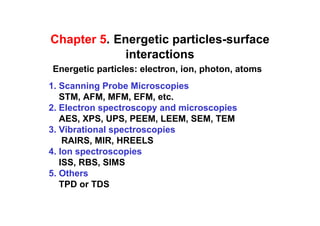
  • 1. Chapter 5. Energetic particles-surface interactions Energetic particles: electron, ion, photon, atoms 1. Scanning Probe Microscopies STM, AFM, MFM, EFM, etc. 2. Electron spectroscopy and microscopies AES, XPS, UPS, PEEM, LEEM, SEM, TEM 3. Vibrational spectroscopies RAIRS, MIR, HREELS 4. Ion spectroscopies ISS, RBS, SIMS 5. Others TPD or TDS
  • 2. Tools for Characterization Tools for Characterization • Structural analysis: SEM, TEM, XRD, SAM, SPM, PEEM, LEEM, STXM, SXPEM • Chemical analysis: AES, XPS, TPD, SIMS, EDX, SPM • Electronic, optical analysis: UV/VIS, UPS, SPM • Magnetic analysis: SQUID, SMOKE, SEMPA, SPM • Vibrational analysis: IR, HREELS, Raman, SPM • Local physico-chemical probe: SPM e, hv, ion tip e, hv, ion
  • 3. Scientific issues in nanotechnologies (Nanotech.Res. Directions: IWGN report,1999) • Fundamental properties of isolated nanostructures • Fundamental properties of ensemble of isolated nanostructures • Assemblies of nanoscale building blocks • Evaluation of concepts for devices and systems • Nanomanufacturing • Connecting nanoscience and biology • Molecular electronics Local probes with nm spatial resolution for characterization
  • 4. Scanning Probe Microcopy • Scanning Tunneling Microscopy(STM): topography, local DOS • Atomic Force Microscopy (AFM): topography, force measurement • Lateral Force Microscopy (LFM): friction • Magnetic Force Microscopy (MFM): magnetism • Electrostatic Force Microscopy (EFM): charge distribution • Nearfield Scanning Optical Microscopy (NSOM): optical properties • Scanning Capacitance Microscopy (SCM): dielectric constant, doping • Scanning Thermal Microscopy (SThM): temperature • Ballistic Electron Emission Microscopy (BEEM): interface structure • Spin-polarized STM (SP-STM): spin structure • Scanning Electro-chemical Microscopy (SECM): electrochmistry • Scanning Tunneling Potentiometry (SPM): potential surface • Photon Emission STM (PESTM): chemical identification
  • 5. References of SPM 1. P.Hansma, J. Tersoff, J. App. Phys. 61, R1 (1987) 2. Y. Kuk, P.J. Silvermann, Rev. Sci. Inst. 60, 165 (1989) 3. Scanning Tunneling Microscopy and related methods edited by R.J. Behm, N. Garcia, and H. Rohrer (1990) 4. C.J. Chen, Introduction to scanning tunneling spectroscpy (oxford, 1993) 5. H-J Gudtherodt and R. Wiesendanger(ed.), Scanning tunneling microscopy I,II,III (Springer,1991-1993) 6. J.A. Kuby and J.J. Boland, Surf. Sci. Rep. 26, 61 (1996) 7. R.J. Hamers, Scanning Probe Microscopy in Chemistry, J. Phys. Chem.100, 13013 (1996) 8. G.S. McCarty and P.S.Weiss, Scanning Probe Studies of Single Nanostructures, Chem. Rev. 99, 1983 (1999) 9. C. Bai, Scanning tunneling spectroscopy and its applications (Springer, 2000) 10. PSIA, www.psia.co.kr/appnotes/apps.htm 11. ThermoMicroscope, www.thermomicro.com/spmguide/contents. 12. Digital Instrument, www.di.com/app_notes/full_appnotes.htm 13. H.-Y. Nie, publish.uwo.ca/~hnie/mmo/all.html
  • 6. Interactions used for Imaging in SPM (a) Tunneling I~exp(kd) (d) Capacitance C(d) ~ 1/d (b) Forces (e) Thermal gradient F(d) ~ various (f) Ion flow f(d) ? (c) Optical near fields E ~1/d4 Resolution limits •The property probed •The probe size
  • 7. Comparision of Microscopes 106 SEM OM Vertical scale (A) TEM 104 102 1 STM 1 102 104 106 Lateral scale (A)
  • 8. Characteristics of Microscopies OM SEM/TEM SPM Operation air,liquid vacuum air,liquid,UHV Depth of field small large medium Lateral resolution 1 µm 1-5nm:SEM 2-10nm: AFM 0.1nm:TEM 0.1nm: STM Vertical resolution N/A N/A 0.1nm: AFM 0.01nm: STM Magnification 1X-2x103X 10X-106X 5x102X- 108X Sample not completely un-chargeable surface height transparent vacuum <10 mm compatible thin film: TEM Contrast absorption scattering tunneling reflection diffraction
  • 9. Limits of Resolution • HM (High Resolution Optical Microscope) diffraction limit ~ 150 nm • PCM (Phase Contrast Microscope) subwave length 배율 가능 • X-ray Microscope λ ∼1Α; Synchrotron radiation and X-ray optics • SEM (Scanning Electron Microscopy) Focused e-beam size > 3nm • TEM (Transmission Electron Microscopy) ~1 A; 얇은 박막시료 • LEEM (Low Electron Emission Microscopy) low energy e-beam; 20nm • PEEM (Photoemission electron Microscopy) lateral resolution~100nm; chemical analysis • FIM (Field Ion Microscopy) tip 형태 시료
  • 10. Interaction of Electrons with Sample When 20 KV e-beam is used for Ni(Z=28). • Auger electron :10-30A • Secondary electron: 100A • Backscattering electron : 1-2 µm • X-ray ~ 5 µm • Penetrated electron: 5 µm Atomic Number Interaction Accelerating voltage Volume Incidence angle
  • 11. Principle: Scanning Electron Microscopy (SEM) •Beam size: a few – 30 A •Beam Voltage: 20-40kV •Resolution: 10-100 A •Magnification: 20x-650,000x •Imaging radiations: Secondary electrons, backscattering electrons •Topographic contrast: Inclination effect, shadowing, edge contrast, E-gun •Composition contrast: backscattering yield ~ bulk composition Lens Detectors •Detections: Secondary - Secondary electrons: topography electron - Backsactering electrons: atomic # and topography Sample - X-ray fluorescence: composition http://super.gsnu.ac.kr/lecture/microscopy/em.html
  • 13. Principle: Transmission Electron Microscopy (TEM) •Beam size: a few – 30 A •Beam Voltage: 40kV- 1MV E-gun •Resolution: 1-2A Condenser •Imaging radiations: transmitted electrons, lens •Imaging contrast: Scattering effect Thin •Magnification: 60x-15,000,000x sample •Image Contrast: Objective 1) Amplitude (scattering) contrast lens - transmitted beam only (bright field image) - diffraction beam only (dark field image) Projector lens 2) Phase (interference) contrast - combination of transmitted and diffraction Screen beam - multi-beam lattice image: atomic resolution (HRTEM)
  • 14. Example: TEM images of Co-nanoparticles 60 nm Self-assembled Self-assembled 2D-monolayer 2D-monolayer Surface Modification A A Co nanoparticles B 평균 지름 = 7.8 ±1 nm B Self-assembled Self-assembled 3D-multilayer 3D-multilayer From J.I. Park and J. Cheon
  • 15. Scanning Tunneling Microscope Coarse positioning device Scanning Modes: Piezo tube scanner 1. Constant current X,Y,Z 2. Constant height Tip Current Feedback Computer Sample amplifier controller Sample bias voltage Real space imaging with atomic resolution
  • 16. Theory of STM J. Tersoff and D.R. Hamann, Phys. Rev. lett. 50, 1988 (1983) Figure From J. Wintterlin - + ψsample ψtip Ef eVbias Ef d It ~ ∑ |ψtip|2 |ψsample|2 e-2κd ~ ∑ |ψsample|2 δ(E-Ef) for low voltage limit; a point tip Constant current STM image corresponds to a surface of constant state density.
  • 17. Tunneling probability and tunneling current From Y. Kuk, W-tip Au(100)-5x20
  • 18. Charge density and Potential energy contour of Tip facing the surface S. Ciriaci, Phys. Rev. B 42, 7618 (1990)
  • 19. Bias polarity : probing filled and empty states - + ψsample ψtip Occupied state (HOMO) Ef Ef d Unoccupied state (LUMO) Ef Ef d J.J.Boland, Adv. Phys. 42, 129(1993) + -
  • 20. Tunneling Spectroscopy d: fixed It ~ ∑ ρ tip (E) ρ sample (E-eV)T(E,V) dE A (Z)IV- x,y : Topography di/dV~ ρsample (E): LDOS d2i/dV2: local vibrational spectra Si(111)-2x1 Si Ni Theory I vs V (di/dV)/(I/V) vs V J. A. Stroscio et al. Phys. Rev. Lett. 57, 2579 (1986)
  • 21. STS spectra: Si(111)-7x7 and NH3 /Si(111) Wolkow and Avouris, Phys. Rev. Lett, 60, 1049 (1988)
  • 22. Current Imaging Tunneling Spectrscopy (CITS) -Take I/V curve at each pixel of a topographic image -Take dI/dV at the fixed bias voltage Vb = -0.15 ~ 0.6 V Dangling bonds in faulted half of unit cell (adatoms) Vb = -0.6 ~ -1.0 V Faulted unfaulted Dangling bonds in second layer of atoms (rest atoms) Vb = -1.6 ~ -2.0 V Si-Si back-bonds Empty(+2 V) filled ( -2V) Topographic images
  • 23. Instrumentation C.J. Chen, Introduction to scanning tunneling spectroscpy (oxford, 1993) Tip -W tip : electrochemically etched -Pt-Ir tip: cutting Positioning -fine positioning piezoelectric ceramic (Pb(Zr,Ti)O3) eg: PZT5H d33=5.93A/V, d31 = -2.74 A/V From S.J. Garett δl = d31Vl/(OD-ID), δr = d33V x,y: 0.1A z: 0,01 A resolution -coarse positioning louse, step motor, inch worm Vibration isolation -spring, viton O-ring, air table -eddy current damping Thermal stability -smaller and simpler, better stability -symmetric component -matching the thermal coefficient
  • 24. Tip preparation -Electrochemical etching in 2N NaOH solution -Ex situ : Vacuum annealing; Field emission; Ion sputtering -In situ: high field(>-7V) scanning, controlled collision From W. Ho group
  • 25. Vibration isolation Y. Kuk, P.J. Silvermann, Rev. Sci. Inst. 60, 165 (1989) -needs ~0.01A or less (atomic corrugation ~0.1A) -Dapmed spring : fres =0.5 Hz -Vition stacks :fres = 10~100 Hz -Air tables Damping transfer function Ts Ts = (ν/νn’)2/[(1- (ν/νn’)2)2+ (ν/Q’νn’)2]1/2 νn’ : the resonance frequency Q’: the quality factor of the tip-sample junction Rigid STM assembly Vib. amplitude>1A Add isolation table Vib. amplitude <0.01 A Internal spring and air table Vib. amplitude<0.001 A
  • 26. Electronics -set the tip voltage (0-10V) and measure tunneling current (0.001~10nA) -tip-sample separation: 2-5 A, gap resistanace : 107~1010 Ω -scan x,y voltage: 1nm ~1000nm
  • 27. UHV STM From Burleigh Instrument Inc.
  • 28. Applications of STM • Surface geometry • Molecular structure • Local electronic structure • Local spin structure • Single molecular vibration • Electronic transport • Nano-fabrication • Atom manipulation • Nano-chemical reaction
  • 29. Surface Structure Various Reconstructions of Ge(100)-2x1 p(2x2) Buckled 2x1 p(2x2) 2x1 c(4x2) c(4x2) J.Y. Maeng et al (2001)
  • 30. Si(100) and Ge(100) 2x1 surface Si(001) at 80 K Clean Surface Structure Lattice Dimer Tilt π - π* Buckled- Constant Length Angle Symmetric Si(100) 5.43 Å 2.32 Å 70 0.66 eV 25 meV Ge(100 5.658 Å 2.41 Å 140 1.11 eV 60 meV )
  • 32. Molecular Adsorption: 2+2 cycloaddition reaction Fabrication of molecularly ordered organic films Anisotropic optical and electrical properties A Possible way to orient molecular devices R.J. Hamers et al, J. Phys. Chem., 101, 1489 (1997)
  • 33. Adsorption structure: Pyridine on Ge(100) tunneling through space and through bond bias dependence Vbias = -1.0 V Clean Ge Pyridine Dimer LUMO Image of π∗ bonds Substrate Ef Dimer HOMO Vbias = -1.8 V π bonds Image of It ~ ∑ |ψsample|2 δ(E-Ef) Substrate + Pyridine Ef Vbias = -2.4V Vbias = -2.4 V Ef Image of Py/Ge W-Tip Pyridine Organic molecules reduce DOS near EF, but increase DOS at lower energy.
  • 34. Possible Adsorption States of Pyridine on Si(100) Lewis base-acid reaction Lewis base-acid reaction -δ +δ [4+2] cycloaddition [4+2] cycloaddition Lu et al. New. J. Chem. 26. 160 (2002)
  • 35. Comparison of Theoretical STM Images with Experiment θ = 0.25 ML: experiment c(4x2) model theory θ = 0.5 ML: experiment p(2x2) model theory
  • 36. Long chain molecules on surface Left A 3nm x 3nm image of docosanol taken at the liquid- solid interface on graphite. The black bar is superimposed over one molecular length, measured to be 3.0 + 0.2nm. The left-hand trough (marked in the image) signifies the alcohol group, which show up slightly darker relative to the rest of the hydrocarbon chain. The individual bright Leanna C. Giancarlo, Hongbin Fang, Luis (yellow) spots along the molecular axis depict individual Avila, Leonard W. Fine, hydrogen atoms. You can actually count them and get 22 and George W. Flynn, J. Chem. Ed., 77, hydrogens per molecule (only one hydrogen per carbon is 66-71 (2000) visible to the STM since the second hydrogen on each carbon is pointing down into the graphite and therefore not seen in the image).
  • 37. STM of Metal phthalocyanines: Fe(II) d6 Ni(II) d8 Figure 3 Top view STM images of a 0.4 nm thick layer of NiPc and of 0.3 nm of FePc on Au(111) obtained with a W tip. Both samples Figure 2 Schematic orbital energy diagram for had MPc layers that had once been exposed to air. The gray scale several transition metal phthalocyanine extends over 0.3 nm. For NiPc the sample bias was +0.50 V and the complexes. In the case of iron(II), a single orbital tunneling current was 300 pA. For FePc the sample bias was +0.10 configuration cannot be used to describe the V and the tunneling current was 1.6 nA. The image was Fourier ground state, and at least two configurations are filtered to reduce noise. required. This situation is represented diagramatically by use of a broken × to indicate partial occupation of an orbital by an electron, while a full × represents near complete Xing Lu and K. W. Hipps, occupation by a single electron. This diagram is J. Phys. Chem. B, 101 (27), 5391 -5396, 1997 based on ref 1, 3, 30, and 31.
  • 38. In-situ Monitoring of Self-assembly Self-directed growth of Nanostructures Wolkow et al, Nature, 406, 48 (2000)
  • 39. Single Molecule Vibrational Spectroscopy Inelastic electron tunneling spectroscopy (IETS) hv/e I V dI/dV V dI2/dV2 V Vibration excitation of the molecule occurs when tunneling electrons have enough energy to excite a quantized vibrational level Inelastic tunneling channel B.C. Stipe. et. al., Science 280, 1732 (1998)
  • 40. Atomic Manipulation by STM -high electric field: polarize the molecule and make it jump from the surface to the tip vice versa. Iron on Copper (111): -van der Waals force between the tip and the atom use to drag the atom - Circular corral (radius=71.3A) 48 Fe atoms - Quantum-mechanical interference patterns M.F. Crommie, C.P. Lutz, D.M. Eigler. Science 262, 218-220 (1993).
  • 41. Single-Bond Formation by STM H.J. Lee and W. Ho, Science, 286, 1719(1999)
  • 42. Real Space Imaging of Two-Dimensional Antiferromagnetism On the Atomic Scale Weisendanger et al, Science 288, 1805 (2000) Nonmagnetic W tip Magnetic W tip
  • 43. Conductance : Landauer formula µ2 eVmol eV µ1 µ2 µ1 I = (2e/h)∫dE T(E,V) [f(E-µ1)-f(E- µ2)] •F(E): Fermi function •T(E,V): transmission function molecular energy levels and their coupling to the metallic contacts µ1, µ2 : electrochemical potentials µ1= Ef- eVmol µ2 =Ef+eV- eVmol W. Tian et al, J. Chem. Phys. 109, 2874(1998)
  • 44. Conductance of molecular wire: STM •Tip bias voltage = 1V, •Tunnling current = 10 pA L. A. Bumm et al , Science 271, 1705 (1996).
  • 45. Electronic Properties of Carbon Nanotubes Constant LDOS Metallic SWNT Semiconducting SWNT
  • 46. STM Topograph of Quantum Dot Ge pyramid containing ~2000 Ge atoms on Si(100) Ge dome grown by PVD on a 600 C Si(100) R.S. Williams et al, Acc. Chem. Res. 32, 425 (1999)
  • 47. STM Images of Ni Clusters at Different Sample Bias Voltages
  • 48. STS and STM of Self-assembled Co-nanoparticles Tip on self-assembled monolayer Tip on a Co nanoparticle I vs V dI/dV vs V Pileni et al, Appl. Surf. Sci. 162/163, 519 (2000)
  • 49. Tunneling Spectroscopy of InAs QD STM T=4.2K Optical d = 32A S-like P-like Ec=0.11 eV: single electron charging energy U. Banin et al, Nature, Eg=1.02 eV: nanocrystal band gap 400, 926 (2000)
  • 50. Interactions between Sample and Tip in Force Microscopy vdW force magnetic or adhesion elastic and attractive electrostatic bonding plastic properties ionic repulsion forces friction forces f Contact van der Waals force Intermitant contact r f(r) ~ -1/r6 +1/r12 total force on sample ~ 10-7 ~10-11 N Noncontact
  • 51. Force vs. Distance f r Vacuum touching untouch Air Capillary Pull off force Slope: elastic modulus of soft Contamnated sample or force constant k of in air cantilever
  • 52. Atomic Force Microscope (AFM) •Sample: conductor, nonconductor, etc •Force sensor: cantilever •Deflection detection - photodiode interferometry (10-4A) - STM
  • 53. Mode of Operation Force of interaction Contact strong (repulsive): constant force or constant distance Noncontact weak(attractive): vibrating probe Intermittent contact strong(repulsive): vibrating probe Lateral force frictional forces exert a torque on the scanning cantilever Magnetic force the magnetic field of the surface Thermal scanning the distribution of thermal conductivity
  • 54. Force Sensor: Cantilever •Material: Si , Si3N4 •Shape: pyramidal, conical tip •Typical Dimension: 100-200 µm 1-4 µm 10 µm •Stiffness - soft: contact mode ∼20nm - stiff: vibrating (dynamic force) mode •Spring constant (k): 0.1-10N/m (atom-atom k ~10N/m) •Resonance frequency: 10~100kHz eg: f = (/2π)(k/m)1/2 From DI m=1µg, k=0.1 N/m, f=100kHZ
  • 55. Nanotube tip Review: www.psia.co.kr/kr - attaching with glue - in situ CVD grwoth (a) AFM image of 2 nm tall, 10 mm wide, and 100 nm spaced silicon-oxide H.Dai et al, Nature 384, 174 (1996) (light) lines fabricated by a nanotube tip. Bias voltage = – 9 V; speed = 10 APL 73, 1508 (1998) m/s; cantilever amplitude during lithography = 0.55 nm; cantilever amplitude = 9.6 nm. (b) Silicon oxide ``words'' written by the nanotube tip.
  • 56. Image Artifacts •Tip imaging •Feedback artifacts •Convolution with other physics •Imaging processing How to check ? •Repeat the scan •Change the direction •Change the scan size •Rotate the sample •Change the scan speed AFM image of random noise. Left image is raw data. Right image is a false image, produced by applying a narrow bandpass filter to the raw data www.psia.co.kr/appnotes/apps.htm
  • 57. Scanning Modes of AFM Contact Noncontact Vibrating (tapping) •Cantilever soft hard hard •Force 1-10nN 0.1-0.01nN •Friction large small small •Distance <0.2nm ~ 1nm >10nm •Damage large small small •Surface hard surface soft or elastic surface Polymer latex particle on mica From Digital Instrument
  • 58. Vibrating Cantilever (tapping) Mode •Vibration of cantilever around its resonance frequency •Change of frequency (fo) due to interaction between sample and cantilever Resonance Frequency keff = k0 - dF/dz feff = 2π(keff /m)1/2 •Amplitude imaging •Phase imaging •Removal of lateral force contribution
  • 60. Applications of SPM • Surface morphology, especially for insulators • Lateral, adhesion, molecular and magnetic forces • Temperature, capacitance, and surface potential mapping • Nano-lithography • Surface modification and manipulation • Imaging of biomolecules, and polymers
  • 61. Atomic resolution AFM AFM (contact mode): AFM (non-contact mode): Au(111) polycrystalline film Atomic resolution on Si(111)7x7 on a glass substrate From Omicron Inc.
  • 62. STM and AFM Images of Co-Nanoparticles STM: on H/Si(111) AFM: on HOPG TEM: on Carbon grid Co-nanoparticle stripes prepared By Mirco Contact Printing AFM image UHV-STM image (200 nm x 200 nm) after annealing under 500 °C S.S.Bae et al (2001)
  • 63. Applications to biological system DNA and RNA analysis; Protein-nucleic acid complexes; Chromosomes; Cellular membranes; Proteins and peptides; Molecular crystals; Polymers and biomaterials; Ligand- receptor binding. Bio-samples have been investigated on lysine-coated glass and mica substrate, and in buffer solution. By using phase imaging technique one can distinguish the different components of the cell membranes.
  • 64. Force Measurement of DNA strands Baselt et al, J. Vac. Sci. Tech. B14, 789 (1996)
  • 65. Manipulation of Nanoparticles by AFM Ref 15 in G.S. McCarth and P.S.Weiss, Chem. Rev. 99, 1983 (1999)
  • 66. Dip pen nanolithography using AFM C. Mirkin et al, Science 283, 661 Read Prof I. Choi, lecture note (spring 2002) (1999); 295, 1702 (2002) Figure 1. AFM images and height profiles of lysozyme nanoarrays. (A) Lateral force image of an 8 µm by 8 µm square lattice of MHA dots deposited onto an Au substrate. The array was imaged with an uncoated tip at 42% relative humidity (scan rate = 4 Hz). (B) Topography image (contact mode) and height profile of the nanoarray after lysozyme adsorption. A tip-substrate contact force of 0.2 nN was used to avoid damaging the protein patterns with the tip. (C) A tapping mode image (silicon cantilever, spring contant = ~40 N/m) and height profile of a hexagonal lysozyme nanoarray. The image was taken at a scan rate of 0.5 Hz to obtain high resolution. (D) Three-dimensional topographic image of a lysozyme nanoarray, consisting of a line grid and dots with intentionally varied feature dimensions. Imaging was done in contact mode as described in (B).
  • 67. Conductive AFM Conductive AFM is used for collecting simultaneous topography imaging and current imaging. Specifically, standard conductive AFM operates in contact AFM mode. Variations in surface conductivity can be distinguished using this mode. Conductive AFM operates in contact AFM mode by using a conductive AFM tip. The contact tip is scanned in contact with the sample surface. Just like contact AFM, the Z feedback loop uses the DC cantilever deflection signal to maintain a constant force between the tip and the sample to generate the topography image. At the same time, a DC bias is applied to the tip. The sample is held at ground potential. The built-in pre- amplifier in the scanner head measures the current passing through the tip and sample. http://www.thermomicro.com/spmguide/1-5-0.htm#NANO
  • 68. AFM/STM lithography resist의 표면 topography에도 매우 민감합니다. 대부분 E- beam resist는 주입된 전자 수에 민감하므로 전압에 의하여 제어보다 전류를 집적 제어하는 것이 보다 재현성 있는 패턴 을 얻을 수 있습니다. 따라서 AFM과 STM를 결합하여 resist 표면을 일정한 거리와 힘를 유지하도록 하면서resist 막의 두 께가 변화더라도 전류를 일정하게 유지시키도록 ( 20 pA ~ 1 nA ) 탐침의 전압을 (10~100 V) 변화 시키는 독립적인 feedback loop를 도입하였습니다.(STM mode). 두 제어 방 법을 결합하여 패턴 전체에 걸쳐 전자의 주입양(electron dose) 일정하게 유지하여 수십 nm 수준의 패튼의 재현성을 얻었을 뿐만 아니라 기존 E-beam lithography에서 발생하는 depth of focal length 문제를 해결하였습니다. From http://www.psia.co.kr/
  • 69. AFM-tip-induced Local Oxidation on Si Ph. Avouris et al, App. Phys. A 66, S659 (1998)
  • 70. Lateral Force Microscopy •Contact mode •Detect vertical and lateral twisting due to friction •Simultaneous AFM & LFM imaging •Information about friction High resolution topography (top) and Lateral Force mode (bottom) images of a commercially avail-able PET film. The silicate fillers show increased friction in the lateral force image. www.tmmicro.com/tech/modes/lfm.htm
  • 71. Force Modulation Microscopy •Contact AFM mode •Periodic signal is applied to either to tip or sample •Simultaneous imaging of topography and material properties •Amplitude change due to elastic properties of the sample PSIA, www.psia.co.kr/appnotes/apps.htm
  • 72. Phase Detection Microscopy Phase imaging is useful for differentiating between component phases of composite materials. The bulk of the wood pulp shown in this figure consists of cellulose microfibrils that are highlighted by phase imaging. In addition, a lignin component -- not apparent in From Digital Instrument the topography -- appears as areas of light contrast atop the cellulose component •Intermittant-contact AFM mode •Monitoring of phase lag between the cantilever oscillation (solid wave) relative to the piezo drive (dashed wave). •Simultaneous imaging of topography and material properties •Change in mechanical properties of sample surface
  • 73. Chemical Force Microscopy CH3 COOH (A) topography (B) friction force using a tip modified with a COOH-terminated SAM, (C) frinction force using a tip modified with a methyl-terminated SAM. Light regions in (B) and (C) indicate high friction; dark regions indicate low frinction. A. Noy et al, Ann. Rev. Mater. Sci. 27, 381 (1997)
  • 74. Magnetic Force Microscopy Glass Hard Disk Sample dF/dz =dFm/dz + dFvdw/dz, •Ferromagnetic tip: Co, Cr •Noncontact mode (>100A) AFM •vdW force: short range force image •Magnetic force: long range force small force gradient •Close imaging: topography •Distant imaging: magnetic properties MFM image http://www.tmmicro.com/tech/index.htm
  • 75. Scanning Hall Probe Microscopy z H y ++++++ RH= Ey/jxH i x -------- = -1/ne Ey F= -evxH The spots correspond to individual magnetic lines or vortices that are formed in a superconducting film of LaSrCaCuO This probe allows one to measure microscopic magnetic patterns by using a submicron Hall probe to sense local magnetic fields. Fields as low as 0.1 gauss with 0.3um spatial resolution can be achieved. It competes with magnetic force microscopy which might have superior resolution but is not calibrated and with scanning SQUID microscopy which has higher magnetic field sensitivity but poorer spatial resolution. Hans Hallen and Albert Chang. (Bell lab), Applied Physics Letters, 61, pg 1974 (1992).
  • 76. Electrostatic Force Microscopy(EFM) Scanning Kelvin Probe Microscopy (SKPM) Scanning Tunneling Potentiometry (STP) Scanning Maxwell Microscopy (SMM) Metallic tip Bias Voltage • Ferroelectric materials • Charge distribution on surfaces • Failure analysis on the device http://www.tmmicro.com/tech/index.htm
  • 77. Theory of EFM Electrostatic force between the sample and the tip (Fcapacitance = dEc /dz , Ec = CV2/2) F = Fcapacitance + F coulomb = (1/2)V2(dC/dz) + (1/4πε z2)QsQt = (1/2) (dC/dz) (Vdc+Vac cos ωt)2 - (1/4πε z2)Qs (Qs+CVdc+CVaccos ωt) = (1/2) (dC/dV) (V 2dc+ (1/2) V2ac) - (1/4πε z2)Qs (Qs+CVdc) + (2Vdc dC/dz - QsC /4πε z)Vaccos ωt + (1/4)dC/dzV2ac cos 2ωt •Ist harmonic term - Surface potential (Vdc ) - surface charge (Qs) •2nd harmonic term - dC/dz : doping concentration
  • 78. Scanning Capacitance Microscopy (SCM) Transistor Oxide Thickness Metallic tip Contact Topograph SCM • LC capacitance circuit • Doping concentration • Local dielectric constant http://www.psia.co.kr/appnotes/apps.htm
  • 79. Scanning Thermal Microscopy • Subsurface defect review • Semiconductor failure analysis • Measure conductivity differences in copolymers, surface coatings etc
  • 80. Hybrid Tools: AFM inside SEM M.F. Yu et al, Nanotechnology 10, 244 (1999)
  • 81. Nearfield Scanning Optical Microscopy Topography and Optical properties Glass hv Detector Al φ=60-200nm d Fluorescence image of •Near field: d<<λ a single DiIC molecule. •Resolution ~ d and φ Image courtesy of P. •Approach: shear force Barabara/Dan Higgins http://www.psia.co.kr/data/nsom.htm
  • 82. Scanning Electrochemical Microscopy From Prof. J. Kwak Electrochemistry Surface structure Electrochemical deposition Corrosion
  • 83. Photon Emission STM Photon detector A A FEEDBACK Local chemical environment G.S. McCarty and P.S. Weiss, Chem. Rev. 99, 1983 (1999)
  • 84. BEEM (Ballistic Electron Emission Microscopy) A Ballistic Electron A Ef gap FEEDBACK Tip Base Collector(Si) STP (Scanning Tunneling Potentiometry) A .. . . FEEDBACK
  • 85. Summary STM • real space imaging • high lateral and vertical resolution • STS probe electronic properties • sensitive to noise • image quality depends on tip conditions • not true topographic imaging • only for conductive materials AFM and others •apply to nonconducting materials : biomolecules, ceramic • real topographic imaging • probe various physical properties: magnetic, electrostatic, hydrophobicity, friction, elastic modulus, etc. • can manipulate molecules and fabricate nanostructures • low lateral resolution ~50A • contact mode can damage the sample • image distortion due to the presence of water • difficulties in chemical identification
  • 86. Future Directions for Characterization of Nanosystems • Instrument for analysis of biomolecules, and polymers • 3-D structure determination • Nanostructure chemical determination • Functional parallel probe arrays • Standardization and metrology • New nano-manipulator • Non-SPM probes that use ions or electrons • In-situ nondestructive monitoring techniques