SlideShare ist ein Scribd-Unternehmen logo
1 von 15
Downloaden Sie, um offline zu lesen
VIPer22ADIP
                ®
                                                                                                           VIPer22AS

                    LOW POWER OFF LINE SMPS PRIMARY SWITCHER
TYPICAL POWER CAPABILITY
      Mains type                    SO-8                DIP-8
       European
                                    12 W                20 W
    (195 - 265 Vac)
    US / Wide range                                                                         SO-8                  DIP-8
                                    7W                  12 W
     (85 - 265 Vac)
                                                                                                   ORDER CODES
                                                                                    PACKAGE           TUBE           T&R
n   FIXED 60 KHZ SWITCHING FREQUENCY
                                                                                SO-8               VIPer22AS   VIPer22AS13TR
n   9V TO 38V WIDE RANGE VDD VOLTAGE                                            DIP-8              VIPer22ADIP -
n   CURRENT MODE CONTROL
n   AUXILIARY UNDERVOLTAGE LOCKOUT                                         MOSFET on the same silicon chip. Typical
    WITH HYSTERESIS                                                        applications cover off line power supplies for
n HIGH VOLTAGE START UP CURRENT                                            battery charger adapters, standby power supplies
                                                                           for TV or monitors, auxiliary supplies for motor
    SOURCE                                                                 control, etc. The internal control circuit offers the
n OVERTEMPERATURE, OVERCURRENT AND                                         following benefits:
    OVERVOLTAGE PROTECTION WITH                                            – Large input voltage range on the VDD pin
    AUTORESTART                                                               accommodates changes in auxiliary supply
                                                                              voltage. This feature is well adapted to battery
DESCRIPTION                                                                   charger adapter configurations.
The VIPer22A combines a dedicated current mode                             – Automatic burst mode in low load condition.
PWM controller with a high voltage Power                                   – Overvoltage protection in hiccup mode.

BLOCK DIAGRAM

                                                                                                                    DRAIN


                                           ON/OFF
                                                                      60kHz
                          REGULATOR                                 OSCILLATOR


                           INTERNAL                                                  PWM
                                                                           S        LATCH
                            SUPPLY                  OVERTEMP.
                                                                    R1     FF   Q
                                                    DETECTOR
                                                                     R2 R3 R4


           VDD                  _                                                                    +
                                                                                     BLANKING
                      8/14.5V                                                                        _   0.23 V
                                +
                                                             OVERVOLTAGE
                                                                LATCH                                              230 Ω
                                                        R
                                +
                                                    S   FF   Q
                        42V     _

                                                                                                         1 kΩ
           FB


                                                                                                                   SOURCE


September 2002                                                                                                                 1/15
VIPer22ADIP / VIPer22AS

PIN FUNCTION
  Name                                                                       Function
            Power supply of the control circuits. Also provides a charging current during start up thanks to a high
            voltage current source connected to the drain. For this purpose, an hysteresis comparator monitors the
            VDD voltage and provides two thresholds:
   VDD      - VDDon: Voltage value (typically 14.5V) at which the device starts switching and turns off the start up
            current source.
            - VDDoff: Voltage value (typically 8V) at which the device stops switching and turns on the start up current
            source.
 SOURCE     Power MOSFET source and circuit ground reference.
            Power MOSFET drain. Also used by the internal high voltage current source during start up phase for
  DRAIN     charging the external VDD capacitor.
            Feedback input. The useful voltage range extends from 0V to 1V, and defines the peak drain MOSFET
       FB   current. The current limitation, which corresponds to the maximum drain current, is obtained for a FB pin
            shorted to the SOURCE pin.

CURRENT AND VOLTAGE CONVENTIONS


                                         I DD                                                 ID


                                                              VDD               DRAIN
                                                 I FB
                                                        FB         CONTROL
                                   VDD                                                             VD
                                                                               SOURCE
                                           VFB
                                                        VIPer22A


CONNECTION DIAGRAM


                SOURCE    1                 8    DRAIN                             SOURCE      1               8   DRAIN

                SOURCE    2                 7    DRAIN                             SOURCE      2               7   DRAIN

                     FB   3                 6    DRAIN                                   FB    3               6   DRAIN

                    VDD   4                 5    DRAIN                                  VDD    4               5   DRAIN


                               SO-8                                                                     DIP8


2/15
VIPer22ADIP / VIPer22AS

ABSOLUTE MAXIMUM RATINGS
  Symbol                                       Parameter                                                 Value                 Unit
   VDS(sw)     Switching Drain Source Voltage (Tj=25 ... 125°C)               (See note 1)             -0.3 ... 730             V
   VDS(st)     Start Up Drain Source Voltage (Tj=25 ... 125°C)                (See note 2)             -0.3 ... 400             V
      ID       Continuous Drain Current                                                            Internally limited           A
    VDD        Supply Voltage                                                                            0 ... 50               V
     IFB       Feedback Current                                                                             3                  mA
               Electrostatic Discharge:
    VESD       Machine Model (R=0Ω; C=200pF)                                                              200                    V
               Charged Device Model                                                                       1.5                   kV
      Tj       Junction Operating Temperature                                                      Internally limited           °C
      Tc       Case Operating Temperature                                                              -40 to 150               °C
     Tstg      Storage Temperature                                                                     -55 to 150               °C
Note: 1. This parameter applies when the start up current source is off. This is the case when the VDD voltage has reached VDDon and
         remains above VDDoff.
      2. This parameter applies when the start up current source is on. This is the case when the VDD voltage has not yet reached VDDon
         or has fallen below V DDoff.

THERMAL DATA
  Symbol                                       Parameter                                               Max Value               Unit
               Thermal Resistance Junction-Pins for :
 Rthj-case     SO-8                                                                                        25                 °C/W
               DIP-8                                                                                       15
               Thermal Resistance Junction-Ambient for :
  Rthj-amb     SO-8                                                           (See note 1)                 55                 °C/W
               DIP-8                                                          (See note 1)                 45
Note: 1. When mounted on a standard single-sided FR4 board with 200 mm² of Cu (at least 35 µm thick) connected to all DRAIN pins.

ELECTRICAL CHARACTERISTICS (Tj=25°C, VDD=18V, unless otherwise specified)
POWER SECTION
  Symbol               Parameter                            Test Conditions                     Min.      Typ.        Max.     Unit
   BVDSS       Drain-Source Voltage           ID=1mA; VFB=2V                                    730                             V
    IDSS       Off State Drain Current        VDS=500V; VFB=2V; Tj=125°C                                              0.1      mA
               Static Drain-Source            ID=0.4A                                                      15         17
   RDSon                                                                                                                        Ω
               On State Resistance            ID=0.4A; Tj=100°C                                                       31
                                              ID=0.2A; VIN=300V                 (See fig.1)
      tf       Fall Time                                                                                  100                   ns
                                                                              (See note 1)
                                              ID=0.4A; VIN=300V                 (See fig.1)
      tr       Rise Time                                                                                   50                   ns
                                                                              (See note 1)
    Coss       Drain Capacitance              VDS=25V                                                      40                   pF
Note: 1. On clamped inductive load


                                                                                                                                 3/15
VIPer22ADIP / VIPer22AS

ELECTRICAL CHARACTERISTICS (Tj=25°C, VDD=18V, unless otherwise specified)
SUPPLY SECTION
  Symbol                Parameter                            Test Conditions                      Min.      Typ.          Max.   Unit

    IDDch      Start Up Charging               VDS=100V; VDD=0V ...VDDon (See fig. 2)                         -1                 mA
               Current
               Start Up Charging               VDD=5V; VDS=100V
    IDDoff     Current                                                                              0                            mA
                                               Tj > TSD - THYST
               in Thermal Shutdown

    IDD0       Operating Supply Current I =2mA
                                         FB                                                                   3            5     mA
               Not Switching

    IDD1       Operating Supply Current I =0.5mA; I =50mA                            (Note 1)
                                         FB        D                                                         4.5                 mA
               Switching
    DRST       Restart Duty Cycle                                                (See fig. 3)                 16                  %
               VDD Undervoltage
   VDDoff                                                                   (See fig. 2 & 3)        7         8            9      V
               Shutdown Threshold
   VDDon       VDD Start Up Threshold                                       (See fig. 2 & 3)       13       14.5          16      V
               VDD Threshold
   VDDhyst                                                                       (See fig. 2)      5.8       6.5          7.2     V
               Hysteresis
               VDD Overvoltage
   VDDovp                                                                                          38         42          46      V
               Threshold
Note: 1. These test conditions obtained with a resistive load are leading to the maximum conduction time of the device.


OSCILLATOR SECTION
  Symbol                Parameter                            Test Conditions                      Min.      Typ.          Max.   Unit

    FOSC       Oscillator Frequency            VDD=VDDoff ... 35V; Tj=0 ... 100°C                  54         60          66     kHz
               Total Variation


PWM COMPARATOR SECTION
  Symbol                Parameter                            Test Conditions                      Min.      Typ.          Max.   Unit
       GID     IFB to ID Current Gain                                            (See fig. 4)                560
    IDlim      Peak Current Limitation         VFB=0V                            (See fig. 4)     0.56       0.7          0.84    A
    IFBsd      IFB Shutdown Current                                              (See fig. 4)                0.9                 mA
     RFB       FB Pin Input Impedance          ID=0mA                            (See fig. 4)                1.2                 kΩ

       td      Current Sense Delay to          ID=0.4A                                                       200                 ns
               Turn-Off
       tb      Blanking Time                                                                                 500                 ns
   tONmin      Minimum Turn On Time                                                                          700                 ns


OVERTEMPERATURE SECTION
  Symbol                Parameter                            Test Conditions                      Min.      Typ.          Max.   Unit

       TSD     Thermal Shutdown
                                                                                 (See fig. 5)     140        170                 °C
               Temperature

   THYST       Thermal Shutdown
                                                                                 (See fig. 5)                 40                 °C
               Hysteresis


4/15
VIPer22ADIP / VIPer22AS

Figure 1 : Rise and Fall Time
      ID


                                                                                                                      C         L    D
                                                                                                     C << Coss


                                                                        t

   VDS
                                                                                               VDD                    DRAIN

                                                                                         FB         CONTROL                                      300V
     90%
                                                                                                                 SOURCE
                       tfv                                        trv
                                                                                         VIPer22A


    10%                                                                 t


Figure 2 : Start Up VDD Current
    IDD

     IDD0


            VDDhyst


                                                                        VDD
              VDDoff                 VDDon

    IDDch
                                               VDS = 100 V
                                               Fsw = 0 kHz


Figure 3 : Restart Duty Cycle


    VDD
   VDDon

                                                                                                                          VDD            DRAIN

   VDDoff                                                                         10µF                           FB        CONTROL                      100V

                                    tCH                          tST                                                                 SOURCE
                                                                              t                          2V
                                                                                                                 VIPer22A
                                              tST
                             D RST = -------------------------
                                     t ST + tCH


                                                                                                                                                           5/15
VIPer22ADIP / VIPer22AS

Figure 4 : Peak Drain Current vs. Feedback Current


                                                                                                                               100V

         ID                                                                                                             4mH


       IDpeak


                   1/FOSC                                                                                  VDD         DRAIN

                                                                                                   FB
                                                         t        18V                                       CONTROL                   100V


                                                                                                                      SOURCE
                                                                              IFB        47nF       VIPer22A


                                                 VFB

                                     FBsd ⋅ FB
                                 I         R


       The drain current limitation is
       obtained for VFB = 0 V, and a
       negative current is drawn from
       the FB pin. See the Application                                                                      IFB
       section for further details.


                                                 IDpeak
                                                                          ∆I Dpea k
                                                      IDlim       GID = – ----------------------
                                                                                               -
                                                                               ∆I FB


                                                                                                            IFB
                                                  0                                                IFBsd


Figure 5 : Thermal Shutdown
         Tj
        TSD
                             THYST


                                                              t

       VDD


   VDDon                                Automatic
                                         start up


                                                              t


6/15
VIPer22ADIP / VIPer22AS

Figure 6 : Switching Frequency vs Temperature


                                                     1.01

                                                                                Vdd = 10V ... 35V

                                                        1
                     Normalized Frequency


                                                     0.99


                                                     0.98


                                                     0.97
                                                            -20   0   20     40       60       80   100   120
                                                                           Temperature (°C)


Figure 7 : Current Limitation vs Temperature


                                                     1.04
                                                     1.03
                     Normalized Current Limitation


                                                     1.02
                                                     1.01
                                                        1
                                                     0.99
                                                     0.98
                                                                                       Vin = 100V
                                                     0.97
                                                                                       Vdd = 20V
                                                     0.96
                                                     0.95
                                                     0.94
                                                            -20   0   20      40      60       80   100   120
                                                                           Temperature (°C)


                                                                                                                         7/15
VIPer22ADIP / VIPer22AS

Figure 8 : Rectangular U-I output characteristics for battery charger


                                                                                                                                       DCOUT
                                                                          R1                                  T1             C1
                                                                                    C2                                  D2
                                                                                                D1


                                                                                    D3
                    T2
         F1
 AC IN         C3
                                D4               ISO1
                            +


                                                               U1
                                     C4
                                                                    VDD                      DRAIN
                            -


                                                           FB
                                          C5                         CONTROL


                                                     C6                              SOURCE
                                                               VIPerX2A

                                                                                                                   C7


                                                                    R2


                                                                                                     D5


                                                                               U2
                                                                     R3                       Vcc                       R4
                                                                                         Vref


                                                          R5                                                                      R6
                                                                     C8                                                 C9
                                                                                         -                +
                                               C10
                                                                                         +                -

                                                                                         GND
                                                          R7         R8                                                           R9
                                                                               TSM101

                                                          R10
                                                                                                                                       GND


RECTANGULAR U-I OUTPUT                                     WIDE RANGE OF VDD VOLTAGE
CHARACTERISTIC                                             The VDD pin voltage range extends from 9V to 38V.
A complete regulation scheme can achieve                   This feature offers a great flexibility in design to
combined and accurate output characteristics.              achieve various behaviors. In figure 8 a forward
Figure 8 presents a secondary feedback through             configuration has been chosen to supply the
an optocoupler driven by a TSM101. This device             device with two benefits:
offers two operational amplifiers and a voltage            – as soon as the device starts switching, it
reference, thus allowing the regulation of both              immediately receives some energy from the
output voltage and current. An integrated OR                 auxiliary winding. C5 can be therefore reduced
function performs the combination of the two                 and a small ceramic chip (100 nF) is sufficient to
resulting error signals, leading to a dual voltage           insure the filtering function. The total start up
and current limitation, known as a rectangular               time from the switch on of input voltage to output
output characteristic.                                       voltage presence is dramatically decreased.
This type of power supply is especially useful for         – the output current characteristic can be
battery chargers where the output is mainly used in          maintained even with very low or zero output
current mode, in order to deliver a defined charging         voltage. Since the TSM101 is also supplied in
rate. The accurate voltage regulation is also                forward mode, it keeps the current regulation up
convenient for Li-ion batteries which require both           whatever the output voltage is.The VDD pin
modes of operation.                                          voltage may vary as much as the input voltage,
                                                             that is to say with a ratio of about 4 for a wide
                                                             range application.


8/15
VIPer22ADIP / VIPer22AS

FEEDBACK PIN PRINCIPLE OF OPERATION                                       In a real application, the FB pin is driven with an
A feedback pin controls the operation of the                              optocoupler as shown on figure 9 which acts as a
device. Unlike conventional PWM control circuits                          pull up. So, it is not possible to really short this pin
which use a voltage input (the inverted input of an                       to ground and the above drain current value is not
operational amplifier), the FB pin is sensitive to                        achievable. Nevertheless, the capacitor C is
current. Figure 9 presents the internal current                           averaging the voltage on the FB pin, and when the
mode structure.                                                           optocoupler is off (start up or short circuit), it can be
                                                                          assumed that the corresponding voltage is very
The Power MOSFET delivers a sense current Is                              close to 0 V.
which is proportional to the main current Id. R2
receives this current and the current coming from                         For low drain currents, the formula (1) is valid as
the FB pin. The voltage across R2 is then                                 long as IFB satisfies IFB< IFBsd, where IFBsd is an
compared to a fixed reference voltage of about                            internal threshold of the VIPer22A. If IFB exceeds
0.23 V. The MOSFET is switched off when the                               this threshold the device will stop switching. This is
following equation is reached:                                            represented on figure 4, and IFBsd value is
R 2 ⋅ ( IS + IFB ) = 0.23V                                                specified in the PWM COMPARATOR SECTION.
                                                                          Actually, as soon as the drain current is about 12%
By extracting IS:                                                         of Idlim, that is to say 85 mA, the device will enter
      0.23V                                                               a burst mode operation by missing switching
I S = ------------- – I FB
                  -                                                       cycles. This is especially important when the
          R2
                                                                          converter is lightly loaded.
Using the current sense ratio of the MOSFET GID :
                                                                          It is then possible to build the total DC transfer
I D = G ID ⋅ IS = G ID ⋅  ------------- – IFB
                           0.23V                                          function between ID and IFB as shown on figure 10.
                                       -
                          R2                                            This figure also takes into account the internal
The current limitation is obtained with the FB pin                        blanking time and its associated minimum turn on
shorted to ground (VFB = 0 V). This leads to a                            time. This imposes a minimum drain current under
negative current sourced by this pin, and                                 which the device is no more able to control it in a
expressed by:                                                             linear way. This drain current depends on the
                                                                          primary inductance value of the transformer and
        0.23V                                                             the input voltage. Two cases may occur,
IFB = – -------------
                    -
            R1                                                            depending on the value of this current versus the
By reporting this expression in the previous one, it                      fixed 85 mA value, as described above.
is possible to obtain the drain current limitation
                                                                          START UP SEQUENCE
IDlim:
                                                                          This device includes a high voltage start up current
IDlim = G ID ⋅ 0.23V ⋅  ----- + ----- 
                           1       1
                             -       -                                    source connected on the drain of the device. As
                        R 2 R 1                                         soon as a voltage is applied on the input of the
                                                                          converter, this start up current source is activated
Figure 9 : Internal Current Control Structure                             as long as VDD is lower than VDDon. When
                                                                          reaching VDDon, the start up current source is
                                                                 DRAIN
                                                                          switched off and the device begins to operate by
                                                60kHz                Id
                                                                          turning on and off its main power MOSFET. As the
                                              OSCILLATOR
                                                                          FB pin does not receive any current from the
                                                                          optocoupler, the device operates at full current
                    +Vdd                          S
                                                PWM
                                                       Q
                                                                          capacity and the output voltage rises until reaching
                                               LATCH
                                                  R
                                                                          Figure 10 : IFB Transfer function
   Secondary
   feedback
                                                                                                         IDpeak
                                      0.23V                 Is
                           IFB                                                                                         IDlim
                                       1 kΩ
                                 FB
                                         R1

                           C                  230 Ω    R2

                                                                                                                                      Part masked by the
                                                                                                           1                              IFBsd threshold
                                                                              t                     ⋅V
                                                                                ONmin                          IN
                                                                 SOURCE       --------------------------------------
                                                                                                                   -
                                                                                                L
                                                                                                  85mA
                                                                                                           2
                                                                              t                     ⋅V
                                                                                ONmin                          IN
                                                                              --------------------------------------
                                                                                                                   -                                 IFB
                                                                                                L
                                                                                                                  0                  IFBsd


                                                                                                                                                            9/15
VIPer22ADIP / VIPer22AS

Figure 11 : Start Up Sequence                            Figure 12 : Overvoltage Sequence

   VDD                                                       VDD
   VDDon                                                    VDDovp


   VDDoff                                                    VDDon

                             tss                             VDDoff
                                                                                                          t
                                                   t

        IFB                                                  VDS


                                                   t                                                      t

  VOUT
                                                         OVERVOLTAGE THRESHOLD
                                                         An overvoltage detector on the VDD pin allows the
                                                         VIPer22A to reset itself when VDD exceeds
                                                         VDDovp. This is illustrated in figure 12, which shows
                                                         the whole sequence of an overvoltage event. Note
                                                   t
                                                         that this event is only latched for the time needed
                                                         by VDD to reach VDDoff, and then the device
                                                         resumes normal operation automatically.
the regulation point where the secondary loop
begins to send a current in the optocoupler. At this
point, the converter enters a regulated operation
where the FB pin receives the amount of current
needed to deliver the right power on secondary
side.
This sequence is shown in figure 11. Note that
during the real starting phase tss, the device
consumes some energy from the VDD capacitor,
waiting for the auxiliary winding to provide a
continuous supply. If the value of this capacitor is
too low, the start up phase is terminated before
receiving any energy from the auxiliary winding
and the converter never starts up. This is illustrated
also in the same figure in dashed lines.


10/15
VIPer22ADIP / VIPer22AS


              SO-8 MECHANICAL DATA

              mm.                                    inch
DIM.
       MIN.   TYP     MAX.               MIN.        TYP.       MAX.
 A                    1.75                                      0.068
a1     0.1            0.25               0.003                  0.009
a2                    1.65                                      0.064
a3     0.65           0.85               0.025                  0.033
 b     0.35           0.48               0.013                  0.018
b1     0.19           0.25               0.007                  0.010
 C     0.25            0.5               0.010                  0.019
c1                           45 (typ.)
 D     4.8             5                 0.188                  0.196
 E     5.8             6.2               0.228                  0.244
 e            1.27                                   0.050
e3            3.81                                   0.150
 F     3.8             4                 0.14                   0.157
 L     0.4            1.27               0.015                  0.050
 M                     0.6                                      0.023
 S                           8 (max.)
L1     0.8             1.2               0.031                  0.047


                                                                        11/15


                                                                            1
VIPer22ADIP / VIPer22AS


                         Plastic DIP-8 MECHANICAL DATA
                                           mm.
             DIM.
                             MIN.          TYP                  MAX.
              A                                                 5.33
             A1              0.38
             A2              2.92          3.30                 4.95
              b              0.36          0.46                 0.56
             b2              1.14          1.52                 1.78
              c              0.20          0.25                 0.36
              D              9.02          9.27                 10.16
              E              7.62          7.87                 8.26
             E1              6.10          6.35                 7.11
              e                            2.54
             eA                            7.62
             eB                                                 10.92
              L              2.92          3.30                 3.81
        Package Weight                    Gr. 470


                                                         P001


12/15
VIPer22ADIP / VIPer22AS

                                     SO-8 TUBE SHIPMENT (no suffix)


                       B
                                                 C             Base Q.ty                                    100
                                                               Bulk Q.ty                                   2000
                                                               Tube length (± 0.5)                          532
                                                 A             A                                            3.2
                                                               B                                             6
                                                               C (± 0.1)                                    0.6

                                                              All dimensions are in mm.

                               TAPE AND REEL SHIPMENT (suffix “13TR”)

                                                                                  REEL DIMENSIONS
                                                                                   Base Q.ty                2500
                                                                                   Bulk Q.ty                2500
                                                                                   A (max)                  330
                                                                                   B (min)                   1.5
                                                                                   C (± 0.2)                 13
                                                                                   F                        20.2
                                                                                   G (+ 2 / -0)             12.4
                                                                                   N (min)                   60
                                                                                   T (max)                  18.4

                                                                                  All dimensions are in mm.


TAPE DIMENSIONS
According to Electronic Industries Association
(EIA) Standard 481 rev. A, Feb 1986
 Tape width                     W         12
 Tape Hole Spacing         P0 (± 0.1)      4
 Component Spacing              P          8
 Hole Diameter             D (± 0.1/-0)   1.5
 Hole Diameter              D1 (min)      1.5
 Hole Position              F (± 0.05)    5.5
 Compartment Depth           K (max)      4.5
 Hole Spacing              P1 (± 0.1)      2

All dimensions are in mm.                               End


                                                                                                                                  Start

                                                     Top          No components         Components                No components
                                                     cover
                                                     tape        500mm min
                                                                              Empty components pockets        500mm min
                                                                              saled with cover tape.

                                                                                  User direction of feed


                                                                                                                                    13/15

                                                                                                                                          1
VIPer22ADIP / VIPer22AS


                          DIP-8 TUBE SHIPMENT (no suffix)


                  A            C
                                          Base Q.ty                   20
                                          Bulk Q.ty                  1000
                                          Tube length (± 0.5)         532
                                          A                           8.4
                               B          B                          11.2
                                          C (± 0.1)                   0.8

                                         All dimensions are in mm.


14/15

                                                                            1
VIPer22ADIP / VIPer22AS


Information furnished is believed to be accurate and reliable. However, STMicroelectronics assumes no responsibility for the consequences
of use of such information nor for any infringement of patents or other rights of third parties which may results from its use. No license is
granted by implication or otherwise under any patent or patent rights of STMicroelectronics. Specifications mentioned in this publication are
subject to change without notice. This publication supersedes and replaces all information previously supplied. STMicroelectronics products
are not authorized for use as critical components in life support devices or systems without express written approval of STMicroelectronics.
                                             The ST logo is a trademark of STMicroelectronics

                                    © 2002 STMicroelectronics - Printed in ITALY- All Rights Reserved.

                                                STMicroelectronics GROUP OF COMPANIES
          Australia - Brazil - Canada - China - Finland - France - Germany - Hong Kong - India - Israel - Italy - Japan - Malaysia -
                          Malta - Morocco - Singapore - Spain - Sweden - Switzerland - United Kingdom - U.S.A.

                                                            http://www.st.com


                                                                                                                                       15/15

Weitere ähnliche Inhalte

Was ist angesagt?

Amplificador tda7057 aq
Amplificador tda7057 aqAmplificador tda7057 aq
Amplificador tda7057 aqAntonio Gil
 
Mc 33078n op amp dual lo noise
Mc 33078n op amp dual lo noiseMc 33078n op amp dual lo noise
Mc 33078n op amp dual lo noisevakumtube
 
MUSES8920の英語のデータシート
MUSES8920の英語のデータシートMUSES8920の英語のデータシート
MUSES8920の英語のデータシートspicepark
 
Datavideo PD-3
Datavideo PD-3Datavideo PD-3
Datavideo PD-3AVNed
 
ELECTRICAL PROJECT ABSTRACT-Embedded pic microcontroller based motor protecti...
ELECTRICAL PROJECT ABSTRACT-Embedded pic microcontroller based motor protecti...ELECTRICAL PROJECT ABSTRACT-Embedded pic microcontroller based motor protecti...
ELECTRICAL PROJECT ABSTRACT-Embedded pic microcontroller based motor protecti...ASHOKKUMAR RAMAR
 
Valve & Amplifier Design, EL34 (6CA7) Data, Mullard Valves
Valve & Amplifier Design, EL34 (6CA7) Data, Mullard ValvesValve & Amplifier Design, EL34 (6CA7) Data, Mullard Valves
Valve & Amplifier Design, EL34 (6CA7) Data, Mullard ValvesValve Data
 
M62502FPのデータシート
M62502FPのデータシートM62502FPのデータシート
M62502FPのデータシートTsuyoshi Horigome
 
Reducing Electrical Control Panel Size
Reducing Electrical Control Panel SizeReducing Electrical Control Panel Size
Reducing Electrical Control Panel SizeCMA/Flodyne/Hydradyne
 
74ls283datasheet
74ls283datasheet74ls283datasheet
74ls283datasheetneghy
 
LM2575 Voltage Regulator Datasheet
LM2575 Voltage Regulator DatasheetLM2575 Voltage Regulator Datasheet
LM2575 Voltage Regulator DatasheetYong Heui Cho
 
Acx502 bmu
Acx502 bmuAcx502 bmu
Acx502 bmuUjwal Ks
 

Was ist angesagt? (20)

Amplificador tda7057 aq
Amplificador tda7057 aqAmplificador tda7057 aq
Amplificador tda7057 aq
 
Mc 33078n op amp dual lo noise
Mc 33078n op amp dual lo noiseMc 33078n op amp dual lo noise
Mc 33078n op amp dual lo noise
 
MUSES8920の英語のデータシート
MUSES8920の英語のデータシートMUSES8920の英語のデータシート
MUSES8920の英語のデータシート
 
Datavideo PD-3
Datavideo PD-3Datavideo PD-3
Datavideo PD-3
 
Ed ch 9 power
Ed ch 9 powerEd ch 9 power
Ed ch 9 power
 
Cd4093 bc
Cd4093 bcCd4093 bc
Cd4093 bc
 
An 1072
An 1072An 1072
An 1072
 
Adi jul1311
Adi jul1311Adi jul1311
Adi jul1311
 
ELECTRICAL PROJECT ABSTRACT-Embedded pic microcontroller based motor protecti...
ELECTRICAL PROJECT ABSTRACT-Embedded pic microcontroller based motor protecti...ELECTRICAL PROJECT ABSTRACT-Embedded pic microcontroller based motor protecti...
ELECTRICAL PROJECT ABSTRACT-Embedded pic microcontroller based motor protecti...
 
Valve & Amplifier Design, EL34 (6CA7) Data, Mullard Valves
Valve & Amplifier Design, EL34 (6CA7) Data, Mullard ValvesValve & Amplifier Design, EL34 (6CA7) Data, Mullard Valves
Valve & Amplifier Design, EL34 (6CA7) Data, Mullard Valves
 
M62502FPのデータシート
M62502FPのデータシートM62502FPのデータシート
M62502FPのデータシート
 
Reducing Electrical Control Panel Size
Reducing Electrical Control Panel SizeReducing Electrical Control Panel Size
Reducing Electrical Control Panel Size
 
Mean well d-30 dual out
Mean well   d-30 dual outMean well   d-30 dual out
Mean well d-30 dual out
 
Pdiusbd11
Pdiusbd11Pdiusbd11
Pdiusbd11
 
74ls283datasheet
74ls283datasheet74ls283datasheet
74ls283datasheet
 
Td1410
Td1410Td1410
Td1410
 
LM2575 Voltage Regulator Datasheet
LM2575 Voltage Regulator DatasheetLM2575 Voltage Regulator Datasheet
LM2575 Voltage Regulator Datasheet
 
Lpc662
Lpc662Lpc662
Lpc662
 
DS25CP102 (English)
DS25CP102 (English)DS25CP102 (English)
DS25CP102 (English)
 
Acx502 bmu
Acx502 bmuAcx502 bmu
Acx502 bmu
 

Ähnlich wie Vip Er22a

Original High Performance Off-Line Controller IC ACT30 CT30 30 New Active-Semi
Original High Performance Off-Line Controller IC ACT30 CT30 30 New Active-SemiOriginal High Performance Off-Line Controller IC ACT30 CT30 30 New Active-Semi
Original High Performance Off-Line Controller IC ACT30 CT30 30 New Active-SemiAUTHELECTRONIC
 
Original Power Supply IC LNK626PG LNK626P LNK626 DIP-7 New Power Integration
Original Power Supply IC LNK626PG LNK626P LNK626 DIP-7 New Power IntegrationOriginal Power Supply IC LNK626PG LNK626P LNK626 DIP-7 New Power Integration
Original Power Supply IC LNK626PG LNK626P LNK626 DIP-7 New Power IntegrationAUTHELECTRONIC
 
An9611
An9611An9611
An9611anfeco
 
Design and fabrication of over voltage relay
Design and fabrication of over voltage relay Design and fabrication of over voltage relay
Design and fabrication of over voltage relay Prem Kumar
 
Master thesis presentation
Master thesis presentationMaster thesis presentation
Master thesis presentationMayur Sarode
 
Webinar: Desmistificando projetos de fontes chaveadas
Webinar: Desmistificando projetos de fontes chaveadasWebinar: Desmistificando projetos de fontes chaveadas
Webinar: Desmistificando projetos de fontes chaveadasEmbarcados
 
電流臨界モード方式PFC制御回路の解説書
電流臨界モード方式PFC制御回路の解説書電流臨界モード方式PFC制御回路の解説書
電流臨界モード方式PFC制御回路の解説書Tsuyoshi Horigome
 
FL7701 APEC Demo Performance_SMappus 01192012
FL7701 APEC Demo Performance_SMappus 01192012FL7701 APEC Demo Performance_SMappus 01192012
FL7701 APEC Demo Performance_SMappus 01192012Steve Mappus
 
Advanced motion controls sr30a40ac
Advanced motion controls sr30a40acAdvanced motion controls sr30a40ac
Advanced motion controls sr30a40acElectromate
 

Ähnlich wie Vip Er22a (20)

5 l0380r
5 l0380r5 l0380r
5 l0380r
 
Original High Performance Off-Line Controller IC ACT30 CT30 30 New Active-Semi
Original High Performance Off-Line Controller IC ACT30 CT30 30 New Active-SemiOriginal High Performance Off-Line Controller IC ACT30 CT30 30 New Active-Semi
Original High Performance Off-Line Controller IC ACT30 CT30 30 New Active-Semi
 
Ad598
Ad598Ad598
Ad598
 
Lsa47.2
Lsa47.2Lsa47.2
Lsa47.2
 
Lsa47.2
Lsa47.2Lsa47.2
Lsa47.2
 
Original Power Supply IC LNK626PG LNK626P LNK626 DIP-7 New Power Integration
Original Power Supply IC LNK626PG LNK626P LNK626 DIP-7 New Power IntegrationOriginal Power Supply IC LNK626PG LNK626P LNK626 DIP-7 New Power Integration
Original Power Supply IC LNK626PG LNK626P LNK626 DIP-7 New Power Integration
 
An9611
An9611An9611
An9611
 
Design and fabrication of over voltage relay
Design and fabrication of over voltage relay Design and fabrication of over voltage relay
Design and fabrication of over voltage relay
 
Mean welll rs-35
Mean welll   rs-35Mean welll   rs-35
Mean welll rs-35
 
Si1029X
Si1029XSi1029X
Si1029X
 
Mean well rs-25
Mean well   rs-25Mean well   rs-25
Mean well rs-25
 
Master thesis presentation
Master thesis presentationMaster thesis presentation
Master thesis presentation
 
raimon ribal
raimon ribalraimon ribal
raimon ribal
 
Lm567
Lm567Lm567
Lm567
 
Webinar: Desmistificando projetos de fontes chaveadas
Webinar: Desmistificando projetos de fontes chaveadasWebinar: Desmistificando projetos de fontes chaveadas
Webinar: Desmistificando projetos de fontes chaveadas
 
tca785
tca785tca785
tca785
 
電流臨界モード方式PFC制御回路の解説書
電流臨界モード方式PFC制御回路の解説書電流臨界モード方式PFC制御回路の解説書
電流臨界モード方式PFC制御回路の解説書
 
FL7701 APEC Demo Performance_SMappus 01192012
FL7701 APEC Demo Performance_SMappus 01192012FL7701 APEC Demo Performance_SMappus 01192012
FL7701 APEC Demo Performance_SMappus 01192012
 
22 series relays
22 series relays22 series relays
22 series relays
 
Advanced motion controls sr30a40ac
Advanced motion controls sr30a40acAdvanced motion controls sr30a40ac
Advanced motion controls sr30a40ac
 

Kürzlich hochgeladen

Cash Payment 9602870969 Escort Service in Udaipur Call Girls
Cash Payment 9602870969 Escort Service in Udaipur Call GirlsCash Payment 9602870969 Escort Service in Udaipur Call Girls
Cash Payment 9602870969 Escort Service in Udaipur Call GirlsApsara Of India
 
Monthly Social Media Update April 2024 pptx.pptx
Monthly Social Media Update April 2024 pptx.pptxMonthly Social Media Update April 2024 pptx.pptx
Monthly Social Media Update April 2024 pptx.pptxAndy Lambert
 
Pharma Works Profile of Karan Communications
Pharma Works Profile of Karan CommunicationsPharma Works Profile of Karan Communications
Pharma Works Profile of Karan Communicationskarancommunications
 
Tech Startup Growth Hacking 101 - Basics on Growth Marketing
Tech Startup Growth Hacking 101  - Basics on Growth MarketingTech Startup Growth Hacking 101  - Basics on Growth Marketing
Tech Startup Growth Hacking 101 - Basics on Growth MarketingShawn Pang
 
RE Capital's Visionary Leadership under Newman Leech
RE Capital's Visionary Leadership under Newman LeechRE Capital's Visionary Leadership under Newman Leech
RE Capital's Visionary Leadership under Newman LeechNewman George Leech
 
7.pdf This presentation captures many uses and the significance of the number...
7.pdf This presentation captures many uses and the significance of the number...7.pdf This presentation captures many uses and the significance of the number...
7.pdf This presentation captures many uses and the significance of the number...Paul Menig
 
Call Girls In Panjim North Goa 9971646499 Genuine Service
Call Girls In Panjim North Goa 9971646499 Genuine ServiceCall Girls In Panjim North Goa 9971646499 Genuine Service
Call Girls In Panjim North Goa 9971646499 Genuine Serviceritikaroy0888
 
M.C Lodges -- Guest House in Jhang.
M.C Lodges --  Guest House in Jhang.M.C Lodges --  Guest House in Jhang.
M.C Lodges -- Guest House in Jhang.Aaiza Hassan
 
VIP Call Girls In Saharaganj ( Lucknow ) 🔝 8923113531 🔝 Cash Payment (COD) 👒
VIP Call Girls In Saharaganj ( Lucknow  ) 🔝 8923113531 🔝  Cash Payment (COD) 👒VIP Call Girls In Saharaganj ( Lucknow  ) 🔝 8923113531 🔝  Cash Payment (COD) 👒
VIP Call Girls In Saharaganj ( Lucknow ) 🔝 8923113531 🔝 Cash Payment (COD) 👒anilsa9823
 
Grateful 7 speech thanking everyone that has helped.pdf
Grateful 7 speech thanking everyone that has helped.pdfGrateful 7 speech thanking everyone that has helped.pdf
Grateful 7 speech thanking everyone that has helped.pdfPaul Menig
 
Russian Faridabad Call Girls(Badarpur) : ☎ 8168257667, @4999
Russian Faridabad Call Girls(Badarpur) : ☎ 8168257667, @4999Russian Faridabad Call Girls(Badarpur) : ☎ 8168257667, @4999
Russian Faridabad Call Girls(Badarpur) : ☎ 8168257667, @4999Tina Ji
 
Vip Dewas Call Girls #9907093804 Contact Number Escorts Service Dewas
Vip Dewas Call Girls #9907093804 Contact Number Escorts Service DewasVip Dewas Call Girls #9907093804 Contact Number Escorts Service Dewas
Vip Dewas Call Girls #9907093804 Contact Number Escorts Service Dewasmakika9823
 
Ensure the security of your HCL environment by applying the Zero Trust princi...
Ensure the security of your HCL environment by applying the Zero Trust princi...Ensure the security of your HCL environment by applying the Zero Trust princi...
Ensure the security of your HCL environment by applying the Zero Trust princi...Roland Driesen
 
Best VIP Call Girls Noida Sector 40 Call Me: 8448380779
Best VIP Call Girls Noida Sector 40 Call Me: 8448380779Best VIP Call Girls Noida Sector 40 Call Me: 8448380779
Best VIP Call Girls Noida Sector 40 Call Me: 8448380779Delhi Call girls
 
Socio-economic-Impact-of-business-consumers-suppliers-and.pptx
Socio-economic-Impact-of-business-consumers-suppliers-and.pptxSocio-economic-Impact-of-business-consumers-suppliers-and.pptx
Socio-economic-Impact-of-business-consumers-suppliers-and.pptxtrishalcan8
 
Call Girls In DLf Gurgaon ➥99902@11544 ( Best price)100% Genuine Escort In 24...
Call Girls In DLf Gurgaon ➥99902@11544 ( Best price)100% Genuine Escort In 24...Call Girls In DLf Gurgaon ➥99902@11544 ( Best price)100% Genuine Escort In 24...
Call Girls In DLf Gurgaon ➥99902@11544 ( Best price)100% Genuine Escort In 24...lizamodels9
 
A DAY IN THE LIFE OF A SALESMAN / WOMAN
A DAY IN THE LIFE OF A  SALESMAN / WOMANA DAY IN THE LIFE OF A  SALESMAN / WOMAN
A DAY IN THE LIFE OF A SALESMAN / WOMANIlamathiKannappan
 
MONA 98765-12871 CALL GIRLS IN LUDHIANA LUDHIANA CALL GIRL
MONA 98765-12871 CALL GIRLS IN LUDHIANA LUDHIANA CALL GIRLMONA 98765-12871 CALL GIRLS IN LUDHIANA LUDHIANA CALL GIRL
MONA 98765-12871 CALL GIRLS IN LUDHIANA LUDHIANA CALL GIRLSeo
 

Kürzlich hochgeladen (20)

Best Practices for Implementing an External Recruiting Partnership
Best Practices for Implementing an External Recruiting PartnershipBest Practices for Implementing an External Recruiting Partnership
Best Practices for Implementing an External Recruiting Partnership
 
Cash Payment 9602870969 Escort Service in Udaipur Call Girls
Cash Payment 9602870969 Escort Service in Udaipur Call GirlsCash Payment 9602870969 Escort Service in Udaipur Call Girls
Cash Payment 9602870969 Escort Service in Udaipur Call Girls
 
Monthly Social Media Update April 2024 pptx.pptx
Monthly Social Media Update April 2024 pptx.pptxMonthly Social Media Update April 2024 pptx.pptx
Monthly Social Media Update April 2024 pptx.pptx
 
Pharma Works Profile of Karan Communications
Pharma Works Profile of Karan CommunicationsPharma Works Profile of Karan Communications
Pharma Works Profile of Karan Communications
 
Tech Startup Growth Hacking 101 - Basics on Growth Marketing
Tech Startup Growth Hacking 101  - Basics on Growth MarketingTech Startup Growth Hacking 101  - Basics on Growth Marketing
Tech Startup Growth Hacking 101 - Basics on Growth Marketing
 
RE Capital's Visionary Leadership under Newman Leech
RE Capital's Visionary Leadership under Newman LeechRE Capital's Visionary Leadership under Newman Leech
RE Capital's Visionary Leadership under Newman Leech
 
7.pdf This presentation captures many uses and the significance of the number...
7.pdf This presentation captures many uses and the significance of the number...7.pdf This presentation captures many uses and the significance of the number...
7.pdf This presentation captures many uses and the significance of the number...
 
Call Girls In Panjim North Goa 9971646499 Genuine Service
Call Girls In Panjim North Goa 9971646499 Genuine ServiceCall Girls In Panjim North Goa 9971646499 Genuine Service
Call Girls In Panjim North Goa 9971646499 Genuine Service
 
M.C Lodges -- Guest House in Jhang.
M.C Lodges --  Guest House in Jhang.M.C Lodges --  Guest House in Jhang.
M.C Lodges -- Guest House in Jhang.
 
VIP Call Girls In Saharaganj ( Lucknow ) 🔝 8923113531 🔝 Cash Payment (COD) 👒
VIP Call Girls In Saharaganj ( Lucknow  ) 🔝 8923113531 🔝  Cash Payment (COD) 👒VIP Call Girls In Saharaganj ( Lucknow  ) 🔝 8923113531 🔝  Cash Payment (COD) 👒
VIP Call Girls In Saharaganj ( Lucknow ) 🔝 8923113531 🔝 Cash Payment (COD) 👒
 
Nepali Escort Girl Kakori \ 9548273370 Indian Call Girls Service Lucknow ₹,9517
Nepali Escort Girl Kakori \ 9548273370 Indian Call Girls Service Lucknow ₹,9517Nepali Escort Girl Kakori \ 9548273370 Indian Call Girls Service Lucknow ₹,9517
Nepali Escort Girl Kakori \ 9548273370 Indian Call Girls Service Lucknow ₹,9517
 
Grateful 7 speech thanking everyone that has helped.pdf
Grateful 7 speech thanking everyone that has helped.pdfGrateful 7 speech thanking everyone that has helped.pdf
Grateful 7 speech thanking everyone that has helped.pdf
 
Russian Faridabad Call Girls(Badarpur) : ☎ 8168257667, @4999
Russian Faridabad Call Girls(Badarpur) : ☎ 8168257667, @4999Russian Faridabad Call Girls(Badarpur) : ☎ 8168257667, @4999
Russian Faridabad Call Girls(Badarpur) : ☎ 8168257667, @4999
 
Vip Dewas Call Girls #9907093804 Contact Number Escorts Service Dewas
Vip Dewas Call Girls #9907093804 Contact Number Escorts Service DewasVip Dewas Call Girls #9907093804 Contact Number Escorts Service Dewas
Vip Dewas Call Girls #9907093804 Contact Number Escorts Service Dewas
 
Ensure the security of your HCL environment by applying the Zero Trust princi...
Ensure the security of your HCL environment by applying the Zero Trust princi...Ensure the security of your HCL environment by applying the Zero Trust princi...
Ensure the security of your HCL environment by applying the Zero Trust princi...
 
Best VIP Call Girls Noida Sector 40 Call Me: 8448380779
Best VIP Call Girls Noida Sector 40 Call Me: 8448380779Best VIP Call Girls Noida Sector 40 Call Me: 8448380779
Best VIP Call Girls Noida Sector 40 Call Me: 8448380779
 
Socio-economic-Impact-of-business-consumers-suppliers-and.pptx
Socio-economic-Impact-of-business-consumers-suppliers-and.pptxSocio-economic-Impact-of-business-consumers-suppliers-and.pptx
Socio-economic-Impact-of-business-consumers-suppliers-and.pptx
 
Call Girls In DLf Gurgaon ➥99902@11544 ( Best price)100% Genuine Escort In 24...
Call Girls In DLf Gurgaon ➥99902@11544 ( Best price)100% Genuine Escort In 24...Call Girls In DLf Gurgaon ➥99902@11544 ( Best price)100% Genuine Escort In 24...
Call Girls In DLf Gurgaon ➥99902@11544 ( Best price)100% Genuine Escort In 24...
 
A DAY IN THE LIFE OF A SALESMAN / WOMAN
A DAY IN THE LIFE OF A  SALESMAN / WOMANA DAY IN THE LIFE OF A  SALESMAN / WOMAN
A DAY IN THE LIFE OF A SALESMAN / WOMAN
 
MONA 98765-12871 CALL GIRLS IN LUDHIANA LUDHIANA CALL GIRL
MONA 98765-12871 CALL GIRLS IN LUDHIANA LUDHIANA CALL GIRLMONA 98765-12871 CALL GIRLS IN LUDHIANA LUDHIANA CALL GIRL
MONA 98765-12871 CALL GIRLS IN LUDHIANA LUDHIANA CALL GIRL
 

Vip Er22a

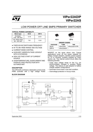
  • 1. VIPer22ADIP ® VIPer22AS LOW POWER OFF LINE SMPS PRIMARY SWITCHER TYPICAL POWER CAPABILITY Mains type SO-8 DIP-8 European 12 W 20 W (195 - 265 Vac) US / Wide range SO-8 DIP-8 7W 12 W (85 - 265 Vac) ORDER CODES PACKAGE TUBE T&R n FIXED 60 KHZ SWITCHING FREQUENCY SO-8 VIPer22AS VIPer22AS13TR n 9V TO 38V WIDE RANGE VDD VOLTAGE DIP-8 VIPer22ADIP - n CURRENT MODE CONTROL n AUXILIARY UNDERVOLTAGE LOCKOUT MOSFET on the same silicon chip. Typical WITH HYSTERESIS applications cover off line power supplies for n HIGH VOLTAGE START UP CURRENT battery charger adapters, standby power supplies for TV or monitors, auxiliary supplies for motor SOURCE control, etc. The internal control circuit offers the n OVERTEMPERATURE, OVERCURRENT AND following benefits: OVERVOLTAGE PROTECTION WITH – Large input voltage range on the VDD pin AUTORESTART accommodates changes in auxiliary supply voltage. This feature is well adapted to battery DESCRIPTION charger adapter configurations. The VIPer22A combines a dedicated current mode – Automatic burst mode in low load condition. PWM controller with a high voltage Power – Overvoltage protection in hiccup mode. BLOCK DIAGRAM DRAIN ON/OFF 60kHz REGULATOR OSCILLATOR INTERNAL PWM S LATCH SUPPLY OVERTEMP. R1 FF Q DETECTOR R2 R3 R4 VDD _ + BLANKING 8/14.5V _ 0.23 V + OVERVOLTAGE LATCH 230 Ω R + S FF Q 42V _ 1 kΩ FB SOURCE September 2002 1/15
  • 2. VIPer22ADIP / VIPer22AS PIN FUNCTION Name Function Power supply of the control circuits. Also provides a charging current during start up thanks to a high voltage current source connected to the drain. For this purpose, an hysteresis comparator monitors the VDD voltage and provides two thresholds: VDD - VDDon: Voltage value (typically 14.5V) at which the device starts switching and turns off the start up current source. - VDDoff: Voltage value (typically 8V) at which the device stops switching and turns on the start up current source. SOURCE Power MOSFET source and circuit ground reference. Power MOSFET drain. Also used by the internal high voltage current source during start up phase for DRAIN charging the external VDD capacitor. Feedback input. The useful voltage range extends from 0V to 1V, and defines the peak drain MOSFET FB current. The current limitation, which corresponds to the maximum drain current, is obtained for a FB pin shorted to the SOURCE pin. CURRENT AND VOLTAGE CONVENTIONS I DD ID VDD DRAIN I FB FB CONTROL VDD VD SOURCE VFB VIPer22A CONNECTION DIAGRAM SOURCE 1 8 DRAIN SOURCE 1 8 DRAIN SOURCE 2 7 DRAIN SOURCE 2 7 DRAIN FB 3 6 DRAIN FB 3 6 DRAIN VDD 4 5 DRAIN VDD 4 5 DRAIN SO-8 DIP8 2/15
  • 3. VIPer22ADIP / VIPer22AS ABSOLUTE MAXIMUM RATINGS Symbol Parameter Value Unit VDS(sw) Switching Drain Source Voltage (Tj=25 ... 125°C) (See note 1) -0.3 ... 730 V VDS(st) Start Up Drain Source Voltage (Tj=25 ... 125°C) (See note 2) -0.3 ... 400 V ID Continuous Drain Current Internally limited A VDD Supply Voltage 0 ... 50 V IFB Feedback Current 3 mA Electrostatic Discharge: VESD Machine Model (R=0Ω; C=200pF) 200 V Charged Device Model 1.5 kV Tj Junction Operating Temperature Internally limited °C Tc Case Operating Temperature -40 to 150 °C Tstg Storage Temperature -55 to 150 °C Note: 1. This parameter applies when the start up current source is off. This is the case when the VDD voltage has reached VDDon and remains above VDDoff. 2. This parameter applies when the start up current source is on. This is the case when the VDD voltage has not yet reached VDDon or has fallen below V DDoff. THERMAL DATA Symbol Parameter Max Value Unit Thermal Resistance Junction-Pins for : Rthj-case SO-8 25 °C/W DIP-8 15 Thermal Resistance Junction-Ambient for : Rthj-amb SO-8 (See note 1) 55 °C/W DIP-8 (See note 1) 45 Note: 1. When mounted on a standard single-sided FR4 board with 200 mm² of Cu (at least 35 µm thick) connected to all DRAIN pins. ELECTRICAL CHARACTERISTICS (Tj=25°C, VDD=18V, unless otherwise specified) POWER SECTION Symbol Parameter Test Conditions Min. Typ. Max. Unit BVDSS Drain-Source Voltage ID=1mA; VFB=2V 730 V IDSS Off State Drain Current VDS=500V; VFB=2V; Tj=125°C 0.1 mA Static Drain-Source ID=0.4A 15 17 RDSon Ω On State Resistance ID=0.4A; Tj=100°C 31 ID=0.2A; VIN=300V (See fig.1) tf Fall Time 100 ns (See note 1) ID=0.4A; VIN=300V (See fig.1) tr Rise Time 50 ns (See note 1) Coss Drain Capacitance VDS=25V 40 pF Note: 1. On clamped inductive load 3/15
  • 4. VIPer22ADIP / VIPer22AS ELECTRICAL CHARACTERISTICS (Tj=25°C, VDD=18V, unless otherwise specified) SUPPLY SECTION Symbol Parameter Test Conditions Min. Typ. Max. Unit IDDch Start Up Charging VDS=100V; VDD=0V ...VDDon (See fig. 2) -1 mA Current Start Up Charging VDD=5V; VDS=100V IDDoff Current 0 mA Tj > TSD - THYST in Thermal Shutdown IDD0 Operating Supply Current I =2mA FB 3 5 mA Not Switching IDD1 Operating Supply Current I =0.5mA; I =50mA (Note 1) FB D 4.5 mA Switching DRST Restart Duty Cycle (See fig. 3) 16 % VDD Undervoltage VDDoff (See fig. 2 & 3) 7 8 9 V Shutdown Threshold VDDon VDD Start Up Threshold (See fig. 2 & 3) 13 14.5 16 V VDD Threshold VDDhyst (See fig. 2) 5.8 6.5 7.2 V Hysteresis VDD Overvoltage VDDovp 38 42 46 V Threshold Note: 1. These test conditions obtained with a resistive load are leading to the maximum conduction time of the device. OSCILLATOR SECTION Symbol Parameter Test Conditions Min. Typ. Max. Unit FOSC Oscillator Frequency VDD=VDDoff ... 35V; Tj=0 ... 100°C 54 60 66 kHz Total Variation PWM COMPARATOR SECTION Symbol Parameter Test Conditions Min. Typ. Max. Unit GID IFB to ID Current Gain (See fig. 4) 560 IDlim Peak Current Limitation VFB=0V (See fig. 4) 0.56 0.7 0.84 A IFBsd IFB Shutdown Current (See fig. 4) 0.9 mA RFB FB Pin Input Impedance ID=0mA (See fig. 4) 1.2 kΩ td Current Sense Delay to ID=0.4A 200 ns Turn-Off tb Blanking Time 500 ns tONmin Minimum Turn On Time 700 ns OVERTEMPERATURE SECTION Symbol Parameter Test Conditions Min. Typ. Max. Unit TSD Thermal Shutdown (See fig. 5) 140 170 °C Temperature THYST Thermal Shutdown (See fig. 5) 40 °C Hysteresis 4/15
  • 5. VIPer22ADIP / VIPer22AS Figure 1 : Rise and Fall Time ID C L D C << Coss t VDS VDD DRAIN FB CONTROL 300V 90% SOURCE tfv trv VIPer22A 10% t Figure 2 : Start Up VDD Current IDD IDD0 VDDhyst VDD VDDoff VDDon IDDch VDS = 100 V Fsw = 0 kHz Figure 3 : Restart Duty Cycle VDD VDDon VDD DRAIN VDDoff 10µF FB CONTROL 100V tCH tST SOURCE t 2V VIPer22A tST D RST = ------------------------- t ST + tCH 5/15
  • 6. VIPer22ADIP / VIPer22AS Figure 4 : Peak Drain Current vs. Feedback Current 100V ID 4mH IDpeak 1/FOSC VDD DRAIN FB t 18V CONTROL 100V SOURCE IFB 47nF VIPer22A VFB FBsd ⋅ FB I R The drain current limitation is obtained for VFB = 0 V, and a negative current is drawn from the FB pin. See the Application IFB section for further details. IDpeak ∆I Dpea k IDlim GID = – ---------------------- - ∆I FB IFB 0 IFBsd Figure 5 : Thermal Shutdown Tj TSD THYST t VDD VDDon Automatic start up t 6/15
  • 7. VIPer22ADIP / VIPer22AS Figure 6 : Switching Frequency vs Temperature 1.01 Vdd = 10V ... 35V 1 Normalized Frequency 0.99 0.98 0.97 -20 0 20 40 60 80 100 120 Temperature (°C) Figure 7 : Current Limitation vs Temperature 1.04 1.03 Normalized Current Limitation 1.02 1.01 1 0.99 0.98 Vin = 100V 0.97 Vdd = 20V 0.96 0.95 0.94 -20 0 20 40 60 80 100 120 Temperature (°C) 7/15
  • 8. VIPer22ADIP / VIPer22AS Figure 8 : Rectangular U-I output characteristics for battery charger DCOUT R1 T1 C1 C2 D2 D1 D3 T2 F1 AC IN C3 D4 ISO1 + U1 C4 VDD DRAIN - FB C5 CONTROL C6 SOURCE VIPerX2A C7 R2 D5 U2 R3 Vcc R4 Vref R5 R6 C8 C9 - + C10 + - GND R7 R8 R9 TSM101 R10 GND RECTANGULAR U-I OUTPUT WIDE RANGE OF VDD VOLTAGE CHARACTERISTIC The VDD pin voltage range extends from 9V to 38V. A complete regulation scheme can achieve This feature offers a great flexibility in design to combined and accurate output characteristics. achieve various behaviors. In figure 8 a forward Figure 8 presents a secondary feedback through configuration has been chosen to supply the an optocoupler driven by a TSM101. This device device with two benefits: offers two operational amplifiers and a voltage – as soon as the device starts switching, it reference, thus allowing the regulation of both immediately receives some energy from the output voltage and current. An integrated OR auxiliary winding. C5 can be therefore reduced function performs the combination of the two and a small ceramic chip (100 nF) is sufficient to resulting error signals, leading to a dual voltage insure the filtering function. The total start up and current limitation, known as a rectangular time from the switch on of input voltage to output output characteristic. voltage presence is dramatically decreased. This type of power supply is especially useful for – the output current characteristic can be battery chargers where the output is mainly used in maintained even with very low or zero output current mode, in order to deliver a defined charging voltage. Since the TSM101 is also supplied in rate. The accurate voltage regulation is also forward mode, it keeps the current regulation up convenient for Li-ion batteries which require both whatever the output voltage is.The VDD pin modes of operation. voltage may vary as much as the input voltage, that is to say with a ratio of about 4 for a wide range application. 8/15
  • 9. VIPer22ADIP / VIPer22AS FEEDBACK PIN PRINCIPLE OF OPERATION In a real application, the FB pin is driven with an A feedback pin controls the operation of the optocoupler as shown on figure 9 which acts as a device. Unlike conventional PWM control circuits pull up. So, it is not possible to really short this pin which use a voltage input (the inverted input of an to ground and the above drain current value is not operational amplifier), the FB pin is sensitive to achievable. Nevertheless, the capacitor C is current. Figure 9 presents the internal current averaging the voltage on the FB pin, and when the mode structure. optocoupler is off (start up or short circuit), it can be assumed that the corresponding voltage is very The Power MOSFET delivers a sense current Is close to 0 V. which is proportional to the main current Id. R2 receives this current and the current coming from For low drain currents, the formula (1) is valid as the FB pin. The voltage across R2 is then long as IFB satisfies IFB< IFBsd, where IFBsd is an compared to a fixed reference voltage of about internal threshold of the VIPer22A. If IFB exceeds 0.23 V. The MOSFET is switched off when the this threshold the device will stop switching. This is following equation is reached: represented on figure 4, and IFBsd value is R 2 ⋅ ( IS + IFB ) = 0.23V specified in the PWM COMPARATOR SECTION. Actually, as soon as the drain current is about 12% By extracting IS: of Idlim, that is to say 85 mA, the device will enter 0.23V a burst mode operation by missing switching I S = ------------- – I FB - cycles. This is especially important when the R2 converter is lightly loaded. Using the current sense ratio of the MOSFET GID : It is then possible to build the total DC transfer I D = G ID ⋅ IS = G ID ⋅  ------------- – IFB 0.23V function between ID and IFB as shown on figure 10. -  R2  This figure also takes into account the internal The current limitation is obtained with the FB pin blanking time and its associated minimum turn on shorted to ground (VFB = 0 V). This leads to a time. This imposes a minimum drain current under negative current sourced by this pin, and which the device is no more able to control it in a expressed by: linear way. This drain current depends on the primary inductance value of the transformer and 0.23V the input voltage. Two cases may occur, IFB = – ------------- - R1 depending on the value of this current versus the By reporting this expression in the previous one, it fixed 85 mA value, as described above. is possible to obtain the drain current limitation START UP SEQUENCE IDlim: This device includes a high voltage start up current IDlim = G ID ⋅ 0.23V ⋅  ----- + -----  1 1 - - source connected on the drain of the device. As  R 2 R 1 soon as a voltage is applied on the input of the converter, this start up current source is activated Figure 9 : Internal Current Control Structure as long as VDD is lower than VDDon. When reaching VDDon, the start up current source is DRAIN switched off and the device begins to operate by 60kHz Id turning on and off its main power MOSFET. As the OSCILLATOR FB pin does not receive any current from the optocoupler, the device operates at full current +Vdd S PWM Q capacity and the output voltage rises until reaching LATCH R Figure 10 : IFB Transfer function Secondary feedback IDpeak 0.23V Is IFB IDlim 1 kΩ FB R1 C 230 Ω R2 Part masked by the 1 IFBsd threshold t ⋅V ONmin IN SOURCE -------------------------------------- - L 85mA 2 t ⋅V ONmin IN -------------------------------------- - IFB L 0 IFBsd 9/15
  • 10. VIPer22ADIP / VIPer22AS Figure 11 : Start Up Sequence Figure 12 : Overvoltage Sequence VDD VDD VDDon VDDovp VDDoff VDDon tss VDDoff t t IFB VDS t t VOUT OVERVOLTAGE THRESHOLD An overvoltage detector on the VDD pin allows the VIPer22A to reset itself when VDD exceeds VDDovp. This is illustrated in figure 12, which shows the whole sequence of an overvoltage event. Note t that this event is only latched for the time needed by VDD to reach VDDoff, and then the device resumes normal operation automatically. the regulation point where the secondary loop begins to send a current in the optocoupler. At this point, the converter enters a regulated operation where the FB pin receives the amount of current needed to deliver the right power on secondary side. This sequence is shown in figure 11. Note that during the real starting phase tss, the device consumes some energy from the VDD capacitor, waiting for the auxiliary winding to provide a continuous supply. If the value of this capacitor is too low, the start up phase is terminated before receiving any energy from the auxiliary winding and the converter never starts up. This is illustrated also in the same figure in dashed lines. 10/15
  • 11. VIPer22ADIP / VIPer22AS SO-8 MECHANICAL DATA mm. inch DIM. MIN. TYP MAX. MIN. TYP. MAX. A 1.75 0.068 a1 0.1 0.25 0.003 0.009 a2 1.65 0.064 a3 0.65 0.85 0.025 0.033 b 0.35 0.48 0.013 0.018 b1 0.19 0.25 0.007 0.010 C 0.25 0.5 0.010 0.019 c1 45 (typ.) D 4.8 5 0.188 0.196 E 5.8 6.2 0.228 0.244 e 1.27 0.050 e3 3.81 0.150 F 3.8 4 0.14 0.157 L 0.4 1.27 0.015 0.050 M 0.6 0.023 S 8 (max.) L1 0.8 1.2 0.031 0.047 11/15 1
  • 12. VIPer22ADIP / VIPer22AS Plastic DIP-8 MECHANICAL DATA mm. DIM. MIN. TYP MAX. A 5.33 A1 0.38 A2 2.92 3.30 4.95 b 0.36 0.46 0.56 b2 1.14 1.52 1.78 c 0.20 0.25 0.36 D 9.02 9.27 10.16 E 7.62 7.87 8.26 E1 6.10 6.35 7.11 e 2.54 eA 7.62 eB 10.92 L 2.92 3.30 3.81 Package Weight Gr. 470 P001 12/15
  • 13. VIPer22ADIP / VIPer22AS SO-8 TUBE SHIPMENT (no suffix) B C Base Q.ty 100 Bulk Q.ty 2000 Tube length (± 0.5) 532 A A 3.2 B 6 C (± 0.1) 0.6 All dimensions are in mm. TAPE AND REEL SHIPMENT (suffix “13TR”) REEL DIMENSIONS Base Q.ty 2500 Bulk Q.ty 2500 A (max) 330 B (min) 1.5 C (± 0.2) 13 F 20.2 G (+ 2 / -0) 12.4 N (min) 60 T (max) 18.4 All dimensions are in mm. TAPE DIMENSIONS According to Electronic Industries Association (EIA) Standard 481 rev. A, Feb 1986 Tape width W 12 Tape Hole Spacing P0 (± 0.1) 4 Component Spacing P 8 Hole Diameter D (± 0.1/-0) 1.5 Hole Diameter D1 (min) 1.5 Hole Position F (± 0.05) 5.5 Compartment Depth K (max) 4.5 Hole Spacing P1 (± 0.1) 2 All dimensions are in mm. End Start Top No components Components No components cover tape 500mm min Empty components pockets 500mm min saled with cover tape. User direction of feed 13/15 1
  • 14. VIPer22ADIP / VIPer22AS DIP-8 TUBE SHIPMENT (no suffix) A C Base Q.ty 20 Bulk Q.ty 1000 Tube length (± 0.5) 532 A 8.4 B B 11.2 C (± 0.1) 0.8 All dimensions are in mm. 14/15 1
  • 15. VIPer22ADIP / VIPer22AS Information furnished is believed to be accurate and reliable. However, STMicroelectronics assumes no responsibility for the consequences of use of such information nor for any infringement of patents or other rights of third parties which may results from its use. No license is granted by implication or otherwise under any patent or patent rights of STMicroelectronics. Specifications mentioned in this publication are subject to change without notice. This publication supersedes and replaces all information previously supplied. STMicroelectronics products are not authorized for use as critical components in life support devices or systems without express written approval of STMicroelectronics. The ST logo is a trademark of STMicroelectronics © 2002 STMicroelectronics - Printed in ITALY- All Rights Reserved. STMicroelectronics GROUP OF COMPANIES Australia - Brazil - Canada - China - Finland - France - Germany - Hong Kong - India - Israel - Italy - Japan - Malaysia - Malta - Morocco - Singapore - Spain - Sweden - Switzerland - United Kingdom - U.S.A. http://www.st.com 15/15