SlideShare ist ein Scribd-Unternehmen logo
1 von 6
Downloaden Sie, um offline zu lesen
Epec, LLC 174 Duchaine Blvd. New Bedford, MA 02745 P: 508.995.5171 www.epectec.com
USING HEAVY COPPER AND EXTREME COPPER IN PCB DESIGN AND
FABRICATION FOR MAXIMUM RELIABILITY
By Dave Basista, Product Manager – Heavy Copper/EXTREME Copper/PowerLink
Epec Engineered Technologies
An increasing number of power electronics products are taking advantage of a growing trend in the printed
circuit board industry: Heavy Copper and EXTREME Copper Printed Circuit Boards.
Most commercially available PCBs are manufactured for low-voltage/low power applications, with copper
traces/planes made up of copper weights ranging from 1/2 oz/ft2
to 3 oz/ft2
. A heavy copper circuit is
manufactured with copper weights anywhere between 4 oz/ft2
to 20 oz/ft2
. Copper weights above 20 oz/ft2
and up to 200 oz/ft2
are also possible and are referred to as EXTREME Copper. Our discussion will focus
primarily on Heavy Copper.
The Construction of a Heavy Copper Circuit Endows a Board with Benefits Such As:
•	 Increased endurance to thermal strains.
•	 Increased current carrying capacity.
•	 Increased mechanical strength at connector sites and in PTH holes.
•	 Use of exotic materials to their full potential (i.e., high temperature) without circuit failure.
•	 Reduced product size by incorporating multiple copper weights on the same layer of circuitry
(see Figure 1).
•	 Heavy copper plated vias carry higher current through the board and help to transfer heat to an
external heatsink.
•	 On-board heatsinks directly plated onto the board surface using up to 120-oz copper planes.
•	 On-board high-power-density planar transformers
Figure 1. Sample featuring 2oz, 10oz, 20oz, and 30oz copper features on the same layer.
Epec, LLC 174 Duchaine Blvd. New Bedford, MA 02745 P: 508.995.5171 www.epectec.com
Heavy Copper Circuit Construction
Standard printed circuit boards, whether double-sided or multilayer, are manufactured using a combination
of copper etching and plating processes. Circuit layers start as thin sheets of copper foil (generally 0.5 oz/
ft2
to 2 oz/ft2
) that are etched to remove unwanted copper, and plated to add copper thickness to planes,
traces, pads and plated-through-holes. All of the circuit layers are laminated into a complete package using
an epoxy-based substrate, such as FR4 or polyimide.
Boards incorporating heavy copper circuits are produced in exactly the same way, albeit with specialized
etching and plating techniques, such as high-speed/step plating and differential etching. Historically, heavy
copper features were formed entirely by etching thick copper clad laminated board material, causing
uneven trace sidewalls and unacceptable undercutting. Advances in plating technology have allowed heavy
copper features to be formed with a combination of plating and etching, resulting in straight sidewalls and
negligible undercut.
Plating of a heavy copper circuit enables the board fabricator to increase the amount of copper thickness
in plated holes and via sidewalls. It’s now possible to mix heavy copper with standard features on a single
board, also known as PowerLink. Advantages include reduced layer count, low impedance power
distribution, smaller footprints and potential cost savings. Normally, high-current/high-power circuits and their
control circuits were produced separately on separate boards. Heavy copper plating makes it possible to
integrate high-current circuits and control circuits to realize a highly dense yet simple board structure.
The heavy copper features can be seamlessly connected to standard circuits. Heavy copper and standard
features can be placed with minimal restriction provided the designer and fabricator discuss manufacturing
tolerances and abilities prior to final design (Figure 2).
Figure 2. 2oz features connect control circuits while 20oz features carry high current loads.
Epec, LLC 174 Duchaine Blvd. New Bedford, MA 02745 P: 508.995.5171 www.epectec.com
Current Carrying Capacity and Temperature Rise
The amount of current a copper circuit can safely carry depends on how much heat rise a project can
withstand, since heat rise and current flow are related. When current flows along a trace, there is an I2R
(power loss) that results in localized heating. The trace cools by conduction (into neighboring materials) and
convection (into the environment). Therefore, to find the maximum current a trace can safely carry, we must
find a way to estimate the heat rise associated with the applied current. An ideal situation would be to reach
a stable operating temperature where the rate of heating equals the rate of cooling. An IPC formula can be
used to model this event.
Track Width (inch)
Cu Weight
(Oz/Ft2)
Thickness
(Inch)
0.0625 0.1250 0.2500 0.5000 1.0000 2.0000 4.0000 8.0000 16.0000
1 0.0014 4.6 7.6 12.5 20.7 34.2 56.6 93.6 154.7 255.6
2 0.0028 7.6 12.5 20.7 34.2 56.6 93.6 154.7 255.6 422.5
4 0.0056 12.5 20.7 34.2 56.6 93.6 154.7 255.6 422.5 698.4
6 0.0084 16.8 27.8 46.0 76.0 125.5 207.5 343.0 566.9 937.1
8 0.0112 20.7 34.2 56.6 93.6 154.7 255.6 422.5 698.4 1154.4
10 0.0140 24.4 40.3 66.5 110.0 181.8 300.5 496.7 821.1 1357.1
12 0.0168 27.8 46.0 76.0 125.5 207.5 343.0 566.9 937.1 1548.9
14 0.0196 31.1 51.4 84.9 140.4 232.0 383.6 634.0 1047.9 1732.1
16 0.0224 34.2 56.6 93.6 154.7 255.6 422.5 698.4 1154.4 1908.1
18 0.0252 37.3 61.7 101.9 168.4 278.4 460.2 760.7 1257.3 2078.2
20 0.0280 40.3 66.5 110.0 181.8 300.5 496.7 821.1 1357.1 2243.2
24 0.0336 46.0 76.0 125.5 207.5 343.0 343.0 937.1 1548.9 2560.2
28 0.0392 51.4 84.9 140.4 232.0 383.6 634.0 1047.9 1732.1 2863.0
32 0.0448 56.6 93.6 154.7 255.6 422.5 698.4 1154.4 1908.1 3154.0
36 0.0504 61.7 101.9 168.4 278.4 460.2 760.7 1257.3 2078.2 3435.1
40 0.0560 66.5 110.0 181.8 300.5 496.7 821.1 1357.1 2243.2 3707.8
45 0.0630 72.5 119.8 198.0 327.3 541.0 894.3 1478.1 2443.2 4038.3
50 0.0700 78.2 129.3 213.7 353.3 584.0 965.2 1595.5 2637.1 4358.9
55 0.0770 83.8 138.6 229.0 378.6 625.7 1034.3 1709.6 2825.8 4670.8
60 0.0840 147.6 244.0 403.2 666.5 1101.7 1820.9 3009.8 4974.9
70 0.0980 165.0 272.8 450.9 745.3 1231.9 2036.2 3365.7 5563.1
80 0.1120 181.8 300.5 496.7 821.1 1357.1 2243.2 3707.8 6128.6
90 0.1260 198.0 327.3 541.0 894.3 1478.1 2443.2 4038.3 6675.0
100 0.1400 213.7 353.3 584.0 965.2 1595.5 2637.1 4358.9 7204.8
120 0.1680 403.2 666.5 1101.7 1820.9 3009.8 4974.9 8223.0
140 0.1960 450.9 745.3 1231.9 2036.2 3365.7 5563.1 9195.3
160 0.2240 496.7 821.1 1357.1 2243.2 3707.8 6128.6 10130.0
180 0.2520 541.0 894.3 1478.1 2443.2 4038.3 6675.0 11033.1
200 0.2800 584.0 965.2 1595.5 2637.1 4358.9 7204.8 11908.9
Figure 3. Approximate current for given track dimensions (20°C temp rise).
IPC-2221A, calculation for current capacity of an external track [1]:
I = .048 * DT(.44) * (W * Th)(.725)
Epec, LLC 174 Duchaine Blvd. New Bedford, MA 02745 P: 508.995.5171 www.epectec.com
Where I is current (amps), DT is temperature rise (°C), W is width of the trace (mil) and Th is thickness of
the trace (mil). Internal traces should be derated by 50% (estimate) for the same degree of heating. Using
the IPC formula, we generated Figure 3 (see table at end of text), showing the current carrying capacity of
several traces of differing cross-sectional areas with a 30°C temperature rise.
What constitutes an acceptable amount of heat rise will differ from project to project. Most circuit board
dielectric materials can withstand temperatures of 100°C above ambient, although this amount of
temperature change would be unacceptable in most situations.
Circuit Board Strength and Survivability
Circuit board manufacturers and designers can choose from a variety of dielectric materials, from standard
FR4 (operating temp. 130°C) to high-temperature polyimide (operating temp. 250°C). A high-temperature
or extreme environment situation may call for an exotic material, but if the circuit traces and plated vias are
standard 1 oz/ft2, will they survive the extreme conditions? The circuit board industry has developed a test
method for determining the thermal integrity of a finished circuit product. Thermal strains come from various
board fabrication, assembly and repair processes, where the differences between the coefficient of thermal
expansion (CTE) of Cu and the PWB laminate provide the driving force for crack nucleation and growth to
failure of the circuit. Thermal cycle testing (TCT) checks for an increase in resistance of a circuit as it
undergoes air-to-air thermal cycling from 25°C to 260°C.
An increase in resistance indicates a breakdown in electrical integrity via cracks in the copper circuit. A
standard coupon design for this test utilizes a chain of 32 plated through holes, which has long been
considered to be the weakest point in a circuit when subjected to thermal stress.
The TCT results clearly show that the failure rate, no matter what the board material, can become
unacceptable. Thermal cycle studies done on standard FR4 boards with 0.8-mil to 1.2-mil copper plating
have shown that 32% of circuits fail after eight cycles (a 20% increase in resistance is considered a failure).
Boards with exotic materials show significant improvements to this failure rate (3% after eight cycles for
Cyanate Ester), but are prohibitively expensive (five to 10 times material cost) and difficult to process. An
average surface-mount technology assembly sees a minimum of four thermal cycles before shipment, and
could see an additional two thermal cycles for each component repair.
Using heavy copper circuits would reduce or eliminate these failures altogether. Plating of 2 oz/ft2
of
copper to a hole wall reduces the failure rate to almost zero (TCT results show a 0.57% failure rate after
eight cycles for standard FR4 with a minimum of 2.5-mil copper plating). In effect, the copper circuit
becomes impervious to the mechanical stresses placed on it by the thermal cycling.
Thermal Management
As designers strive to obtain maximum value and performance from their projects, printed circuits are
becoming more complex and are driven to higher power densities. Miniaturization, use of power
components, extreme environmental conditions and high-current requirements increase the importance of
thermal management. The higher losses in the form of heat, that’s often generated in the operation of
electronics, has to be dissipated from its source and radiated to the environment; otherwise, the components
could overheat and failures may result. However, heavy copper circuits can help by reducing the I2R losses
and by conducting heat away from valuable components, reducing failure rates dramatically.
Epec, LLC 174 Duchaine Blvd. New Bedford, MA 02745 P: 508.995.5171 www.epectec.com
In order to achieve proper heat dissipation from heat sources in and on the surface of a circuit board,
heatsinks are employed. The purpose of any heatsink is to dissipate heat away from the source of
generation by conduction and emit this heat by convection to the environment. The heat source on one side
of the board (or internal heat sources) is connected by copper vias (sometimes called "heat vias") to a large
bare copper area on the other side of the board.
Generally, classical heatsinks are bonded to this bare copper surface by means of a thermally conductive
adhesive or in some cases, are riveted or bolted. Most heatsinks are made of either copper or aluminum.
The assembly process required for classical heatsinks consists of three labor-intensive and costly steps. The
time and work required to complete this process is significant, and the results are inferior to a mechanically
automated process. In contrast, built-in heatsinks are created during the printed circuit board
manufacturing process and require no additional assembly. Heavy copper circuit technology makes this
possible. This technology allows the addition of thick copper heatsinks virtually anywhere on the outer
surfaces of a board. The heatsinks are electroplated on the surface and thus connected to the heat
conducting vias without any interfaces that impede thermal conductivity.
Another benefit is the added copper plating in the heat vias, which reduces the thermal resistance of the
board design, realizing that they can expect the same degree of accuracy and repeatability inherent in PCB
manufacturing. Because planar windings are actually flat conductive traces formed on copper clad laminate,
they improve the overall current density compared to cylindrical wire conductors. This benefit is due to
minimization of skin effect and higher current-carrying efficiency.
On-board planars achieve excellent primary-to-secondary and secondary-to-secondary dielectric isolation
because the same dielectric material is used between all layers, ensuring complete encapsulation of all
windings. In addition, primary windings can be spilt so that the secondary windings are sandwiched
between the primaries, achieving low leakage inductance. Standard PCB lamination techniques, using a
choice of a variety of epoxy resins, can safely sandwich up to 50 layers of copper windings as thick as 10
oz/ft2
.
During the manufacture of heavy copper circuits, we are usually dealing with significant plating thicknesses;
therefore, allowances must be made in defining trace separations and pad sizes. For this reason, designers
are advised to have the board fabricator on board early in the design process. Epec Engineered
Technologies has developed a set of design guidelines for heavy copper circuits that give designers a basic
overview of what is required.
Military Applications
Traditionally when PCB's are used in military applications the designer creates the high current circuits by
adding duplicate layers of 3 or 4 oz copper in parallel and crossing their fingers that the layers share the
current evenly between them. In practice, the sharing is less than ideal so some layers tend to carry a higher
percentage of the load and generate higher losses. Overall, the board normally runs hotter than estimated
during the design.
Utilizing Heavy or EXTREME Copper in creating the high current circuits combined with thicker copper
plating in the vias and plated through holes will eliminate the need to add duplicate layers in parallel, thereby
eliminating any concern of load sharing among multiple layers. Temperature rise due to losses in the boards
can be calculated with greater certainty. The thick copper plating in the holes dramatically reduces failures
associated with thermal stress. The result is a cooler running and more reliable PCB.
Epec, LLC 174 Duchaine Blvd. New Bedford, MA 02745 P: 508.995.5171 www.epectec.com
Heavy Copper, EXTREME Copper or PowerLink Have Been Used in the Following
Military Applications:
•	 Weapons Control Systems
•	 Power Supplies for Radar Systems
•	 Primary and Secondary Windings of High Power Planar Transformers
•	 Power Distribution Panels
•	 Battery Charger and Monitoring Systems
Power electronics products using heavy copper circuitry have been in use for many years in the military and
aerospace industry and are gaining momentum as a technology of choice in industrial applications. It's
believed that market requirements will extend the application of this type of product in the near future.
References:
[1] IPC -2221A

Weitere ähnliche Inhalte

Was ist angesagt?

Brazing with Induction Heating
Brazing with Induction HeatingBrazing with Induction Heating
Brazing with Induction HeatingBrett Daly
 
ADVANCE WELDING TECHNOLOGY
ADVANCE WELDING TECHNOLOGY ADVANCE WELDING TECHNOLOGY
ADVANCE WELDING TECHNOLOGY Ravi Vishwakarma
 
Selection process of welding electrodes
Selection process of welding electrodesSelection process of welding electrodes
Selection process of welding electrodesmt1988
 
Catalogo cmw soldadura
Catalogo cmw soldaduraCatalogo cmw soldadura
Catalogo cmw soldaduraOscar Moro
 
Welding of non ferrous alloys
Welding of non ferrous alloysWelding of non ferrous alloys
Welding of non ferrous alloysStephen Raj D
 
What is Electroforming? The Electroforming Process Explained.
What is Electroforming? The Electroforming Process Explained.What is Electroforming? The Electroforming Process Explained.
What is Electroforming? The Electroforming Process Explained.Veco B.V.
 
Fundamentals of Manual Metal Arc (MMA) Welding
Fundamentals of Manual Metal Arc (MMA) WeldingFundamentals of Manual Metal Arc (MMA) Welding
Fundamentals of Manual Metal Arc (MMA) WeldingThomas Riggleman
 
Welding for engineers chapter 1
Welding for engineers   chapter 1Welding for engineers   chapter 1
Welding for engineers chapter 1hakimm
 
Metal joining tech q and a
Metal joining tech q and aMetal joining tech q and a
Metal joining tech q and aTinu P Saju
 
Duplex Stainless Steel - Presentation Oct.16, 2013 Conference
Duplex Stainless Steel - Presentation Oct.16, 2013 ConferenceDuplex Stainless Steel - Presentation Oct.16, 2013 Conference
Duplex Stainless Steel - Presentation Oct.16, 2013 ConferenceRamesh Bapat CMfgE PE
 
Types of welding
Types of weldingTypes of welding
Types of weldingBilalwahla
 

Was ist angesagt? (20)

Welding lectures 11 13
Welding lectures 11 13Welding lectures 11 13
Welding lectures 11 13
 
Saw
SawSaw
Saw
 
Welding iv
Welding   ivWelding   iv
Welding iv
 
Brazing with Induction Heating
Brazing with Induction HeatingBrazing with Induction Heating
Brazing with Induction Heating
 
ADVANCE WELDING TECHNOLOGY
ADVANCE WELDING TECHNOLOGY ADVANCE WELDING TECHNOLOGY
ADVANCE WELDING TECHNOLOGY
 
Flux cored arc welding ppt
Flux cored arc welding pptFlux cored arc welding ppt
Flux cored arc welding ppt
 
Welding defects
Welding defectsWelding defects
Welding defects
 
Selection process of welding electrodes
Selection process of welding electrodesSelection process of welding electrodes
Selection process of welding electrodes
 
Catalogo cmw soldadura
Catalogo cmw soldaduraCatalogo cmw soldadura
Catalogo cmw soldadura
 
Welding of non ferrous alloys
Welding of non ferrous alloysWelding of non ferrous alloys
Welding of non ferrous alloys
 
Welding electrode
Welding electrode Welding electrode
Welding electrode
 
What is Electroforming? The Electroforming Process Explained.
What is Electroforming? The Electroforming Process Explained.What is Electroforming? The Electroforming Process Explained.
What is Electroforming? The Electroforming Process Explained.
 
Oz3426202627
Oz3426202627Oz3426202627
Oz3426202627
 
Fundamentals of Manual Metal Arc (MMA) Welding
Fundamentals of Manual Metal Arc (MMA) WeldingFundamentals of Manual Metal Arc (MMA) Welding
Fundamentals of Manual Metal Arc (MMA) Welding
 
Welding for engineers chapter 1
Welding for engineers   chapter 1Welding for engineers   chapter 1
Welding for engineers chapter 1
 
Welding lectures 1 3
Welding lectures 1 3Welding lectures 1 3
Welding lectures 1 3
 
Metal joining tech q and a
Metal joining tech q and aMetal joining tech q and a
Metal joining tech q and a
 
Duplex Stainless Steel - Presentation Oct.16, 2013 Conference
Duplex Stainless Steel - Presentation Oct.16, 2013 ConferenceDuplex Stainless Steel - Presentation Oct.16, 2013 Conference
Duplex Stainless Steel - Presentation Oct.16, 2013 Conference
 
Gmaw
GmawGmaw
Gmaw
 
Types of welding
Types of weldingTypes of welding
Types of welding
 

Andere mochten auch

Latest Material and Construction Methods Provide the Highest Quality Rigid-Fl...
Latest Material and Construction Methods Provide the Highest Quality Rigid-Fl...Latest Material and Construction Methods Provide the Highest Quality Rigid-Fl...
Latest Material and Construction Methods Provide the Highest Quality Rigid-Fl...Epec Engineered Technologies
 
Printed Circuit Board Surface Finishes – Advantages and Disadvantages
Printed Circuit Board Surface Finishes – Advantages and DisadvantagesPrinted Circuit Board Surface Finishes – Advantages and Disadvantages
Printed Circuit Board Surface Finishes – Advantages and DisadvantagesEpec Engineered Technologies
 
Optimal Membrane Switch Design For High Reliability Applications
Optimal Membrane Switch Design For High Reliability ApplicationsOptimal Membrane Switch Design For High Reliability Applications
Optimal Membrane Switch Design For High Reliability ApplicationsEpec Engineered Technologies
 
High Reliability Keypads - Design Factors That Affect Performance
High Reliability Keypads - Design Factors That Affect PerformanceHigh Reliability Keypads - Design Factors That Affect Performance
High Reliability Keypads - Design Factors That Affect PerformanceEpec Engineered Technologies
 
Rigid-Flex Circuit Board Gerber Layout Guidelines Webinar
Rigid-Flex Circuit Board Gerber Layout Guidelines WebinarRigid-Flex Circuit Board Gerber Layout Guidelines Webinar
Rigid-Flex Circuit Board Gerber Layout Guidelines WebinarEpec Engineered Technologies
 
Reliability of Copper PTH for High Current Applications
Reliability of Copper PTH for High Current ApplicationsReliability of Copper PTH for High Current Applications
Reliability of Copper PTH for High Current ApplicationsEpec Engineered Technologies
 
Industry Standards and How They Impact Cable Assembly Designs
Industry Standards and How They Impact Cable Assembly DesignsIndustry Standards and How They Impact Cable Assembly Designs
Industry Standards and How They Impact Cable Assembly DesignsEpec Engineered Technologies
 
Heavy and Extreme Copper PCBs for Military/Aerospace Applications
Heavy and Extreme Copper PCBs for Military/Aerospace ApplicationsHeavy and Extreme Copper PCBs for Military/Aerospace Applications
Heavy and Extreme Copper PCBs for Military/Aerospace ApplicationsEpec Engineered Technologies
 
Re-Designing Legacy User Interfaces with 21st Century Keypad Technologies
Re-Designing Legacy User Interfaces with 21st Century Keypad TechnologiesRe-Designing Legacy User Interfaces with 21st Century Keypad Technologies
Re-Designing Legacy User Interfaces with 21st Century Keypad TechnologiesEpec Engineered Technologies
 
Flex & Rigid-Flex PCB's - Applications and Cost Drivers
Flex & Rigid-Flex PCB's - Applications and Cost DriversFlex & Rigid-Flex PCB's - Applications and Cost Drivers
Flex & Rigid-Flex PCB's - Applications and Cost DriversEpec Engineered Technologies
 
Introduction to PCB Design (Eagle)
Introduction to PCB Design (Eagle)Introduction to PCB Design (Eagle)
Introduction to PCB Design (Eagle)yeokm1
 

Andere mochten auch (18)

Latest Material and Construction Methods Provide the Highest Quality Rigid-Fl...
Latest Material and Construction Methods Provide the Highest Quality Rigid-Fl...Latest Material and Construction Methods Provide the Highest Quality Rigid-Fl...
Latest Material and Construction Methods Provide the Highest Quality Rigid-Fl...
 
Supply Chain Risk Management – Infographic
Supply Chain Risk Management – InfographicSupply Chain Risk Management – Infographic
Supply Chain Risk Management – Infographic
 
Printed Circuit Board Surface Finishes – Advantages and Disadvantages
Printed Circuit Board Surface Finishes – Advantages and DisadvantagesPrinted Circuit Board Surface Finishes – Advantages and Disadvantages
Printed Circuit Board Surface Finishes – Advantages and Disadvantages
 
Optimal Membrane Switch Design For High Reliability Applications
Optimal Membrane Switch Design For High Reliability ApplicationsOptimal Membrane Switch Design For High Reliability Applications
Optimal Membrane Switch Design For High Reliability Applications
 
Battery Power Management for Portable Devices
Battery Power Management for Portable DevicesBattery Power Management for Portable Devices
Battery Power Management for Portable Devices
 
High Reliability Keypads - Design Factors That Affect Performance
High Reliability Keypads - Design Factors That Affect PerformanceHigh Reliability Keypads - Design Factors That Affect Performance
High Reliability Keypads - Design Factors That Affect Performance
 
Rigid-Flex Circuit Board Gerber Layout Guidelines Webinar
Rigid-Flex Circuit Board Gerber Layout Guidelines WebinarRigid-Flex Circuit Board Gerber Layout Guidelines Webinar
Rigid-Flex Circuit Board Gerber Layout Guidelines Webinar
 
Reliability of Copper PTH for High Current Applications
Reliability of Copper PTH for High Current ApplicationsReliability of Copper PTH for High Current Applications
Reliability of Copper PTH for High Current Applications
 
Industry Standards and How They Impact Cable Assembly Designs
Industry Standards and How They Impact Cable Assembly DesignsIndustry Standards and How They Impact Cable Assembly Designs
Industry Standards and How They Impact Cable Assembly Designs
 
Heavy and Extreme Copper PCBs for Military/Aerospace Applications
Heavy and Extreme Copper PCBs for Military/Aerospace ApplicationsHeavy and Extreme Copper PCBs for Military/Aerospace Applications
Heavy and Extreme Copper PCBs for Military/Aerospace Applications
 
High Reliability User Interface Solutions
High Reliability User Interface SolutionsHigh Reliability User Interface Solutions
High Reliability User Interface Solutions
 
How Many Cycles Can I Expect from My Battery?
How Many Cycles Can I Expect from My Battery?How Many Cycles Can I Expect from My Battery?
How Many Cycles Can I Expect from My Battery?
 
Re-Designing Legacy User Interfaces with 21st Century Keypad Technologies
Re-Designing Legacy User Interfaces with 21st Century Keypad TechnologiesRe-Designing Legacy User Interfaces with 21st Century Keypad Technologies
Re-Designing Legacy User Interfaces with 21st Century Keypad Technologies
 
New Battery Technology Developments
New Battery Technology DevelopmentsNew Battery Technology Developments
New Battery Technology Developments
 
Flex & Rigid-Flex PCB's - Applications and Cost Drivers
Flex & Rigid-Flex PCB's - Applications and Cost DriversFlex & Rigid-Flex PCB's - Applications and Cost Drivers
Flex & Rigid-Flex PCB's - Applications and Cost Drivers
 
Pcb design process
Pcb design processPcb design process
Pcb design process
 
Introduction to PCB Design (Eagle)
Introduction to PCB Design (Eagle)Introduction to PCB Design (Eagle)
Introduction to PCB Design (Eagle)
 
A New Age In Manufacturing - Infographic
A New Age In Manufacturing - InfographicA New Age In Manufacturing - Infographic
A New Age In Manufacturing - Infographic
 

Ähnlich wie Using Heavy Copper and EXTREME Copper in PCB Design and Fabrication for Maximum Reliability

A 2D MODELLING OF THERMAL HEAT SINK FOR IMPATT AT HIGH POWER MMW FREQUENCY
A 2D MODELLING OF THERMAL HEAT SINK FOR IMPATT AT HIGH POWER MMW FREQUENCYA 2D MODELLING OF THERMAL HEAT SINK FOR IMPATT AT HIGH POWER MMW FREQUENCY
A 2D MODELLING OF THERMAL HEAT SINK FOR IMPATT AT HIGH POWER MMW FREQUENCYcscpconf
 
Jmv Presentation Airport and JMV LPS LTD
Jmv Presentation Airport and JMV LPS LTDJmv Presentation Airport and JMV LPS LTD
Jmv Presentation Airport and JMV LPS LTDMahesh Chandra Manav
 
Gatestackdesign updated
Gatestackdesign updatedGatestackdesign updated
Gatestackdesign updatedsoreciety
 
Thermon MIQ Heat Tracing Cable - Spec Sheet
Thermon MIQ Heat Tracing Cable - Spec SheetThermon MIQ Heat Tracing Cable - Spec Sheet
Thermon MIQ Heat Tracing Cable - Spec SheetThorne & Derrick UK
 
Thermon MIQ-90E1H-2S Heat Tracing Cable - Spec Sheet
Thermon MIQ-90E1H-2S Heat Tracing Cable - Spec SheetThermon MIQ-90E1H-2S Heat Tracing Cable - Spec Sheet
Thermon MIQ-90E1H-2S Heat Tracing Cable - Spec SheetThorne & Derrick UK
 
Thermon MIQ-40E1H-2S Heat Tracing Cable - Spec Sheet
Thermon MIQ-40E1H-2S Heat Tracing Cable - Spec SheetThermon MIQ-40E1H-2S Heat Tracing Cable - Spec Sheet
Thermon MIQ-40E1H-2S Heat Tracing Cable - Spec SheetThorne & Derrick UK
 
Thermon MIQ-60E1H-2S Heat Tracing Cable - Spec Sheet
Thermon MIQ-60E1H-2S Heat Tracing Cable - Spec SheetThermon MIQ-60E1H-2S Heat Tracing Cable - Spec Sheet
Thermon MIQ-60E1H-2S Heat Tracing Cable - Spec SheetThorne & Derrick UK
 
Thermon MIQ-11E0H-2S Heat Tracing Cable - Spec Sheet
Thermon MIQ-11E0H-2S Heat Tracing Cable - Spec SheetThermon MIQ-11E0H-2S Heat Tracing Cable - Spec Sheet
Thermon MIQ-11E0H-2S Heat Tracing Cable - Spec SheetThorne & Derrick UK
 
Danke Power Report
Danke Power ReportDanke Power Report
Danke Power ReportPriten Vasa
 
5 Things to Know about Conduction Cooling (CCA)
5 Things to Know about Conduction Cooling (CCA)5 Things to Know about Conduction Cooling (CCA)
5 Things to Know about Conduction Cooling (CCA)MEN Mikro Elektronik GmbH
 
5 Things to Know about Conduction Cooling (CCA)
5 Things to Know about Conduction Cooling (CCA)5 Things to Know about Conduction Cooling (CCA)
5 Things to Know about Conduction Cooling (CCA)MEN Micro
 
Unit-V Joining Process-08 n.pptxjuahhajjjwjj
Unit-V Joining Process-08 n.pptxjuahhajjjwjjUnit-V Joining Process-08 n.pptxjuahhajjjwjj
Unit-V Joining Process-08 n.pptxjuahhajjjwjjSakshiSalunkhe24
 

Ähnlich wie Using Heavy Copper and EXTREME Copper in PCB Design and Fabrication for Maximum Reliability (20)

A 2D MODELLING OF THERMAL HEAT SINK FOR IMPATT AT HIGH POWER MMW FREQUENCY
A 2D MODELLING OF THERMAL HEAT SINK FOR IMPATT AT HIGH POWER MMW FREQUENCYA 2D MODELLING OF THERMAL HEAT SINK FOR IMPATT AT HIGH POWER MMW FREQUENCY
A 2D MODELLING OF THERMAL HEAT SINK FOR IMPATT AT HIGH POWER MMW FREQUENCY
 
Jmv Presentation Airport and JMV LPS LTD
Jmv Presentation Airport and JMV LPS LTDJmv Presentation Airport and JMV LPS LTD
Jmv Presentation Airport and JMV LPS LTD
 
Gatestackdesign updated
Gatestackdesign updatedGatestackdesign updated
Gatestackdesign updated
 
Fastwarm Cathode Design
Fastwarm Cathode DesignFastwarm Cathode Design
Fastwarm Cathode Design
 
eDRAM-Crolles_2005
eDRAM-Crolles_2005eDRAM-Crolles_2005
eDRAM-Crolles_2005
 
Len andersen 914 536-7101 underwater welding engineer
Len andersen 914 536-7101 underwater welding engineer Len andersen 914 536-7101 underwater welding engineer
Len andersen 914 536-7101 underwater welding engineer
 
Welding.ppt
Welding.pptWelding.ppt
Welding.ppt
 
Chapter 14 welding
Chapter 14 weldingChapter 14 welding
Chapter 14 welding
 
Thermon BSX Self-Regulating Heating Cable
Thermon BSX Self-Regulating Heating CableThermon BSX Self-Regulating Heating Cable
Thermon BSX Self-Regulating Heating Cable
 
c4interc
c4intercc4interc
c4interc
 
High k dielectric
High k dielectricHigh k dielectric
High k dielectric
 
Thermon MIQ Heat Tracing Cable - Spec Sheet
Thermon MIQ Heat Tracing Cable - Spec SheetThermon MIQ Heat Tracing Cable - Spec Sheet
Thermon MIQ Heat Tracing Cable - Spec Sheet
 
Thermon MIQ-90E1H-2S Heat Tracing Cable - Spec Sheet
Thermon MIQ-90E1H-2S Heat Tracing Cable - Spec SheetThermon MIQ-90E1H-2S Heat Tracing Cable - Spec Sheet
Thermon MIQ-90E1H-2S Heat Tracing Cable - Spec Sheet
 
Thermon MIQ-40E1H-2S Heat Tracing Cable - Spec Sheet
Thermon MIQ-40E1H-2S Heat Tracing Cable - Spec SheetThermon MIQ-40E1H-2S Heat Tracing Cable - Spec Sheet
Thermon MIQ-40E1H-2S Heat Tracing Cable - Spec Sheet
 
Thermon MIQ-60E1H-2S Heat Tracing Cable - Spec Sheet
Thermon MIQ-60E1H-2S Heat Tracing Cable - Spec SheetThermon MIQ-60E1H-2S Heat Tracing Cable - Spec Sheet
Thermon MIQ-60E1H-2S Heat Tracing Cable - Spec Sheet
 
Thermon MIQ-11E0H-2S Heat Tracing Cable - Spec Sheet
Thermon MIQ-11E0H-2S Heat Tracing Cable - Spec SheetThermon MIQ-11E0H-2S Heat Tracing Cable - Spec Sheet
Thermon MIQ-11E0H-2S Heat Tracing Cable - Spec Sheet
 
Danke Power Report
Danke Power ReportDanke Power Report
Danke Power Report
 
5 Things to Know about Conduction Cooling (CCA)
5 Things to Know about Conduction Cooling (CCA)5 Things to Know about Conduction Cooling (CCA)
5 Things to Know about Conduction Cooling (CCA)
 
5 Things to Know about Conduction Cooling (CCA)
5 Things to Know about Conduction Cooling (CCA)5 Things to Know about Conduction Cooling (CCA)
5 Things to Know about Conduction Cooling (CCA)
 
Unit-V Joining Process-08 n.pptxjuahhajjjwjj
Unit-V Joining Process-08 n.pptxjuahhajjjwjjUnit-V Joining Process-08 n.pptxjuahhajjjwjj
Unit-V Joining Process-08 n.pptxjuahhajjjwjj
 

Mehr von Epec Engineered Technologies

Tachyon 100G PCB Performance Attributes and Applications
Tachyon 100G PCB Performance Attributes and ApplicationsTachyon 100G PCB Performance Attributes and Applications
Tachyon 100G PCB Performance Attributes and ApplicationsEpec Engineered Technologies
 
Low Layer Count PCBs – Why They Are Not All Created Equal
Low Layer Count PCBs – Why They Are Not All Created EqualLow Layer Count PCBs – Why They Are Not All Created Equal
Low Layer Count PCBs – Why They Are Not All Created EqualEpec Engineered Technologies
 
Flex and Rigid-Flex PCBs - Technical Issues In Data Sets
Flex and Rigid-Flex PCBs - Technical Issues In Data SetsFlex and Rigid-Flex PCBs - Technical Issues In Data Sets
Flex and Rigid-Flex PCBs - Technical Issues In Data SetsEpec Engineered Technologies
 
Adding Keypads and Cables to Your Injection-Molded Enclosure
Adding Keypads and Cables to Your Injection-Molded EnclosureAdding Keypads and Cables to Your Injection-Molded Enclosure
Adding Keypads and Cables to Your Injection-Molded EnclosureEpec Engineered Technologies
 
Challenges Designing and Manufacturing Lithium-Ion Battery Packs
Challenges Designing and Manufacturing Lithium-Ion Battery PacksChallenges Designing and Manufacturing Lithium-Ion Battery Packs
Challenges Designing and Manufacturing Lithium-Ion Battery PacksEpec Engineered Technologies
 
PCB Manufacturing Facilities - Certifications, Compliance, and Security
PCB Manufacturing Facilities - Certifications, Compliance, and SecurityPCB Manufacturing Facilities - Certifications, Compliance, and Security
PCB Manufacturing Facilities - Certifications, Compliance, and SecurityEpec Engineered Technologies
 
Electrical vs. Mechanical Requirements in Flex Rigid and Flex PCB Designs
Electrical vs. Mechanical Requirements in Flex Rigid and Flex PCB DesignsElectrical vs. Mechanical Requirements in Flex Rigid and Flex PCB Designs
Electrical vs. Mechanical Requirements in Flex Rigid and Flex PCB DesignsEpec Engineered Technologies
 
Design Options for Low-Cost UL Approved Wire Harnesses
Design Options for Low-Cost UL Approved Wire HarnessesDesign Options for Low-Cost UL Approved Wire Harnesses
Design Options for Low-Cost UL Approved Wire HarnessesEpec Engineered Technologies
 
Why High-Tech Multi-Layer PCB Features Add Cost and Processing Time
Why High-Tech Multi-Layer PCB Features Add Cost and Processing TimeWhy High-Tech Multi-Layer PCB Features Add Cost and Processing Time
Why High-Tech Multi-Layer PCB Features Add Cost and Processing TimeEpec Engineered Technologies
 
Dealing with Component Shortages That Impact Battery Packs Design
Dealing with Component Shortages That Impact Battery Packs DesignDealing with Component Shortages That Impact Battery Packs Design
Dealing with Component Shortages That Impact Battery Packs DesignEpec Engineered Technologies
 
EMI Shielding Methods for Flex & Rigid-Flex PCB Designs
EMI Shielding Methods for Flex & Rigid-Flex PCB DesignsEMI Shielding Methods for Flex & Rigid-Flex PCB Designs
EMI Shielding Methods for Flex & Rigid-Flex PCB DesignsEpec Engineered Technologies
 
PCB Design and Layout - Checklist of What You Need Before You Start
PCB Design and Layout - Checklist of What You Need Before You StartPCB Design and Layout - Checklist of What You Need Before You Start
PCB Design and Layout - Checklist of What You Need Before You StartEpec Engineered Technologies
 
Quick Turn PCBs - Why an Experienced Supply Chain Matters
Quick Turn PCBs - Why an Experienced Supply Chain MattersQuick Turn PCBs - Why an Experienced Supply Chain Matters
Quick Turn PCBs - Why an Experienced Supply Chain MattersEpec Engineered Technologies
 
Design Considerations for Lithium Batteries Used in Portable Devices
Design Considerations for Lithium Batteries Used in Portable DevicesDesign Considerations for Lithium Batteries Used in Portable Devices
Design Considerations for Lithium Batteries Used in Portable DevicesEpec Engineered Technologies
 
Match Your High-Tech PCB Design to Your Suppliers Capabilities
Match Your High-Tech PCB Design to Your Suppliers CapabilitiesMatch Your High-Tech PCB Design to Your Suppliers Capabilities
Match Your High-Tech PCB Design to Your Suppliers CapabilitiesEpec Engineered Technologies
 
Successful Flex & Rigid-Flex Designs for Streamlining Production
Successful Flex & Rigid-Flex Designs for Streamlining ProductionSuccessful Flex & Rigid-Flex Designs for Streamlining Production
Successful Flex & Rigid-Flex Designs for Streamlining ProductionEpec Engineered Technologies
 

Mehr von Epec Engineered Technologies (20)

Tachyon 100G PCB Performance Attributes and Applications
Tachyon 100G PCB Performance Attributes and ApplicationsTachyon 100G PCB Performance Attributes and Applications
Tachyon 100G PCB Performance Attributes and Applications
 
Low Layer Count PCBs – Why They Are Not All Created Equal
Low Layer Count PCBs – Why They Are Not All Created EqualLow Layer Count PCBs – Why They Are Not All Created Equal
Low Layer Count PCBs – Why They Are Not All Created Equal
 
Flex and Rigid-Flex PCBs - Technical Issues In Data Sets
Flex and Rigid-Flex PCBs - Technical Issues In Data SetsFlex and Rigid-Flex PCBs - Technical Issues In Data Sets
Flex and Rigid-Flex PCBs - Technical Issues In Data Sets
 
Adding Keypads and Cables to Your Injection-Molded Enclosure
Adding Keypads and Cables to Your Injection-Molded EnclosureAdding Keypads and Cables to Your Injection-Molded Enclosure
Adding Keypads and Cables to Your Injection-Molded Enclosure
 
Challenges Designing and Manufacturing Lithium-Ion Battery Packs
Challenges Designing and Manufacturing Lithium-Ion Battery PacksChallenges Designing and Manufacturing Lithium-Ion Battery Packs
Challenges Designing and Manufacturing Lithium-Ion Battery Packs
 
PCB Manufacturing Facilities - Certifications, Compliance, and Security
PCB Manufacturing Facilities - Certifications, Compliance, and SecurityPCB Manufacturing Facilities - Certifications, Compliance, and Security
PCB Manufacturing Facilities - Certifications, Compliance, and Security
 
Electrical vs. Mechanical Requirements in Flex Rigid and Flex PCB Designs
Electrical vs. Mechanical Requirements in Flex Rigid and Flex PCB DesignsElectrical vs. Mechanical Requirements in Flex Rigid and Flex PCB Designs
Electrical vs. Mechanical Requirements in Flex Rigid and Flex PCB Designs
 
Design Options for Low-Cost UL Approved Wire Harnesses
Design Options for Low-Cost UL Approved Wire HarnessesDesign Options for Low-Cost UL Approved Wire Harnesses
Design Options for Low-Cost UL Approved Wire Harnesses
 
Effective Ways To Reduce Your CNC Machining Costs
Effective Ways To Reduce Your CNC Machining CostsEffective Ways To Reduce Your CNC Machining Costs
Effective Ways To Reduce Your CNC Machining Costs
 
Why High-Tech Multi-Layer PCB Features Add Cost and Processing Time
Why High-Tech Multi-Layer PCB Features Add Cost and Processing TimeWhy High-Tech Multi-Layer PCB Features Add Cost and Processing Time
Why High-Tech Multi-Layer PCB Features Add Cost and Processing Time
 
Dealing with Component Shortages That Impact Battery Packs Design
Dealing with Component Shortages That Impact Battery Packs DesignDealing with Component Shortages That Impact Battery Packs Design
Dealing with Component Shortages That Impact Battery Packs Design
 
Epec Corporate Overview – 2022
Epec Corporate Overview – 2022Epec Corporate Overview – 2022
Epec Corporate Overview – 2022
 
EMI Shielding Methods for Flex & Rigid-Flex PCB Designs
EMI Shielding Methods for Flex & Rigid-Flex PCB DesignsEMI Shielding Methods for Flex & Rigid-Flex PCB Designs
EMI Shielding Methods for Flex & Rigid-Flex PCB Designs
 
PCB Design and Layout - Checklist of What You Need Before You Start
PCB Design and Layout - Checklist of What You Need Before You StartPCB Design and Layout - Checklist of What You Need Before You Start
PCB Design and Layout - Checklist of What You Need Before You Start
 
Domestic PCB Capabilities
Domestic PCB CapabilitiesDomestic PCB Capabilities
Domestic PCB Capabilities
 
Quick Turn PCBs - Why an Experienced Supply Chain Matters
Quick Turn PCBs - Why an Experienced Supply Chain MattersQuick Turn PCBs - Why an Experienced Supply Chain Matters
Quick Turn PCBs - Why an Experienced Supply Chain Matters
 
Flexible Heater Overview
 Flexible Heater Overview Flexible Heater Overview
Flexible Heater Overview
 
Design Considerations for Lithium Batteries Used in Portable Devices
Design Considerations for Lithium Batteries Used in Portable DevicesDesign Considerations for Lithium Batteries Used in Portable Devices
Design Considerations for Lithium Batteries Used in Portable Devices
 
Match Your High-Tech PCB Design to Your Suppliers Capabilities
Match Your High-Tech PCB Design to Your Suppliers CapabilitiesMatch Your High-Tech PCB Design to Your Suppliers Capabilities
Match Your High-Tech PCB Design to Your Suppliers Capabilities
 
Successful Flex & Rigid-Flex Designs for Streamlining Production
Successful Flex & Rigid-Flex Designs for Streamlining ProductionSuccessful Flex & Rigid-Flex Designs for Streamlining Production
Successful Flex & Rigid-Flex Designs for Streamlining Production
 

Kürzlich hochgeladen

Rise of the Machines: Known As Drones...
Rise of the Machines: Known As Drones...Rise of the Machines: Known As Drones...
Rise of the Machines: Known As Drones...Rick Flair
 
DevEX - reference for building teams, processes, and platforms
DevEX - reference for building teams, processes, and platformsDevEX - reference for building teams, processes, and platforms
DevEX - reference for building teams, processes, and platformsSergiu Bodiu
 
Sample pptx for embedding into website for demo
Sample pptx for embedding into website for demoSample pptx for embedding into website for demo
Sample pptx for embedding into website for demoHarshalMandlekar2
 
Merck Moving Beyond Passwords: FIDO Paris Seminar.pptx
Merck Moving Beyond Passwords: FIDO Paris Seminar.pptxMerck Moving Beyond Passwords: FIDO Paris Seminar.pptx
Merck Moving Beyond Passwords: FIDO Paris Seminar.pptxLoriGlavin3
 
So einfach geht modernes Roaming fuer Notes und Nomad.pdf
So einfach geht modernes Roaming fuer Notes und Nomad.pdfSo einfach geht modernes Roaming fuer Notes und Nomad.pdf
So einfach geht modernes Roaming fuer Notes und Nomad.pdfpanagenda
 
TeamStation AI System Report LATAM IT Salaries 2024
TeamStation AI System Report LATAM IT Salaries 2024TeamStation AI System Report LATAM IT Salaries 2024
TeamStation AI System Report LATAM IT Salaries 2024Lonnie McRorey
 
Scale your database traffic with Read & Write split using MySQL Router
Scale your database traffic with Read & Write split using MySQL RouterScale your database traffic with Read & Write split using MySQL Router
Scale your database traffic with Read & Write split using MySQL RouterMydbops
 
Ensuring Technical Readiness For Copilot in Microsoft 365
Ensuring Technical Readiness For Copilot in Microsoft 365Ensuring Technical Readiness For Copilot in Microsoft 365
Ensuring Technical Readiness For Copilot in Microsoft 3652toLead Limited
 
Modern Roaming for Notes and Nomad – Cheaper Faster Better Stronger
Modern Roaming for Notes and Nomad – Cheaper Faster Better StrongerModern Roaming for Notes and Nomad – Cheaper Faster Better Stronger
Modern Roaming for Notes and Nomad – Cheaper Faster Better Strongerpanagenda
 
From Family Reminiscence to Scholarly Archive .
From Family Reminiscence to Scholarly Archive .From Family Reminiscence to Scholarly Archive .
From Family Reminiscence to Scholarly Archive .Alan Dix
 
Transcript: New from BookNet Canada for 2024: BNC CataList - Tech Forum 2024
Transcript: New from BookNet Canada for 2024: BNC CataList - Tech Forum 2024Transcript: New from BookNet Canada for 2024: BNC CataList - Tech Forum 2024
Transcript: New from BookNet Canada for 2024: BNC CataList - Tech Forum 2024BookNet Canada
 
(How to Program) Paul Deitel, Harvey Deitel-Java How to Program, Early Object...
(How to Program) Paul Deitel, Harvey Deitel-Java How to Program, Early Object...(How to Program) Paul Deitel, Harvey Deitel-Java How to Program, Early Object...
(How to Program) Paul Deitel, Harvey Deitel-Java How to Program, Early Object...AliaaTarek5
 
Transcript: New from BookNet Canada for 2024: Loan Stars - Tech Forum 2024
Transcript: New from BookNet Canada for 2024: Loan Stars - Tech Forum 2024Transcript: New from BookNet Canada for 2024: Loan Stars - Tech Forum 2024
Transcript: New from BookNet Canada for 2024: Loan Stars - Tech Forum 2024BookNet Canada
 
The Role of FIDO in a Cyber Secure Netherlands: FIDO Paris Seminar.pptx
The Role of FIDO in a Cyber Secure Netherlands: FIDO Paris Seminar.pptxThe Role of FIDO in a Cyber Secure Netherlands: FIDO Paris Seminar.pptx
The Role of FIDO in a Cyber Secure Netherlands: FIDO Paris Seminar.pptxLoriGlavin3
 
H2O.ai CEO/Founder: Sri Ambati Keynote at Wells Fargo Day
H2O.ai CEO/Founder: Sri Ambati Keynote at Wells Fargo DayH2O.ai CEO/Founder: Sri Ambati Keynote at Wells Fargo Day
H2O.ai CEO/Founder: Sri Ambati Keynote at Wells Fargo DaySri Ambati
 
The Fit for Passkeys for Employee and Consumer Sign-ins: FIDO Paris Seminar.pptx
The Fit for Passkeys for Employee and Consumer Sign-ins: FIDO Paris Seminar.pptxThe Fit for Passkeys for Employee and Consumer Sign-ins: FIDO Paris Seminar.pptx
The Fit for Passkeys for Employee and Consumer Sign-ins: FIDO Paris Seminar.pptxLoriGlavin3
 
Emixa Mendix Meetup 11 April 2024 about Mendix Native development
Emixa Mendix Meetup 11 April 2024 about Mendix Native developmentEmixa Mendix Meetup 11 April 2024 about Mendix Native development
Emixa Mendix Meetup 11 April 2024 about Mendix Native developmentPim van der Noll
 
TrustArc Webinar - How to Build Consumer Trust Through Data Privacy
TrustArc Webinar - How to Build Consumer Trust Through Data PrivacyTrustArc Webinar - How to Build Consumer Trust Through Data Privacy
TrustArc Webinar - How to Build Consumer Trust Through Data PrivacyTrustArc
 
Take control of your SAP testing with UiPath Test Suite
Take control of your SAP testing with UiPath Test SuiteTake control of your SAP testing with UiPath Test Suite
Take control of your SAP testing with UiPath Test SuiteDianaGray10
 
Long journey of Ruby standard library at RubyConf AU 2024
Long journey of Ruby standard library at RubyConf AU 2024Long journey of Ruby standard library at RubyConf AU 2024
Long journey of Ruby standard library at RubyConf AU 2024Hiroshi SHIBATA
 

Kürzlich hochgeladen (20)

Rise of the Machines: Known As Drones...
Rise of the Machines: Known As Drones...Rise of the Machines: Known As Drones...
Rise of the Machines: Known As Drones...
 
DevEX - reference for building teams, processes, and platforms
DevEX - reference for building teams, processes, and platformsDevEX - reference for building teams, processes, and platforms
DevEX - reference for building teams, processes, and platforms
 
Sample pptx for embedding into website for demo
Sample pptx for embedding into website for demoSample pptx for embedding into website for demo
Sample pptx for embedding into website for demo
 
Merck Moving Beyond Passwords: FIDO Paris Seminar.pptx
Merck Moving Beyond Passwords: FIDO Paris Seminar.pptxMerck Moving Beyond Passwords: FIDO Paris Seminar.pptx
Merck Moving Beyond Passwords: FIDO Paris Seminar.pptx
 
So einfach geht modernes Roaming fuer Notes und Nomad.pdf
So einfach geht modernes Roaming fuer Notes und Nomad.pdfSo einfach geht modernes Roaming fuer Notes und Nomad.pdf
So einfach geht modernes Roaming fuer Notes und Nomad.pdf
 
TeamStation AI System Report LATAM IT Salaries 2024
TeamStation AI System Report LATAM IT Salaries 2024TeamStation AI System Report LATAM IT Salaries 2024
TeamStation AI System Report LATAM IT Salaries 2024
 
Scale your database traffic with Read & Write split using MySQL Router
Scale your database traffic with Read & Write split using MySQL RouterScale your database traffic with Read & Write split using MySQL Router
Scale your database traffic with Read & Write split using MySQL Router
 
Ensuring Technical Readiness For Copilot in Microsoft 365
Ensuring Technical Readiness For Copilot in Microsoft 365Ensuring Technical Readiness For Copilot in Microsoft 365
Ensuring Technical Readiness For Copilot in Microsoft 365
 
Modern Roaming for Notes and Nomad – Cheaper Faster Better Stronger
Modern Roaming for Notes and Nomad – Cheaper Faster Better StrongerModern Roaming for Notes and Nomad – Cheaper Faster Better Stronger
Modern Roaming for Notes and Nomad – Cheaper Faster Better Stronger
 
From Family Reminiscence to Scholarly Archive .
From Family Reminiscence to Scholarly Archive .From Family Reminiscence to Scholarly Archive .
From Family Reminiscence to Scholarly Archive .
 
Transcript: New from BookNet Canada for 2024: BNC CataList - Tech Forum 2024
Transcript: New from BookNet Canada for 2024: BNC CataList - Tech Forum 2024Transcript: New from BookNet Canada for 2024: BNC CataList - Tech Forum 2024
Transcript: New from BookNet Canada for 2024: BNC CataList - Tech Forum 2024
 
(How to Program) Paul Deitel, Harvey Deitel-Java How to Program, Early Object...
(How to Program) Paul Deitel, Harvey Deitel-Java How to Program, Early Object...(How to Program) Paul Deitel, Harvey Deitel-Java How to Program, Early Object...
(How to Program) Paul Deitel, Harvey Deitel-Java How to Program, Early Object...
 
Transcript: New from BookNet Canada for 2024: Loan Stars - Tech Forum 2024
Transcript: New from BookNet Canada for 2024: Loan Stars - Tech Forum 2024Transcript: New from BookNet Canada for 2024: Loan Stars - Tech Forum 2024
Transcript: New from BookNet Canada for 2024: Loan Stars - Tech Forum 2024
 
The Role of FIDO in a Cyber Secure Netherlands: FIDO Paris Seminar.pptx
The Role of FIDO in a Cyber Secure Netherlands: FIDO Paris Seminar.pptxThe Role of FIDO in a Cyber Secure Netherlands: FIDO Paris Seminar.pptx
The Role of FIDO in a Cyber Secure Netherlands: FIDO Paris Seminar.pptx
 
H2O.ai CEO/Founder: Sri Ambati Keynote at Wells Fargo Day
H2O.ai CEO/Founder: Sri Ambati Keynote at Wells Fargo DayH2O.ai CEO/Founder: Sri Ambati Keynote at Wells Fargo Day
H2O.ai CEO/Founder: Sri Ambati Keynote at Wells Fargo Day
 
The Fit for Passkeys for Employee and Consumer Sign-ins: FIDO Paris Seminar.pptx
The Fit for Passkeys for Employee and Consumer Sign-ins: FIDO Paris Seminar.pptxThe Fit for Passkeys for Employee and Consumer Sign-ins: FIDO Paris Seminar.pptx
The Fit for Passkeys for Employee and Consumer Sign-ins: FIDO Paris Seminar.pptx
 
Emixa Mendix Meetup 11 April 2024 about Mendix Native development
Emixa Mendix Meetup 11 April 2024 about Mendix Native developmentEmixa Mendix Meetup 11 April 2024 about Mendix Native development
Emixa Mendix Meetup 11 April 2024 about Mendix Native development
 
TrustArc Webinar - How to Build Consumer Trust Through Data Privacy
TrustArc Webinar - How to Build Consumer Trust Through Data PrivacyTrustArc Webinar - How to Build Consumer Trust Through Data Privacy
TrustArc Webinar - How to Build Consumer Trust Through Data Privacy
 
Take control of your SAP testing with UiPath Test Suite
Take control of your SAP testing with UiPath Test SuiteTake control of your SAP testing with UiPath Test Suite
Take control of your SAP testing with UiPath Test Suite
 
Long journey of Ruby standard library at RubyConf AU 2024
Long journey of Ruby standard library at RubyConf AU 2024Long journey of Ruby standard library at RubyConf AU 2024
Long journey of Ruby standard library at RubyConf AU 2024
 

Using Heavy Copper and EXTREME Copper in PCB Design and Fabrication for Maximum Reliability

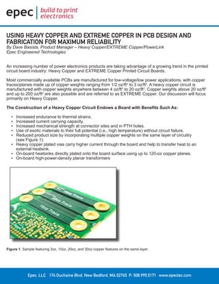
  • 1. Epec, LLC 174 Duchaine Blvd. New Bedford, MA 02745 P: 508.995.5171 www.epectec.com USING HEAVY COPPER AND EXTREME COPPER IN PCB DESIGN AND FABRICATION FOR MAXIMUM RELIABILITY By Dave Basista, Product Manager – Heavy Copper/EXTREME Copper/PowerLink Epec Engineered Technologies An increasing number of power electronics products are taking advantage of a growing trend in the printed circuit board industry: Heavy Copper and EXTREME Copper Printed Circuit Boards. Most commercially available PCBs are manufactured for low-voltage/low power applications, with copper traces/planes made up of copper weights ranging from 1/2 oz/ft2 to 3 oz/ft2 . A heavy copper circuit is manufactured with copper weights anywhere between 4 oz/ft2 to 20 oz/ft2 . Copper weights above 20 oz/ft2 and up to 200 oz/ft2 are also possible and are referred to as EXTREME Copper. Our discussion will focus primarily on Heavy Copper. The Construction of a Heavy Copper Circuit Endows a Board with Benefits Such As: • Increased endurance to thermal strains. • Increased current carrying capacity. • Increased mechanical strength at connector sites and in PTH holes. • Use of exotic materials to their full potential (i.e., high temperature) without circuit failure. • Reduced product size by incorporating multiple copper weights on the same layer of circuitry (see Figure 1). • Heavy copper plated vias carry higher current through the board and help to transfer heat to an external heatsink. • On-board heatsinks directly plated onto the board surface using up to 120-oz copper planes. • On-board high-power-density planar transformers Figure 1. Sample featuring 2oz, 10oz, 20oz, and 30oz copper features on the same layer.
  • 2. Epec, LLC 174 Duchaine Blvd. New Bedford, MA 02745 P: 508.995.5171 www.epectec.com Heavy Copper Circuit Construction Standard printed circuit boards, whether double-sided or multilayer, are manufactured using a combination of copper etching and plating processes. Circuit layers start as thin sheets of copper foil (generally 0.5 oz/ ft2 to 2 oz/ft2 ) that are etched to remove unwanted copper, and plated to add copper thickness to planes, traces, pads and plated-through-holes. All of the circuit layers are laminated into a complete package using an epoxy-based substrate, such as FR4 or polyimide. Boards incorporating heavy copper circuits are produced in exactly the same way, albeit with specialized etching and plating techniques, such as high-speed/step plating and differential etching. Historically, heavy copper features were formed entirely by etching thick copper clad laminated board material, causing uneven trace sidewalls and unacceptable undercutting. Advances in plating technology have allowed heavy copper features to be formed with a combination of plating and etching, resulting in straight sidewalls and negligible undercut. Plating of a heavy copper circuit enables the board fabricator to increase the amount of copper thickness in plated holes and via sidewalls. It’s now possible to mix heavy copper with standard features on a single board, also known as PowerLink. Advantages include reduced layer count, low impedance power distribution, smaller footprints and potential cost savings. Normally, high-current/high-power circuits and their control circuits were produced separately on separate boards. Heavy copper plating makes it possible to integrate high-current circuits and control circuits to realize a highly dense yet simple board structure. The heavy copper features can be seamlessly connected to standard circuits. Heavy copper and standard features can be placed with minimal restriction provided the designer and fabricator discuss manufacturing tolerances and abilities prior to final design (Figure 2). Figure 2. 2oz features connect control circuits while 20oz features carry high current loads.
  • 3. Epec, LLC 174 Duchaine Blvd. New Bedford, MA 02745 P: 508.995.5171 www.epectec.com Current Carrying Capacity and Temperature Rise The amount of current a copper circuit can safely carry depends on how much heat rise a project can withstand, since heat rise and current flow are related. When current flows along a trace, there is an I2R (power loss) that results in localized heating. The trace cools by conduction (into neighboring materials) and convection (into the environment). Therefore, to find the maximum current a trace can safely carry, we must find a way to estimate the heat rise associated with the applied current. An ideal situation would be to reach a stable operating temperature where the rate of heating equals the rate of cooling. An IPC formula can be used to model this event. Track Width (inch) Cu Weight (Oz/Ft2) Thickness (Inch) 0.0625 0.1250 0.2500 0.5000 1.0000 2.0000 4.0000 8.0000 16.0000 1 0.0014 4.6 7.6 12.5 20.7 34.2 56.6 93.6 154.7 255.6 2 0.0028 7.6 12.5 20.7 34.2 56.6 93.6 154.7 255.6 422.5 4 0.0056 12.5 20.7 34.2 56.6 93.6 154.7 255.6 422.5 698.4 6 0.0084 16.8 27.8 46.0 76.0 125.5 207.5 343.0 566.9 937.1 8 0.0112 20.7 34.2 56.6 93.6 154.7 255.6 422.5 698.4 1154.4 10 0.0140 24.4 40.3 66.5 110.0 181.8 300.5 496.7 821.1 1357.1 12 0.0168 27.8 46.0 76.0 125.5 207.5 343.0 566.9 937.1 1548.9 14 0.0196 31.1 51.4 84.9 140.4 232.0 383.6 634.0 1047.9 1732.1 16 0.0224 34.2 56.6 93.6 154.7 255.6 422.5 698.4 1154.4 1908.1 18 0.0252 37.3 61.7 101.9 168.4 278.4 460.2 760.7 1257.3 2078.2 20 0.0280 40.3 66.5 110.0 181.8 300.5 496.7 821.1 1357.1 2243.2 24 0.0336 46.0 76.0 125.5 207.5 343.0 343.0 937.1 1548.9 2560.2 28 0.0392 51.4 84.9 140.4 232.0 383.6 634.0 1047.9 1732.1 2863.0 32 0.0448 56.6 93.6 154.7 255.6 422.5 698.4 1154.4 1908.1 3154.0 36 0.0504 61.7 101.9 168.4 278.4 460.2 760.7 1257.3 2078.2 3435.1 40 0.0560 66.5 110.0 181.8 300.5 496.7 821.1 1357.1 2243.2 3707.8 45 0.0630 72.5 119.8 198.0 327.3 541.0 894.3 1478.1 2443.2 4038.3 50 0.0700 78.2 129.3 213.7 353.3 584.0 965.2 1595.5 2637.1 4358.9 55 0.0770 83.8 138.6 229.0 378.6 625.7 1034.3 1709.6 2825.8 4670.8 60 0.0840 147.6 244.0 403.2 666.5 1101.7 1820.9 3009.8 4974.9 70 0.0980 165.0 272.8 450.9 745.3 1231.9 2036.2 3365.7 5563.1 80 0.1120 181.8 300.5 496.7 821.1 1357.1 2243.2 3707.8 6128.6 90 0.1260 198.0 327.3 541.0 894.3 1478.1 2443.2 4038.3 6675.0 100 0.1400 213.7 353.3 584.0 965.2 1595.5 2637.1 4358.9 7204.8 120 0.1680 403.2 666.5 1101.7 1820.9 3009.8 4974.9 8223.0 140 0.1960 450.9 745.3 1231.9 2036.2 3365.7 5563.1 9195.3 160 0.2240 496.7 821.1 1357.1 2243.2 3707.8 6128.6 10130.0 180 0.2520 541.0 894.3 1478.1 2443.2 4038.3 6675.0 11033.1 200 0.2800 584.0 965.2 1595.5 2637.1 4358.9 7204.8 11908.9 Figure 3. Approximate current for given track dimensions (20°C temp rise). IPC-2221A, calculation for current capacity of an external track [1]: I = .048 * DT(.44) * (W * Th)(.725)
  • 4. Epec, LLC 174 Duchaine Blvd. New Bedford, MA 02745 P: 508.995.5171 www.epectec.com Where I is current (amps), DT is temperature rise (°C), W is width of the trace (mil) and Th is thickness of the trace (mil). Internal traces should be derated by 50% (estimate) for the same degree of heating. Using the IPC formula, we generated Figure 3 (see table at end of text), showing the current carrying capacity of several traces of differing cross-sectional areas with a 30°C temperature rise. What constitutes an acceptable amount of heat rise will differ from project to project. Most circuit board dielectric materials can withstand temperatures of 100°C above ambient, although this amount of temperature change would be unacceptable in most situations. Circuit Board Strength and Survivability Circuit board manufacturers and designers can choose from a variety of dielectric materials, from standard FR4 (operating temp. 130°C) to high-temperature polyimide (operating temp. 250°C). A high-temperature or extreme environment situation may call for an exotic material, but if the circuit traces and plated vias are standard 1 oz/ft2, will they survive the extreme conditions? The circuit board industry has developed a test method for determining the thermal integrity of a finished circuit product. Thermal strains come from various board fabrication, assembly and repair processes, where the differences between the coefficient of thermal expansion (CTE) of Cu and the PWB laminate provide the driving force for crack nucleation and growth to failure of the circuit. Thermal cycle testing (TCT) checks for an increase in resistance of a circuit as it undergoes air-to-air thermal cycling from 25°C to 260°C. An increase in resistance indicates a breakdown in electrical integrity via cracks in the copper circuit. A standard coupon design for this test utilizes a chain of 32 plated through holes, which has long been considered to be the weakest point in a circuit when subjected to thermal stress. The TCT results clearly show that the failure rate, no matter what the board material, can become unacceptable. Thermal cycle studies done on standard FR4 boards with 0.8-mil to 1.2-mil copper plating have shown that 32% of circuits fail after eight cycles (a 20% increase in resistance is considered a failure). Boards with exotic materials show significant improvements to this failure rate (3% after eight cycles for Cyanate Ester), but are prohibitively expensive (five to 10 times material cost) and difficult to process. An average surface-mount technology assembly sees a minimum of four thermal cycles before shipment, and could see an additional two thermal cycles for each component repair. Using heavy copper circuits would reduce or eliminate these failures altogether. Plating of 2 oz/ft2 of copper to a hole wall reduces the failure rate to almost zero (TCT results show a 0.57% failure rate after eight cycles for standard FR4 with a minimum of 2.5-mil copper plating). In effect, the copper circuit becomes impervious to the mechanical stresses placed on it by the thermal cycling. Thermal Management As designers strive to obtain maximum value and performance from their projects, printed circuits are becoming more complex and are driven to higher power densities. Miniaturization, use of power components, extreme environmental conditions and high-current requirements increase the importance of thermal management. The higher losses in the form of heat, that’s often generated in the operation of electronics, has to be dissipated from its source and radiated to the environment; otherwise, the components could overheat and failures may result. However, heavy copper circuits can help by reducing the I2R losses and by conducting heat away from valuable components, reducing failure rates dramatically.
  • 5. Epec, LLC 174 Duchaine Blvd. New Bedford, MA 02745 P: 508.995.5171 www.epectec.com In order to achieve proper heat dissipation from heat sources in and on the surface of a circuit board, heatsinks are employed. The purpose of any heatsink is to dissipate heat away from the source of generation by conduction and emit this heat by convection to the environment. The heat source on one side of the board (or internal heat sources) is connected by copper vias (sometimes called "heat vias") to a large bare copper area on the other side of the board. Generally, classical heatsinks are bonded to this bare copper surface by means of a thermally conductive adhesive or in some cases, are riveted or bolted. Most heatsinks are made of either copper or aluminum. The assembly process required for classical heatsinks consists of three labor-intensive and costly steps. The time and work required to complete this process is significant, and the results are inferior to a mechanically automated process. In contrast, built-in heatsinks are created during the printed circuit board manufacturing process and require no additional assembly. Heavy copper circuit technology makes this possible. This technology allows the addition of thick copper heatsinks virtually anywhere on the outer surfaces of a board. The heatsinks are electroplated on the surface and thus connected to the heat conducting vias without any interfaces that impede thermal conductivity. Another benefit is the added copper plating in the heat vias, which reduces the thermal resistance of the board design, realizing that they can expect the same degree of accuracy and repeatability inherent in PCB manufacturing. Because planar windings are actually flat conductive traces formed on copper clad laminate, they improve the overall current density compared to cylindrical wire conductors. This benefit is due to minimization of skin effect and higher current-carrying efficiency. On-board planars achieve excellent primary-to-secondary and secondary-to-secondary dielectric isolation because the same dielectric material is used between all layers, ensuring complete encapsulation of all windings. In addition, primary windings can be spilt so that the secondary windings are sandwiched between the primaries, achieving low leakage inductance. Standard PCB lamination techniques, using a choice of a variety of epoxy resins, can safely sandwich up to 50 layers of copper windings as thick as 10 oz/ft2 . During the manufacture of heavy copper circuits, we are usually dealing with significant plating thicknesses; therefore, allowances must be made in defining trace separations and pad sizes. For this reason, designers are advised to have the board fabricator on board early in the design process. Epec Engineered Technologies has developed a set of design guidelines for heavy copper circuits that give designers a basic overview of what is required. Military Applications Traditionally when PCB's are used in military applications the designer creates the high current circuits by adding duplicate layers of 3 or 4 oz copper in parallel and crossing their fingers that the layers share the current evenly between them. In practice, the sharing is less than ideal so some layers tend to carry a higher percentage of the load and generate higher losses. Overall, the board normally runs hotter than estimated during the design. Utilizing Heavy or EXTREME Copper in creating the high current circuits combined with thicker copper plating in the vias and plated through holes will eliminate the need to add duplicate layers in parallel, thereby eliminating any concern of load sharing among multiple layers. Temperature rise due to losses in the boards can be calculated with greater certainty. The thick copper plating in the holes dramatically reduces failures associated with thermal stress. The result is a cooler running and more reliable PCB.
  • 6. Epec, LLC 174 Duchaine Blvd. New Bedford, MA 02745 P: 508.995.5171 www.epectec.com Heavy Copper, EXTREME Copper or PowerLink Have Been Used in the Following Military Applications: • Weapons Control Systems • Power Supplies for Radar Systems • Primary and Secondary Windings of High Power Planar Transformers • Power Distribution Panels • Battery Charger and Monitoring Systems Power electronics products using heavy copper circuitry have been in use for many years in the military and aerospace industry and are gaining momentum as a technology of choice in industrial applications. It's believed that market requirements will extend the application of this type of product in the near future. References: [1] IPC -2221A