Common Source Characteristics - JFET
•
0 gefällt mir•825 views

Lab Manual at www.docircuits.com - common source characteristics of JFET

Empfohlen
Weitere ähnliche Inhalte
Was ist angesagt?
Was ist angesagt? (20)
Ähnlich wie Common Source Characteristics - JFET
Ähnlich wie Common Source Characteristics - JFET (20)
Mehr von DoCircuits
Mehr von DoCircuits (19)
Kürzlich hochgeladen
Kürzlich hochgeladen (20)
Common Source Characteristics - JFET
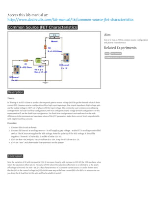
- 1. Access this lab-manual at: http://www.docircuits.com/lab-manual/16/common-source-jfet-characteristics Common Source JFET Characteristics Aim Aim is to bias an FET in common source configuration and plot its characteristics Related Experiments JFET JFET BASICS COMMON SOURCE CHARACTERISTICS Description Theory: DC biasing of an FET is done to produce the required gate-to-source voltage (VGS) to get the desired value of drain current (ID). Common-source configuration offers high input impedance, low output impedance, high voltage gain and the output voltage is 180 ? out-of-phase with the input voltage. The commonly used common-source biasing configurations include fixed-bias configuration, self-bias configuration and voltage-divider configuration. In this experiment we’ll use the fixed-bias configuration. The fixed-bias configuration is not used much as the wide differences in the minimum and maximum values of the JFET parameters make drain current levels unpredictable with simple fixed-bias circuits. Procedure: 1. Connect the circuit as shown. 2. Connect DCSource1 as a voltage source – it will supply a gate voltage – as the FET is a voltage-controlled device. The DCSource0 supplies the VDS voltage. Note the polarity of the VGS voltage. It should be negative. Choose R1 of value 952 Ω and R0 of value 2.05 kΩ. 3. Click on Run > DCAnalysis. Vary VDS from 0 to 10V. Vary the VGS from 0 to 2V. 4. Click on “Run” and observe the characteristics on the plotter Conclusion Note the variation of ID with increase in VDS. ID increases linearly with increase in VDS till the VDS reaches a value where the saturation effect sets in. The value of VDS where the saturation effect sets in is referred to as the pinchoff voltage (at VGS=0). For VDS > VP, JFET has characteristics of a constant current source. It can be further seen that the VGS is the control voltage for JFETs in the same way as the base current (IB) is for BJTs. As an exercise can you draw the dc load line for this plot and find a suitable Q-point?