Materials science, innovation and industry.
•
1 like•1,342 views

Palestra plenária do XI Encontro da SBPMat (Florianópolis, setembro de 2012). Palestrante: Jean Charles Guibert - Minatec (França).

Recommended
Recommended
More Related Content
What's hot
What's hot (20)
Viewers also liked
Viewers also liked (20)
Similar to Materials science, innovation and industry.
Similar to Materials science, innovation and industry. (20)
More from Sociedade Brasileira de Pesquisa em Materiais
More from Sociedade Brasileira de Pesquisa em Materiais (20)
Recently uploaded
Recently uploaded (20)
Materials science, innovation and industry.
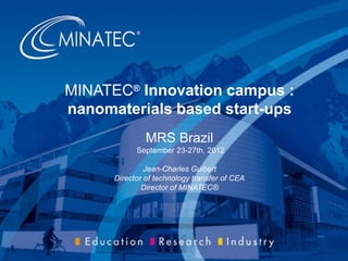
- 1. MINATEC® Innovation campus : nanomaterials based start-ups MRS Brazil September 23-27th, 2012 Jean-Charles Guibert Director of technology transfer of CEA Director of MINATEC® Direction de la valorisation – J.-Ch. GUIBERT 1
- 2. Direction de la valorisation 2
- 3. Evolution of research models Multiple and diverse models are existing : Basics Labs within big firms (IBM, Toshiba, Air liquide, Big pharma,..) Clusters/Industry consortia (Tokai région, Tsukuba,..) RTOs (AIST, CEA (Leti), DoE, FhG, A*STAR, VTT, ITRI, IMEC,..) Networks (EC Nano2life, ..) Academic organization (Indian CoE, CNRS, Max Planck, Academia Sinica, NIMS,..) Universities (various size/goal/models….US land grant univ vs private univ vs french vs Japan or Indian ones) Direction de la valorisation 3
- 4. Evolution of research models : Trends Attractivity for top level PhD / post-docs / researchers Pluri-disciplinarity Increased coordination between the different steps of research Efficient transfer procedures Long-term investment capacity Taking into account society needs Standard and affordable governance bodies Direction de la valorisation 4
- 5. The innovation campus: a new model for the future Research Organization Cluster Techno Park Country size x 1000km size 100km size 10km Industry R&D + fab Research Inst., Industry, University COLLABORATION Multiple locations Research Institutions SHARED SERVICES NATIONAL INNOVATION CAMPUS size 1km Education University Colleges Research Upstream & Technological Research Direction de la valorisation Industry ONE-STOP SHOP 1 OPERATOR R&D labs, start-ups 5
- 6. Grenoble Ecosystem Cluster & Innovation campus Direction de la valorisation – J.-Ch. GUIBERT 6
- 7. Where is Grenoble ? European Union 455,000,000 people France 60,200,000 people Grenoble Rhône-Alpes Region (+urban area) 650,000 people Direction de la valorisation (#2 in France) 5,893,000 people 7
- 8. Grenoble : a historical high tech industrial area Genève Lyon METIS PHOTOWATT Bourgoin-Jallieu Chambéry INES ST MICROELECTRONICS TRONIC’S Voiron SOITEC RADIALL Crolles Grenoble S&T Park THALES XEROX Innovallée BIOMERIEUX CAP GEMINI FT R&D SCHNEIDER ST MICROELECTRONICS Claix SUN BD MGE UPS Gardanne Direction de la valorisation – J.-Ch. GUIBERT CMP Georges Charpak Nice 8
- 9. MINATEC campus – from labs to shared platforms ® TTO Direction de la valorisation 9
- 10. Dedicated platforms per activity 1 2 Advanced CMOS 200 Design Nanotec 300 Showroom Cable-car MEMS 200 Nano-Caractérisation NanoBioTech Energie Leti 2011 | 10 © CEA 2011. Tous droits réservés
- 11. MINATEC campus: key figures 1.5 B€ invested in 10 years for research facilities Research 2,400 people Education 1,400 people (560 PhDs & post-docs) Attractivity Inter-disciplinarity Skills for the future Creativity Technology Transfer • > 3000 research staff • > 1000 students • Annual Budget: 350 M€ Industry & contracts: >60% • 10 000m² cleanrooms Direction de la valorisation Industry 600 people Technology transfer & industrial partnerships Jobs creation • 20 joint laboratories • ~ 300 new patents / year • 1600 scientific publications / year • 400+ graduates MS/PhD 11
- 12. MINATEC platform Education – Research – Industry From Nanolab to Minatec Enterprise Direction de la valorisation – J.-Ch. GUIBERT 12
- 13. Education – Phelma Engineering School PHysics ELectronics MAterials • Part of Grenoble INP group • > 1200 students, 200 professors • First European Master in micronanotechnologies (time share with EPFLausanne & Politecnico de Torino) • • Direction de la valorisation Initial training Professional training 13
- 14. Education – CIME Nanotech • • 2500m² platform dedicated for training activities (700m² cleanrooms) • Materials & Components) 10M€ initial investment • Training for local and foreign companies (Saudi Electronics Annual budget: 2.5M€ (1M€ running costs) • 1300 students studied on the platform in 2008 • Dedicated actions for high school Direction de la valorisation 14
- 15. Research – Upstream research Platform • Dedicated facilities for upstream research (University, CEA, CNRS,..) Direction de la valorisation 15
- 16. Research – Nanocharacterization platform A unique in-line & off-line platform in Europe • 100 people, 1500m² cleanrooms, 3M€/yr investments • 40 heavy equipments, 80 in-line equipments (100 à 300mm) • Cooperation with eqt suppliers (Titan from FEI) Assets of the platform • Dedicated research team on caracterisation • Close to large research infrastructures (Synchrotron, neutrons,..) • Collaboration with both upstream and technological research teams Photos: CEA/DPTS Direction de la valorisation 16
- 17. Technological Research - Nanotec 300 & MEMS 200 platforms More moore & 3D 300 platform / More than Moore 200 platform • Operated by LETI - Equipment sharing with start-ups • 24/7 operation - Proof of concept, prototyping, pre-production • Industrial partnerships - From process step to packaging Photos: P. Guillaume Direction de la valorisation 17
- 18. Industrial R&D labs on-site • A dedicated building for industrial partners • Offices, laboratories and cleanrooms to rent In permanent contact with our research teams Access to common MINATEC facilities Direction de la valorisation 18
- 19. Technology Transfer – « Maison MINATEC » Research trends: Observatory for Micro-Nanotechnologies ( OMNT ) Strategic Marketing Competitive Intelligence Networking and projects: Minalogic Cluster office, SEMI Patents : engineers, lawyers Technology transfers and contracts Investments – Start ups • A unique gathering in Europe: 150 people involved in technology transfer activities in micro and nanotechnologies Photos: P. Conche Direction de la valorisation 19
- 20. International official delegations 2 official delegations week to discover our campus... # 30k visitors in 2010 Direction de la valorisation 20 Strong increase in foreign PhD, scientists
- 21. Nanomaterials based start-ups Direction de la valorisation – J.-Ch. GUIBERT 21
- 22. STMicroelectronics : the world’s fifth largest semiconductor company ST aims to be the undisputed leader in multimedia convergence and power applications leveraging its vast array of technologies, design expertise and combination of intellectual property portfolio, strategic partnerships and manufacturing strength. 2008 sales : US$ 9.84 billion R&D : US$ 2.152 billion (mainly in the areas of product design, technology and development) Approx 50,000 employees in the Group 13 main production sites 16 advances R&D centers Approximate percentage of ST’s sales in 2008 Communication Industrial 36% 17% Automotive 15% Computer Consumer 16% 17% Share R&D business model => partnership with CEA LETI including for example : - Consortium NANO 2012 : development of new technologies fort the creation and production of the next generation of embedded circuits - Crolles II program : Partnership with Freescale / NXP and CEA LETI : creation of a 300mm pilot line and an R&D Technology Center that developed 90nm, 65nm and 45nm CMOS semiconductor technologies. R&D alliance with IBM to develop core 32nm and 22nm CMOS tech and derivative technologies. Work with CEA Leti in Crolles and Grenoble. - Centre Commun de Microelectronique de Crolles : laboratory in partnership with CEA /LETI
- 23. SOITEC N°1 wwide for SOI André-Jacques Auberton-Hervé et Jean-Michel Lamure, anciens ingénieurs du CEA-Leti, créent SOITEC en 1992 French international industrial leader in the generation and production of semiconductor materials for extreme performance, in the heart of electronics and energy challenges. ▪ Staff 2012 : > 1600 personnes ▪ Revenue 2010/2011 : 500 M€ ▪ Common lab CEA Leti-Soitec from 1991. Des partenaires mondiaux III-V Epitaxy Stacking™ Smart Cut™ Smart Stacking™ Photovoltaïque à concentration
- 24. SOFRADIR - ULIS French company which manufactures infrared detectors used in among other military equipment (infrared detection, night vision ...) and aerospace. 1st in this field in Europe. Philippe Bensussan Jean-Luc Tissot • Effectif 2010 : 370 personnes • CA 2010 : ≈ 80 M€ • Laboratoire commun avec le Léti Image visible "naturelle" • Effectif 2010 : 120 personnes • CA 2010 : ≈ 40 M€ • Laboratoire commun avec le Léti Image infra-rouge
- 25. CROCUS O. Redon JP. Nozieres B. Dieny Fondateurs CEA Crocus Technology is a leader in Magnetic Random Access Memory ("MRAM") products and technologies for the semiconductor and electronic systems industries. Crocus MRAM is ideal for a wide range of applications requiring high reliability, high endurance, high read/write speed, or cost effective non-volatile memory. Crocus’ MRAM technology will be available as both standalone devices and embedded memory solutions. • Effectifs 2010 : ≈ 30 personnes - 15 à Grenoble (matériaux, caractérisation, R&D amont) - 15 en Californie (design, commercial et fabrication) • CA 2010 : NS Crocus Technology Strikes $300 Million Financing Deal with RUSNANO to Build Advanced MRAM Manufacturing Facility in Russia
- 26. ETHERA ETHERA develops and markets kits that simplify the diagnosis and monitoring of chemical pollution of the air inside buildings La qualité de l’air intérieur : un enjeu de société majeur Des sources de pollution chimique omniprésentes Yves BIGAY Sylvain COLOMB Produits ménagers, Peintures, Moquettes, Vernis, Meubles, etc… Bâtiments de plus en plus hermétiques Une pollution de l’air intérieur jusqu’à 10x supérieure à celle de l’air extérieur • Effectif 2010 : 8 personnes • CA 2010 : NC Pour des économies d’énergie Les capteurs nanoporeux : une technologie unique CEA-CNRS Des matériaux dont la couleur varie linéairement en fonction de la quantité de polluant piégée Ex : Bureau de 65 m3, Formaldéhyde: 50 ppb, ETHERA s’appuie sur des brevets du CEA et du CNRS Thu-Hoa TRAN-THI
- 27. CYTOO Distinctive life sciences systems& tools company that currently offers a disruptive solution that brings robustness, sensitivity and powerful quantification to cell-based assays and High Content Screening (HCS). François Chatelain Alexandra Fuchs Michel Bornens • Effectif 2010 : 22 personnes • CA 2010 : NC Throughout the CYTOO micropattern array, cells adopt the same architecture. Immediate benefits: Straightforward analysis, reliable results and faster discovery Cellules dans une boîte de culture standard Cellules cultivées sur les produits CYTOO Application assays: Cell biology and high throughput screening
- 28. ISORG ISORG is pionniering Printed Organic Electronics for photodetectors and large surface image sensors. Its technology is a brandly new one patented by CEA. Jean-Yves Gomez Emmanuel Guérineau Laurent Jamet This technology moves plastic and glass in an intelligent surface able to interact with the connected world. • Staff 2012 : 20 persons • CA 2011 : NA ISORG vision goals to develop and produce in volume printed organic components for multiple market segments. International leadership is planned.
- 29. ALCHIMER ALCHIMER is dedicated to providing innovative, wet-based deposition technology that delivers higher-quality surfaces with lower cost of ownership than legacy vaporphase technologies (PVD, CVD and ALD). Alchimer’s deposition technology is engineered at the molecular level for high performance at much lower cost – typically 60 percent less than PVD. The Electrografting (eG™) and Chemicalgrafting (cG™) processes produce outstanding conformal coatings even over complex structures, using economical industry-standard process equipment. • Staff 2011 : 10 • Turnover 2011 : 300 K€
- 30. FLUOPTICS Developping new solutions for guided surgery Focused on cancer surgery improvement, Fluoptics technology will give surgeons a radically new efficiency in tumor resection. Fluoptics has developed an imaging system that will drastically improve cancer surgery, giving new hope to thousands of cancer patients around the world. The technology is based on an intraoperative fluorescence detector and fluorescent probes which specifically target tumors. Staff 2011 : 11 employees Turnover 2011 : 560 K€
- 31. NANOMAKERS NANOMAKERS designs, produces and sells SiC nanopowders of high quality that increase decisively the mechanical, thermal and chemical materials of all types of industrial. • Staff 2011 : 5 employees (France) 2 employees (Japan) • Turnover 2011 : 90 K€ Highlight 2011 Nanopowders of silicon carbide are compatible with a wide range of materials. It can be incorporated into polymers, metals, ceramics. Nanopowders are the material of choice to enhance many existing materials or develop new ones. → Fundraising : 3,3 M€ → Design, installation of the first block on the production site CONTINENTAL in Rambouillet. The commissioning was completed January 9, 2012 with rates of production and quality above expectations. → Majority stake in Japan Nanomakers and early commercial deployment in Europe and North America.
- 32. APIX TECHNOLOGY Analytical Pixels Technology APIX is the first startup to be spun out of the Alliance for Nanosystems VLSI, which was launched by Leti and the California Institute of Technology in 2007. • Staff 2011 : 4 • Turnover 2011 : - APIX designs, manufactures and markets analysis tools based on nanoelectromechanical systems (NEMS) and an innovative way to implement miniaturized gas chromatography. These tiny systems will significantly reduce the costs of current gas analysis systems used for industrial processing by the petrochemical and natural gas distribution industries and for analysis of ambient air quality. Future applications are expected to include health screening through the analysis of biomarkers in a patient’s breath..
- 33. Conclusion • Materials were, are and will be at the core of multiple applications. • Start-up is the way to move invention into innovations for the market. • CEA created more than 70 material based companies • MINATEC innovation campus is a place designed and organised for innovative start-ups efficient growth. • Investment in these start-ups goals and assures multiple long-term partners for long term R&D contracts.
- 34. MINATEC Nanolab network Direction de la valorisation – J.-Ch. GUIBERT 34
- 36. Nanotechnologies are key for the development of future industries Nanotechnology potential world market size by 2015 is around 1 trillion US dollars (NSF) Multiple fields of application Multiple goals and interest for the country development - systems textile industry automotive electronics Create start-ups - Develop a culture of Innovation - How ? Generate Intellectual Properties - (& rare ones) Develop and assist Research - materials Support an existing industry - Country strategic goals Youth training - energy Strategic independence … Time ? healthcare Large and difficult project to achieve without long field experience Time delays without an efficient master planning MINATEC® Nanolab presentation _ 2012 36
- 37. A complete full-packaged project-oriented approach to develop a research facility in nanotechnologies - Country strategic goals ENABLER = MINATEC® Nanolab A project-oriented approach Engineered by an experienced public-private consortium 24 months Strategic independence - Youth training - Support an existing industry - Develop and assist Research - Generate Intellectual Properties - Create start-ups - Develop a culture of Innovation - … + Become a member of the international network MINATEC® Nanolab MINATEC® Nanolab presentation _ 2012 37
- 38. MINATEC® Nanolab, a 24 months 3 phases packaged procedure with well-defined deliverables 1 DEFINITION Analysis & studies 6 months - Strategy and marketing positioning, definition of fields of application - Writing of a basic design, (ie. Definition of the plateform, the equipments, training plans,etc.) and a first previsional budget - Writing of a detailed design, with implementation plans Specification listing with provisional budget 2 SETTING UP Except civil ingineering Until operational 18 months - Detailed answer and quotations: - equipment, facilities, … - technical & maintenance and process engineers training Contract 3 RESEARCH ORIENTED PROJECT MODE Long term - Integration in MINATEC® Nanolab International Network - students and researchers exchanges - common purchase center - developments i.e training in tech transfer - Implementation: - purchasing and installation - training - implementation - Validation phase on demonstrators Acceptance on specifications MINATEC® Nanolab presentation _ 2012 MINATEC® Nanolab International Network 38
- 39. MINATEC TOMORROW Direction de la valorisation – J.-Ch. GUIBERT 39
- 40. Grenoble’s success stories GIANT A unique campus of 250 ha In the heart of the city of Grenoble With state-of-the-art equipments for science and technology Major research and education institutions Attracting researchers from all around the world And a strong involvement of local and regional authorities GIANT offers a great synergy of technological means and human resources Direction de la valorisation 40
- 41. GIANT’s vision Six centers of excellence Micro-nanotechnology MINATEC Management Large European instruments Energy GreEn Health and biotech Nanobio Fundamental research Direction de la valorisation 41
- 42. GIANT’s vision, an ambitious urban transformation Creating a dynamic and attractive campus Direction de la valorisation 42
- 43. GIANT Key figures Annual Budget: 1000M€ (Investments : 150 M€) 10 000 researchers 10 000 students 10 000 inhabitants 7 000 industrial jobs Rank 4th for patents in France 5 000 scientific publications / year 500 new patents / year Direction de la valorisation 43
- 44. GIANT: Coupled to a huge urban development project Direction de la valorisation 44
- 45. MERCI T HANK Y OU Direction de la valorisation – J.-Ch. GUIBERT 45