1. CONCLUSIONS AND FUTURE PLANS
CHARACTERIZATION BY AFM
ELECTROSTATIC FORCE MICROSCOPY
ATOMIC FORCE MICROSCOPY
Topography = (A+B)-(C+D)
INTRODUCTION
ACKNOWLEDGMENT
Topography Phase
SYNTHESIS AND AFM CHARACTERIZATION OF DESIGNED NANOSTRUCTURES OF CERIUM OXIDE
Azzy L. Francis, Steve M. Deese, and Jayne C. Garno*
Department of Chemistry, Louisiana State University, Baton Rouge, LA 70803
The authors gratefully acknowledge support from
the National Science Foundation Career/PECASE
award (CHE-0847291); the Camille Dreyfus
Teacher-Scholar award; the Petroleum Research
Fund of the American Chemical Society; and IMSD
Research Scholars Program.
Test platforms of cerium oxide nanoparticles were examined to determine
electrical properties such as surface potential using Electrostatic Force
Microscopy (EFM). With high special resolution, the EFM is commonly used to
map electrical properties on a sample surface by measuring the electrostatic force
between the sample surface and a biased atomic force microscope (AFM)
cantilever. EFM yields information of electrical properties of a sample while
simultaneously providing topography details. Phase and amplitude images are
acquired simultaneously while topography frames sensitively disclose fine details
of the surface morphology. Studies with EFM enabled measurements of potential
energy differences with nanoscale resolution thereby enabling tracking differences
in oxidation state of the material. Our goals were to apply scanning probe
characterizations of nanoparticle test platforms to investigate electrical properties
at the level of individual cerium oxide nanoparticles.
2Li, G; Mao, B; Lan, F; Liu, L. Review of Scientific Instruments, 2012, 83, 113701(1) – 113701(8).
In EFM, a conductive AFM tip (coated with Pt) is biased with a dc voltage (Vdc) and an
ac voltage (Vac) at a frequency (ωe). The dc and ac electrical drive on the tip causes
an electrostatic force between the tip and the sample surface. The electrostatic force
at the electrical driving frequency can be described as
F(ωe) = ∂C/∂z (ϕ + Vdc)Vacsin(ωet) (1)
Where C is the capacitance between tip and sample surface, and ϕ is the contact
potential difference between tip and sample surface. The electrostatic force F(ωe)
causes the cantilever to oscillate at a certain frequency (ωe). The amplitude of the
cantilever oscillation at the frequency can be detected by a lock in amplifier. Using a
feedback control to adjust the dc bias, the electrostatic force F(ωe) can be nullified
thus the cantilever oscillation can be minimized. Therefore, the surface contact
potential difference can be acquired from the dc bias ϕ = -Vdc.
CERIUM OXIDE NANOPATICLE SYNTHESIS
1Chen, P; Chen, I. Journal of the American Ceramic Society, 1993, 76, 1577-1583.
In the Ce-urea method, 0.5 M urea was dissolved in a 0.008 M cerium
nitrate solution. The solution was then heated to 85 ± 1 °C for 1 h to effect
precipitation.
T h e a t o m i c f o r c e
microscope (AFM) was
u s e d t o i m a g e t h e
substrate surfaces.
When imaging in contact
mode AFM, the tip is
attached to the end of a
cantilever and makes soft,
physical contact with the
substrate surface.
As the tip scans the
substrate surface, the
cantilever attached to the
tip bends to accommodate
to the changes in height
on the substrate’s surface.
125 nm
200 nm
140 nm
125 nm 0 nm
150 nm
200 nm 0 nm 0 0
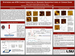
CHARACTERIZATION BY EFM
60 nm 0.23 V
300 nm 300 nm300 nm
Topography Phase Surface Potential
0
0
60 nm
0.06
0.07
0.08
0.09
0.1
0.11
0.12
0.13
0.14
0.15
0.16
0 0.1 0.2 0.3 0.4 0.5
Voltage(V)
Distance (µm)
0.2 V
200 nm
200 nm
200 nm
Electrostatic fields between tip and sample detected by
monitoring the amplitude response of the cantilever at ωe.
The cantilever is
oscillated at a
mechanical resonant
frequency ωmech.
AC bias applied
between the tip and
sample at electrical
resonant frequency
ωe.
Additional
electrostatic forces
caused by the AC
bias influence the
tapping amplitude of
the tip.
0 nm 0 nm
Topography Phase
Surface Potential
1.25 µm 1.25 µm
42 nm
0 nm
Topography Phase
• Atomic force microscopy is an ideal instrument to characterize
cerium oxide nanoparticles due to its high resolution in three
dimensions.
• The Keysight 5500 AFM/EFM instrument was setup correctly as
proven by the images acquired.
• Electrostatic force microscopy served as an model method mapping
out surface potential differences while simultaneously providing
topography details.
• Future plans include to drop-deposit two types of nanoparticles on a
silicon surface and image with EFM. Rare earth nanoparticles
having difference work functions should be distinguishable using
EFM. Further investigations will be done to determine surface
potential as a function of nanoparticle size.
510
560
610
660
0.0 0.2 0.4 0.6
Height(nm)
Distance (µm)
0.0
O
H2N NH2
Ce(NO3)3 Ÿ 6H2O
Heat
85 °C
The recovered cerium oxide
nanoparticles where drop deposited on
silicon (111) substrates and oven dried
at 150 °C.
Cerium oxide nanoparticles were drop
deposited on silicon. Topography and
phase images were acquired using
tapping-mode AFM for different areas.
The cerium oxide nanoparticle selected for
height measurements measure 50 – 60 nm in
height. The cursor profile shows a width of
~250 nm for this particular nanoparticle.
50