SlideShare ist ein Scribd-Unternehmen logo
1 von 13
Diodes - Simple Applications Why would you want the equivalent of an electronic check-valve?
Diode Current-Voltage relationship The characteristics of all silicon based diodes are effectively the same, showing a sharp exponential increase in current at forward bias and only a few   As at reverse bias. Note that this “knee” is temperature-dependent as observed in lab 1. The non-ideal behavior shows a slower than exponential increase due to a series resistance, like the inductor. At large reverse-bias (not shown) current starts to flow.  We will discuss this region later. 1N4148 characteristics
Diode models A diode is often approximated as a 2-terminal device with ~0.7 v drop as long as 1-100 mA are flowing in the forward direction.  The curves for a typical switching signal diode show why this is OK (note the log scale for current).  When it is either reverse or weakly forward biased it is modeled as an open circuit. Real diodes and the symbol are shown.  The arrow points in the direction of forward current flow.
More Diode Physics Pure semiconducting materials like Silicon have very high resistivity at room temperature.  However it can be made conductive by adding extra electrons.  In n-type material this is done via atoms with one more electron than silicon (phosphorus).  It can also be more conductive if one electron is removed, allowing the resulting “holes” to move about (they are really absences of valence or bonding electrons that hop from one site to the next).  This is done in p-type material by adding elements with one less electron (aluminum).  This is known as doping. An interesting thing happens if p- and n-type material are in contact.  A region that has no holes on the p-side and no electrons on the n-side forms, called the depletion region.  This area is like the original pure semiconductor and does not conduct, making the junction a very poor conductor again.  However if it is biased (meaning a voltage is applied) with the p-type positive relative to the n-type, the depletion region shrinks. This is the origin of the one-way flow.  The next slides describe why this is, using images from the website  http://jas.eng.buffalo.edu/
Diode Current-Voltage relationship (1) When material with lots of electrons (n-type) is brought into contact with material with lots of holes (p-type) the electrons and holes diffuse, resulting in a large current.  However the loss of these carriers leaves a depleted region that is charged (because of the P and Al ions left behind) and reduces the current since the electric field repels the carriers.
Diode Current-Voltage relationship (2) At zero bias electrons (holes) flow left (right) because of diffusion and an equal amount flow right (left) due to the electric field, resulting in no current.  As the depletion region increases with reverse bias (not shown), the diffusion current to the left decreases leaving only a small reverse saturation current due to the field. Notice that for these doping levels the depletion region is 0.15 microns thick.
Diode Current-Voltage relationship (3) At positive bias the depletion region is reduced and many electrons (holes) diffuse left (right) while only a small amount flow right (left) due to the electric field, resulting in a large current (sum of holes and electrons) flowing right. When an electron gets to the p-type material it recombines with a hole.  If it does this in the depleted region the ideality factor N is 2, while it is 1 if recombination occurs outside.  The depletion region is now only  0.05 microns thick.
Types of diodes   Power diodes (or rectifiers)  - designed to handle large currents, typically used on power supplies or for switches.  Typical values (for 1N4002) Max Average current: 1 A Peak current: 30 A Reverse voltage: 100 v Signal diodes  - low powered, often faster switching (smaller depletion region).  Typical values (for 1N4148) Max Average current: 100 mA Peak current: 450 mA Reverse voltage: 75 v Recovery time: 4 ns Zener diodes  - voltage regulation, similar to power diodes but has any important specification: the zener voltage, V z  (more later).  Designed to breakdown at precise voltage (range 1-400 v).
Clamp (or clipper)  What does this circuit do?  As mentioned in the text it “clamps” or “clips” the output voltage.  If the magnitude of the input exceeds V batt +0.7 v, either negative or positive, the diode starts conducting.  This limits the maximum voltage (this is similar to surge protectors). V bat One limitation of this is that by design it will distort a time-varying voltage input, cutting it off at a max and a min value. V in R V out
Stiff Clamp  V in C V out This circuit on the other hand works very well at higher frequencies in limiting the minimum voltage on the output.  Treating the diode like a simple one-way switch we see that the output can never fall below -0.7 v, because then the diode begins conducting. How does the circuit do this?  If the input voltage is less than this minimum, current flows counterclockwise, charging the left capacitor plate negative and the right plate positive.  This capacitor voltage adds to the input, raising it to a minimum of -0.7 v, when current stops flowing.  Note that it is the opposite if the diode is reversed because the currents flow clockwise.
Zener diode - IV characteristics All diodes show a breakdown under reverse bias when the internal electric field gets very high, ripping electrons from atoms.  This avalanche breakdown occurs typically at -50 to -1000 v. If the depleted region that acts like a barrier to current is thin there is another possibility.  The electrons can quantum mechanically tunnel from the n- to the p-side, resulting in a reverse current.  This can be engineered to occur at a precise voltage called the Zener voltage, V Z . V I V Z I II III The graph shows three distinct regions, as labeled.  Region III is where zener diodes normally operate.
Zener diode - voltage regulator (1) How can a zener regulator act to control the output voltage?  In the circuit shown (note that the zener is connected so that it is  reverse biased ) current flows through the zener and it is in region III, so the voltage drop across it is V Z . A zener only works as a regulator because it ensures that enough current is drawn through the series resistor so that the voltage drop results in V out =V Z . If no current flows through the zener (actually less than a few mAs) it no longer regulates because it is in region II. V out Unregulated V in
Zener diode - voltage regulator (2) The voltage across the load is V Z  since there is current through the zener (Region III) R R The voltage on the load is R load /(R+R load )V in  because there is no current through the zener. R load Unregulated V in R load Unregulated V in

Weitere ähnliche Inhalte

Was ist angesagt?

Was ist angesagt? (20)

I v characteristics of zener diode
I v characteristics of zener diodeI v characteristics of zener diode
I v characteristics of zener diode
 
Zenerdiode
ZenerdiodeZenerdiode
Zenerdiode
 
Zener diode
Zener diodeZener diode
Zener diode
 
Led prp
Led prpLed prp
Led prp
 
BEE introduction slides
BEE introduction slidesBEE introduction slides
BEE introduction slides
 
Zener diode 212
Zener diode  212  Zener diode  212
Zener diode 212
 
Zener diode
Zener diode Zener diode
Zener diode
 
02 zenerdiodes ppt_prp
02 zenerdiodes ppt_prp02 zenerdiodes ppt_prp
02 zenerdiodes ppt_prp
 
Zener voltage regulator
Zener voltage regulatorZener voltage regulator
Zener voltage regulator
 
Zener Diodes
Zener DiodesZener Diodes
Zener Diodes
 
Diode
DiodeDiode
Diode
 
Zener diode voltage regulator (ALIV - Bangladesh)
Zener diode voltage regulator (ALIV - Bangladesh)Zener diode voltage regulator (ALIV - Bangladesh)
Zener diode voltage regulator (ALIV - Bangladesh)
 
Zener diode
Zener diodeZener diode
Zener diode
 
Zener diode and its applications
Zener diode and its applicationsZener diode and its applications
Zener diode and its applications
 
Zener diode as voltage regulator
Zener diode as voltage regulatorZener diode as voltage regulator
Zener diode as voltage regulator
 
The p n Junction Diode (Basic Electronics)
The p n Junction Diode (Basic Electronics) The p n Junction Diode (Basic Electronics)
The p n Junction Diode (Basic Electronics)
 
Full sessional pack ii
Full sessional pack iiFull sessional pack ii
Full sessional pack ii
 
Zener diode
Zener diodeZener diode
Zener diode
 
zener diodes
 zener diodes zener diodes
zener diodes
 
Zener diode
Zener diodeZener diode
Zener diode
 

Andere mochten auch

Photochemistry
PhotochemistryPhotochemistry
Photochemistry
vivek
 
Semiconductor Devices Class 12 Part-1
Semiconductor Devices Class 12 Part-1Semiconductor Devices Class 12 Part-1
Semiconductor Devices Class 12 Part-1
Self-employed
 
States Of Matter Power Point
States Of Matter Power PointStates Of Matter Power Point
States Of Matter Power Point
wolffer87
 
Solar panel Technology ppt
Solar panel Technology pptSolar panel Technology ppt
Solar panel Technology ppt
Gourav Kumar
 

Andere mochten auch (20)

Circuit labthermistors (1)
Circuit labthermistors (1)Circuit labthermistors (1)
Circuit labthermistors (1)
 
Poster template 1314
Poster template 1314Poster template 1314
Poster template 1314
 
Led Theory and Working Principles
Led Theory and Working PrinciplesLed Theory and Working Principles
Led Theory and Working Principles
 
LCD Theory and Working Principles
LCD Theory and Working PrinciplesLCD Theory and Working Principles
LCD Theory and Working Principles
 
Zener diode
Zener diodeZener diode
Zener diode
 
Photochemistry
PhotochemistryPhotochemistry
Photochemistry
 
Photochemistry
PhotochemistryPhotochemistry
Photochemistry
 
Zener diode as a voltage Regulator
Zener diode as a voltage RegulatorZener diode as a voltage Regulator
Zener diode as a voltage Regulator
 
Pn junction diode characteristics Lab expriment
Pn junction diode characteristics Lab exprimentPn junction diode characteristics Lab expriment
Pn junction diode characteristics Lab expriment
 
CBSE Class XII physics practical project on Metal detector
CBSE Class XII physics practical project on Metal detectorCBSE Class XII physics practical project on Metal detector
CBSE Class XII physics practical project on Metal detector
 
Pn junction diode
Pn junction diodePn junction diode
Pn junction diode
 
Diode
DiodeDiode
Diode
 
Semiconductor Devices Class 12 Part-1
Semiconductor Devices Class 12 Part-1Semiconductor Devices Class 12 Part-1
Semiconductor Devices Class 12 Part-1
 
Diodes
DiodesDiodes
Diodes
 
Semiconductor physics
Semiconductor physicsSemiconductor physics
Semiconductor physics
 
States Of Matter Power Point
States Of Matter Power PointStates Of Matter Power Point
States Of Matter Power Point
 
Physics semiconductors project
Physics semiconductors projectPhysics semiconductors project
Physics semiconductors project
 
Physics investigatory project on RECTIFIER
Physics investigatory project on RECTIFIERPhysics investigatory project on RECTIFIER
Physics investigatory project on RECTIFIER
 
Solar panel Technology ppt
Solar panel Technology pptSolar panel Technology ppt
Solar panel Technology ppt
 
Solar tree ppt
Solar tree pptSolar tree ppt
Solar tree ppt
 

Ähnlich wie anery-Whats Diode

Tunnel Diode (Esaki Diode )
Tunnel Diode (Esaki Diode )Tunnel Diode (Esaki Diode )
Tunnel Diode (Esaki Diode )
Soudip Sinha Roy
 
Diode data sheet for alarm type project
Diode data sheet for alarm type projectDiode data sheet for alarm type project
Diode data sheet for alarm type project
megha agrawal
 
pn-junctiondiodeJJNINIIJOIOOIMOMOKMOMOIM
pn-junctiondiodeJJNINIIJOIOOIMOMOKMOMOIMpn-junctiondiodeJJNINIIJOIOOIMOMOKMOMOIM
pn-junctiondiodeJJNINIIJOIOOIMOMOKMOMOIM
Saravanan Pazapughal
 
A BASIC INTRODUCTION TO SEMICONDUCTOR DEVICES - THE
A BASIC INTRODUCTION TO SEMICONDUCTOR DEVICES - THEA BASIC INTRODUCTION TO SEMICONDUCTOR DEVICES - THE
A BASIC INTRODUCTION TO SEMICONDUCTOR DEVICES - THE
Winston Bent A.S.S.
 

Ähnlich wie anery-Whats Diode (20)

Basic of Electronics study materials
Basic of Electronics study  materialsBasic of Electronics study  materials
Basic of Electronics study materials
 
8. semiconductors.rr
8. semiconductors.rr8. semiconductors.rr
8. semiconductors.rr
 
Chapter2
Chapter2Chapter2
Chapter2
 
Theory of solids
Theory of solidsTheory of solids
Theory of solids
 
Diodes
DiodesDiodes
Diodes
 
Diode
DiodeDiode
Diode
 
Bsc 1 cbcs e1 unit 2
Bsc 1 cbcs e1 unit 2Bsc 1 cbcs e1 unit 2
Bsc 1 cbcs e1 unit 2
 
Semiconductors
SemiconductorsSemiconductors
Semiconductors
 
Semiconductor diodes
Semiconductor diodesSemiconductor diodes
Semiconductor diodes
 
Cro ppt
Cro pptCro ppt
Cro ppt
 
Tunnel Diode (Esaki Diode )
Tunnel Diode (Esaki Diode )Tunnel Diode (Esaki Diode )
Tunnel Diode (Esaki Diode )
 
the-blocking-diode.pdf
the-blocking-diode.pdfthe-blocking-diode.pdf
the-blocking-diode.pdf
 
Diode data sheet for alarm type project
Diode data sheet for alarm type projectDiode data sheet for alarm type project
Diode data sheet for alarm type project
 
pn-junctiondiodeJJNINIIJOIOOIMOMOKMOMOIM
pn-junctiondiodeJJNINIIJOIOOIMOMOKMOMOIMpn-junctiondiodeJJNINIIJOIOOIMOMOKMOMOIM
pn-junctiondiodeJJNINIIJOIOOIMOMOKMOMOIM
 
V-i characteris (1).pdf
V-i characteris (1).pdfV-i characteris (1).pdf
V-i characteris (1).pdf
 
A BASIC INTRODUCTION TO SEMICONDUCTOR DEVICES - THE
A BASIC INTRODUCTION TO SEMICONDUCTOR DEVICES - THEA BASIC INTRODUCTION TO SEMICONDUCTOR DEVICES - THE
A BASIC INTRODUCTION TO SEMICONDUCTOR DEVICES - THE
 
negative-resistance-zone.pdf
negative-resistance-zone.pdfnegative-resistance-zone.pdf
negative-resistance-zone.pdf
 
Difference between half wave and full wave rectifier
Difference between half wave and full wave rectifierDifference between half wave and full wave rectifier
Difference between half wave and full wave rectifier
 
5-digital_electronics1 (1).pdf
5-digital_electronics1 (1).pdf5-digital_electronics1 (1).pdf
5-digital_electronics1 (1).pdf
 
5-digital_electronics1.pdf
5-digital_electronics1.pdf5-digital_electronics1.pdf
5-digital_electronics1.pdf
 

Kürzlich hochgeladen

Call Girls Electronic City Just Call 👗 7737669865 👗 Top Class Call Girl Servi...
Call Girls Electronic City Just Call 👗 7737669865 👗 Top Class Call Girl Servi...Call Girls Electronic City Just Call 👗 7737669865 👗 Top Class Call Girl Servi...
Call Girls Electronic City Just Call 👗 7737669865 👗 Top Class Call Girl Servi...
amitlee9823
 
FULL ENJOY Call Girls In Mahipalpur Delhi Contact Us 8377877756
FULL ENJOY Call Girls In Mahipalpur Delhi Contact Us 8377877756FULL ENJOY Call Girls In Mahipalpur Delhi Contact Us 8377877756
FULL ENJOY Call Girls In Mahipalpur Delhi Contact Us 8377877756
dollysharma2066
 
Call Girls In Noida 959961⊹3876 Independent Escort Service Noida
Call Girls In Noida 959961⊹3876 Independent Escort Service NoidaCall Girls In Noida 959961⊹3876 Independent Escort Service Noida
Call Girls In Noida 959961⊹3876 Independent Escort Service Noida
dlhescort
 
Call Now ☎️🔝 9332606886🔝 Call Girls ❤ Service In Bhilwara Female Escorts Serv...
Call Now ☎️🔝 9332606886🔝 Call Girls ❤ Service In Bhilwara Female Escorts Serv...Call Now ☎️🔝 9332606886🔝 Call Girls ❤ Service In Bhilwara Female Escorts Serv...
Call Now ☎️🔝 9332606886🔝 Call Girls ❤ Service In Bhilwara Female Escorts Serv...
Anamikakaur10
 
Call Girls Jp Nagar Just Call 👗 7737669865 👗 Top Class Call Girl Service Bang...
Call Girls Jp Nagar Just Call 👗 7737669865 👗 Top Class Call Girl Service Bang...Call Girls Jp Nagar Just Call 👗 7737669865 👗 Top Class Call Girl Service Bang...
Call Girls Jp Nagar Just Call 👗 7737669865 👗 Top Class Call Girl Service Bang...
amitlee9823
 
Call Girls Kengeri Satellite Town Just Call 👗 7737669865 👗 Top Class Call Gir...
Call Girls Kengeri Satellite Town Just Call 👗 7737669865 👗 Top Class Call Gir...Call Girls Kengeri Satellite Town Just Call 👗 7737669865 👗 Top Class Call Gir...
Call Girls Kengeri Satellite Town Just Call 👗 7737669865 👗 Top Class Call Gir...
amitlee9823
 
Nelamangala Call Girls: 🍓 7737669865 🍓 High Profile Model Escorts | Bangalore...
Nelamangala Call Girls: 🍓 7737669865 🍓 High Profile Model Escorts | Bangalore...Nelamangala Call Girls: 🍓 7737669865 🍓 High Profile Model Escorts | Bangalore...
Nelamangala Call Girls: 🍓 7737669865 🍓 High Profile Model Escorts | Bangalore...
amitlee9823
 
Insurers' journeys to build a mastery in the IoT usage
Insurers' journeys to build a mastery in the IoT usageInsurers' journeys to build a mastery in the IoT usage
Insurers' journeys to build a mastery in the IoT usage
Matteo Carbone
 
Chandigarh Escorts Service 📞8868886958📞 Just📲 Call Nihal Chandigarh Call Girl...
Chandigarh Escorts Service 📞8868886958📞 Just📲 Call Nihal Chandigarh Call Girl...Chandigarh Escorts Service 📞8868886958📞 Just📲 Call Nihal Chandigarh Call Girl...
Chandigarh Escorts Service 📞8868886958📞 Just📲 Call Nihal Chandigarh Call Girl...
Sheetaleventcompany
 

Kürzlich hochgeladen (20)

Mondelez State of Snacking and Future Trends 2023
Mondelez State of Snacking and Future Trends 2023Mondelez State of Snacking and Future Trends 2023
Mondelez State of Snacking and Future Trends 2023
 
Falcon Invoice Discounting: The best investment platform in india for investors
Falcon Invoice Discounting: The best investment platform in india for investorsFalcon Invoice Discounting: The best investment platform in india for investors
Falcon Invoice Discounting: The best investment platform in india for investors
 
Call Girls Electronic City Just Call 👗 7737669865 👗 Top Class Call Girl Servi...
Call Girls Electronic City Just Call 👗 7737669865 👗 Top Class Call Girl Servi...Call Girls Electronic City Just Call 👗 7737669865 👗 Top Class Call Girl Servi...
Call Girls Electronic City Just Call 👗 7737669865 👗 Top Class Call Girl Servi...
 
FULL ENJOY Call Girls In Mahipalpur Delhi Contact Us 8377877756
FULL ENJOY Call Girls In Mahipalpur Delhi Contact Us 8377877756FULL ENJOY Call Girls In Mahipalpur Delhi Contact Us 8377877756
FULL ENJOY Call Girls In Mahipalpur Delhi Contact Us 8377877756
 
VVVIP Call Girls In Greater Kailash ➡️ Delhi ➡️ 9999965857 🚀 No Advance 24HRS...
VVVIP Call Girls In Greater Kailash ➡️ Delhi ➡️ 9999965857 🚀 No Advance 24HRS...VVVIP Call Girls In Greater Kailash ➡️ Delhi ➡️ 9999965857 🚀 No Advance 24HRS...
VVVIP Call Girls In Greater Kailash ➡️ Delhi ➡️ 9999965857 🚀 No Advance 24HRS...
 
Eluru Call Girls Service ☎ ️93326-06886 ❤️‍🔥 Enjoy 24/7 Escort Service
Eluru Call Girls Service ☎ ️93326-06886 ❤️‍🔥 Enjoy 24/7 Escort ServiceEluru Call Girls Service ☎ ️93326-06886 ❤️‍🔥 Enjoy 24/7 Escort Service
Eluru Call Girls Service ☎ ️93326-06886 ❤️‍🔥 Enjoy 24/7 Escort Service
 
Enhancing and Restoring Safety & Quality Cultures - Dave Litwiller - May 2024...
Enhancing and Restoring Safety & Quality Cultures - Dave Litwiller - May 2024...Enhancing and Restoring Safety & Quality Cultures - Dave Litwiller - May 2024...
Enhancing and Restoring Safety & Quality Cultures - Dave Litwiller - May 2024...
 
Cracking the Cultural Competence Code.pptx
Cracking the Cultural Competence Code.pptxCracking the Cultural Competence Code.pptx
Cracking the Cultural Competence Code.pptx
 
Call Girls In Noida 959961⊹3876 Independent Escort Service Noida
Call Girls In Noida 959961⊹3876 Independent Escort Service NoidaCall Girls In Noida 959961⊹3876 Independent Escort Service Noida
Call Girls In Noida 959961⊹3876 Independent Escort Service Noida
 
Call Now ☎️🔝 9332606886🔝 Call Girls ❤ Service In Bhilwara Female Escorts Serv...
Call Now ☎️🔝 9332606886🔝 Call Girls ❤ Service In Bhilwara Female Escorts Serv...Call Now ☎️🔝 9332606886🔝 Call Girls ❤ Service In Bhilwara Female Escorts Serv...
Call Now ☎️🔝 9332606886🔝 Call Girls ❤ Service In Bhilwara Female Escorts Serv...
 
Call Girls Jp Nagar Just Call 👗 7737669865 👗 Top Class Call Girl Service Bang...
Call Girls Jp Nagar Just Call 👗 7737669865 👗 Top Class Call Girl Service Bang...Call Girls Jp Nagar Just Call 👗 7737669865 👗 Top Class Call Girl Service Bang...
Call Girls Jp Nagar Just Call 👗 7737669865 👗 Top Class Call Girl Service Bang...
 
Call Girls Kengeri Satellite Town Just Call 👗 7737669865 👗 Top Class Call Gir...
Call Girls Kengeri Satellite Town Just Call 👗 7737669865 👗 Top Class Call Gir...Call Girls Kengeri Satellite Town Just Call 👗 7737669865 👗 Top Class Call Gir...
Call Girls Kengeri Satellite Town Just Call 👗 7737669865 👗 Top Class Call Gir...
 
Nelamangala Call Girls: 🍓 7737669865 🍓 High Profile Model Escorts | Bangalore...
Nelamangala Call Girls: 🍓 7737669865 🍓 High Profile Model Escorts | Bangalore...Nelamangala Call Girls: 🍓 7737669865 🍓 High Profile Model Escorts | Bangalore...
Nelamangala Call Girls: 🍓 7737669865 🍓 High Profile Model Escorts | Bangalore...
 
Insurers' journeys to build a mastery in the IoT usage
Insurers' journeys to build a mastery in the IoT usageInsurers' journeys to build a mastery in the IoT usage
Insurers' journeys to build a mastery in the IoT usage
 
Call Girls Service In Old Town Dubai ((0551707352)) Old Town Dubai Call Girl ...
Call Girls Service In Old Town Dubai ((0551707352)) Old Town Dubai Call Girl ...Call Girls Service In Old Town Dubai ((0551707352)) Old Town Dubai Call Girl ...
Call Girls Service In Old Town Dubai ((0551707352)) Old Town Dubai Call Girl ...
 
Falcon's Invoice Discounting: Your Path to Prosperity
Falcon's Invoice Discounting: Your Path to ProsperityFalcon's Invoice Discounting: Your Path to Prosperity
Falcon's Invoice Discounting: Your Path to Prosperity
 
Chandigarh Escorts Service 📞8868886958📞 Just📲 Call Nihal Chandigarh Call Girl...
Chandigarh Escorts Service 📞8868886958📞 Just📲 Call Nihal Chandigarh Call Girl...Chandigarh Escorts Service 📞8868886958📞 Just📲 Call Nihal Chandigarh Call Girl...
Chandigarh Escorts Service 📞8868886958📞 Just📲 Call Nihal Chandigarh Call Girl...
 
Call Girls Ludhiana Just Call 98765-12871 Top Class Call Girl Service Available
Call Girls Ludhiana Just Call 98765-12871 Top Class Call Girl Service AvailableCall Girls Ludhiana Just Call 98765-12871 Top Class Call Girl Service Available
Call Girls Ludhiana Just Call 98765-12871 Top Class Call Girl Service Available
 
How to Get Started in Social Media for Art League City
How to Get Started in Social Media for Art League CityHow to Get Started in Social Media for Art League City
How to Get Started in Social Media for Art League City
 
B.COM Unit – 4 ( CORPORATE SOCIAL RESPONSIBILITY ( CSR ).pptx
B.COM Unit – 4 ( CORPORATE SOCIAL RESPONSIBILITY ( CSR ).pptxB.COM Unit – 4 ( CORPORATE SOCIAL RESPONSIBILITY ( CSR ).pptx
B.COM Unit – 4 ( CORPORATE SOCIAL RESPONSIBILITY ( CSR ).pptx
 

anery-Whats Diode

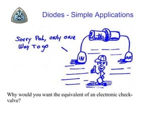
  • 1. Diodes - Simple Applications Why would you want the equivalent of an electronic check-valve?
  • 2. Diode Current-Voltage relationship The characteristics of all silicon based diodes are effectively the same, showing a sharp exponential increase in current at forward bias and only a few  As at reverse bias. Note that this “knee” is temperature-dependent as observed in lab 1. The non-ideal behavior shows a slower than exponential increase due to a series resistance, like the inductor. At large reverse-bias (not shown) current starts to flow. We will discuss this region later. 1N4148 characteristics
  • 3. Diode models A diode is often approximated as a 2-terminal device with ~0.7 v drop as long as 1-100 mA are flowing in the forward direction. The curves for a typical switching signal diode show why this is OK (note the log scale for current). When it is either reverse or weakly forward biased it is modeled as an open circuit. Real diodes and the symbol are shown. The arrow points in the direction of forward current flow.
  • 4. More Diode Physics Pure semiconducting materials like Silicon have very high resistivity at room temperature. However it can be made conductive by adding extra electrons. In n-type material this is done via atoms with one more electron than silicon (phosphorus). It can also be more conductive if one electron is removed, allowing the resulting “holes” to move about (they are really absences of valence or bonding electrons that hop from one site to the next). This is done in p-type material by adding elements with one less electron (aluminum). This is known as doping. An interesting thing happens if p- and n-type material are in contact. A region that has no holes on the p-side and no electrons on the n-side forms, called the depletion region. This area is like the original pure semiconductor and does not conduct, making the junction a very poor conductor again. However if it is biased (meaning a voltage is applied) with the p-type positive relative to the n-type, the depletion region shrinks. This is the origin of the one-way flow. The next slides describe why this is, using images from the website http://jas.eng.buffalo.edu/
  • 5. Diode Current-Voltage relationship (1) When material with lots of electrons (n-type) is brought into contact with material with lots of holes (p-type) the electrons and holes diffuse, resulting in a large current. However the loss of these carriers leaves a depleted region that is charged (because of the P and Al ions left behind) and reduces the current since the electric field repels the carriers.
  • 6. Diode Current-Voltage relationship (2) At zero bias electrons (holes) flow left (right) because of diffusion and an equal amount flow right (left) due to the electric field, resulting in no current. As the depletion region increases with reverse bias (not shown), the diffusion current to the left decreases leaving only a small reverse saturation current due to the field. Notice that for these doping levels the depletion region is 0.15 microns thick.
  • 7. Diode Current-Voltage relationship (3) At positive bias the depletion region is reduced and many electrons (holes) diffuse left (right) while only a small amount flow right (left) due to the electric field, resulting in a large current (sum of holes and electrons) flowing right. When an electron gets to the p-type material it recombines with a hole. If it does this in the depleted region the ideality factor N is 2, while it is 1 if recombination occurs outside. The depletion region is now only 0.05 microns thick.
  • 8. Types of diodes Power diodes (or rectifiers) - designed to handle large currents, typically used on power supplies or for switches. Typical values (for 1N4002) Max Average current: 1 A Peak current: 30 A Reverse voltage: 100 v Signal diodes - low powered, often faster switching (smaller depletion region). Typical values (for 1N4148) Max Average current: 100 mA Peak current: 450 mA Reverse voltage: 75 v Recovery time: 4 ns Zener diodes - voltage regulation, similar to power diodes but has any important specification: the zener voltage, V z (more later). Designed to breakdown at precise voltage (range 1-400 v).
  • 9. Clamp (or clipper) What does this circuit do? As mentioned in the text it “clamps” or “clips” the output voltage. If the magnitude of the input exceeds V batt +0.7 v, either negative or positive, the diode starts conducting. This limits the maximum voltage (this is similar to surge protectors). V bat One limitation of this is that by design it will distort a time-varying voltage input, cutting it off at a max and a min value. V in R V out
  • 10. Stiff Clamp V in C V out This circuit on the other hand works very well at higher frequencies in limiting the minimum voltage on the output. Treating the diode like a simple one-way switch we see that the output can never fall below -0.7 v, because then the diode begins conducting. How does the circuit do this? If the input voltage is less than this minimum, current flows counterclockwise, charging the left capacitor plate negative and the right plate positive. This capacitor voltage adds to the input, raising it to a minimum of -0.7 v, when current stops flowing. Note that it is the opposite if the diode is reversed because the currents flow clockwise.
  • 11. Zener diode - IV characteristics All diodes show a breakdown under reverse bias when the internal electric field gets very high, ripping electrons from atoms. This avalanche breakdown occurs typically at -50 to -1000 v. If the depleted region that acts like a barrier to current is thin there is another possibility. The electrons can quantum mechanically tunnel from the n- to the p-side, resulting in a reverse current. This can be engineered to occur at a precise voltage called the Zener voltage, V Z . V I V Z I II III The graph shows three distinct regions, as labeled. Region III is where zener diodes normally operate.
  • 12. Zener diode - voltage regulator (1) How can a zener regulator act to control the output voltage? In the circuit shown (note that the zener is connected so that it is reverse biased ) current flows through the zener and it is in region III, so the voltage drop across it is V Z . A zener only works as a regulator because it ensures that enough current is drawn through the series resistor so that the voltage drop results in V out =V Z . If no current flows through the zener (actually less than a few mAs) it no longer regulates because it is in region II. V out Unregulated V in
  • 13. Zener diode - voltage regulator (2) The voltage across the load is V Z since there is current through the zener (Region III) R R The voltage on the load is R load /(R+R load )V in because there is no current through the zener. R load Unregulated V in R load Unregulated V in